Note: Descriptions are shown in the official language in which they were submitted.
CA 02432069 2003-06-16
WO 02/052341 PCT/USO1/15268
MICROSTRUCTURED REAR PROJECTION SCREEN
The present invention is directed generally to a rear projection screen and
more
particularly to a rear projection screen that incorporates microstructures to
waveguide the
light passing through the screen and a light absorptive layer to enhance
contrast.
Background
Rear projection screens axe generally designed to transmit an image projected
onto
IO the rear of the screen into a viewing space. The viewing space of the
projection system
may be relatively large (e.g., rear projection televisions), or relatively
small (e.g., rear
projection data monitors). The performance of a rear projection screen can be
described in
terms of various characteristics of the screen. Typical screen characteristics
used to
describe a screen's performance include gain, viewing angle, resolution,
contrast, the
15 presence of undesirable artifacts such as color and speckle, and the like.-
It is generally
desirable to have a rear projection screen that has high resolution, high
contrast and a large
gain. It may also be desirable that the screen spread the light over a large
viewing space.
Unfortunately, as one screen characteristic is improved, one or more other
screen
characteristics often degrade. For example, the horizontal viewing angle may
be changed
20 in order to accommodate viewers positioned at a wide range of positions
relative to the
screen. However, increasing the horizontal viewing angle may also result in
increasing the
vertical viewing angle beyond what is necessary for the particular
application, and so the
overall screen gain is reduced. As a result, certain tradeoffs are made in
screen
characteristics and performance in order to produce a screen that has overall
acceptable
25 performance for the particular rear projection display application.
Summary of the Invention
Some rear projection screens include microstructures to waveguide light
passing
through the screen toward a viewer, with the space between the waveguides
filled with a
30 light absorptive material to enhance contrast. In such a construction,
however, some of the
light to be internally reflected in the waveguides can be lost due to
absorption in the light
absorptive material. One reason for this can be that the angle of incidence of
light in the
CA 02432069 2003-06-16
WO 02/052341 PCT/USO1/15268
waveguide is less than the critical angle necessary for total internal
reflection in the
waveguide given the index of refraction difference between the waveguide
material and
the light absorptive material.
In the present invention, a rear projection screen is provided that
incorporates
tapered waveguides and a light absorptive layer between the waveguides at the
front of the
screen that creates interstitial spaces between the waveguides that can be
comprised of air
or another low index medium. This allows for a larger index of refraction
difference at the
waveguide/interstitial region interface than when the entire interstitial
region is filled with
absorptive material. A larger index of refraction difference can be used to
increase screen
1 o efficiency as well as allow for screen designs that further enhance
contrast, provide for
larger viewing angles, and the like.
In one aspect, the present invention provides a rear projection screen that
includes a
plurality of waveguides disposed on a transmissive substrate, the waveguides
tapered from
a wider back portion near the substrate to a narrower front portion away from
the substrate,
15 and a light absorptive layer disposed between adjacent waveguides and
located at or near
the front portions of the waveguides, thereby defining interstitial regions
between adj acent
waveguides and the light absorptive layer, the interstitial regions having a
lower refractive
index than the waveguides.
In another aspect, the present invention provides a method for malting a rear
2o projection screen that includes disposing a plurality of waveguides on a
transmissive
substrate, the waveguides being tapered from a wider back portion near the
substrate to a
narrower front portion away from the substrate, and disposing a light
absorptive layer
between adj acent waveguides at or near the front portions of the waveguides,
thereby
defining interstitial regions between adjacent waveguides and the light
absorptive layer,
25 the interstitial regions having a lower refractive index than the
waveguides.
Brief Description of the Drawing
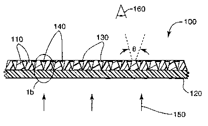
FIG. 1(a) is a schematic partial cross-section of a rear projection screen
according
to the present invention;
3o FIG. 1(b) is an enlarged view of area 1b from FIG. 1(a).
2
CA 02432069 2003-06-16
WO 02/052341 PCT/USO1/15268
FIGS. 2(a)-(c) are schematic partial perspective views of rear projection
screens
according to the present invention;
FIG. 3 is a schematic partial cross-section of a rear projection screen
according to
the present invention;
FIG. 4 is a schematic partial cross-section of a rear projection screen
according to
the present invention;
FIG. 5 is a schematic partial cross-section of a rear projection screen
according to
the present invention; and
FIG. 6 is a schematic partial cross-section of a rear projection screen
according to
to the present invention.
Detailed Description
FIG. 1(a) shows a projection screen 100 that includes a series of waveguides
110
disposed on a substrate 120. Alternatively, waveguides 110 and substrate 120
can be
integral. Waveguides 110 are tapered from a back side adjacent to the
substrate to a front
side oriented toward a viewer position 160. The degree of taper can be
measured by the
included angle between adjacent waveguides, designated 0 in FIG. 1(a). While
waveguides 110 are illustratively shown to have symmetric cross sections,
their cross
sections can also be asyrmnetric, for example having one side wall steeper
than another
side wall. In addition, although the tapered walls of the waveguides 110 are
shown in FIG.
1 (a) to be straight, they can also be curved, for example concavely or
convexly.
A light absorptive layer 130 resides between adjacent waveguides on the front
portions of the waveguides. Light absorptive layer 130 increases the contrast
of the screen
100 and reduces glare from ambient light present on the viewer side (viewer
position
represented by 160). Interstitial regions 140 exist between adjacent
waveguides and
absorptive layer. In operation, the projection screen 100 can be oriented so
that light 150
from a projector or other suitable display can be transmitted through the
screen 100 toward
a viewer position 160. Light may pass directly through a waveguide toward the
viewer or
may be reflected off a waveguide side wall and then directed through the
waveguide
toward the viewer.
3
CA 02432069 2003-06-16
WO 02/052341 PCT/USO1/15268
In some exemplary embodiments, the projection screen can include a rigid
substrate (not shown) on either the front side or back side (or both) of the
screen to give
structural integrity to the construction, for example.
In the present invention, the light absorptive layer is a layer that resides
at or near
the front portions of the waveguides, thereby creating the interstitial
regions. The
interstitial regions need not be filled with any particular material, and
indeed can be made
up of air or other such gaseous medium that has a refractive index that is 1
or nearly 1 (1
being the refractive index of vacuum). Alternatively, the interstitial regions
can be filled
with a non-gaseous material, preferably a low refractive index material. By
having an
to interstitial refractive index that is relatively low, preferably nearly
that of a vacuum, the
index difference between the waveguides and the interstitial regions can be
relatively
large, depending on the material of the waveguides.
For light incident on waveguide side walls at angles that exceed the critical
angle,
the light is totally internally reflected, thereby directed out of the
waveguide and toward
the viewer position. The greater the ratio of the index of refraction of the
waveguides 110
(index denoted nW) to the index of refraction of the interstitial regions 140
(index denoted
n;), the smaller the critical angle, and the more likely light will be totally
internally
reflected and directed with minimal losses toward the viewer. This can
increase the
throughput, and thus the efficiency, of the screen. For simplicity, and
without loss of
generality, the index of refraction ratio (nW/n;) encountered at the interface
between the
waveguide side walls and the medium of the interstitial regions will be
designated N in
this document. Using this terminology, it can be said that a larger N can lead
to a more
efficient screen because light is more likely to be totally internally
reflected, even over a
wider range of incident angles, without significant losses due to penetration
into the
interstitial regions.
A larger N can also allow screen designs that have a higher proportional
surface
area coverage of light absorptive material presented to the viewer, and
therefore higher
contrast. This concept can be understood by referring to FIG. 1 (b), which
shows an
enlarged view of region 1 b from FIG. 1 (a). FIG. 1 (b) shows a light ray R
that is incident
on a wall of a tapered waveguide at an angle al (measured from the normal to
the wall at
the point of incidence). Light ray R is reflected and encounters another
waveguide wall
4
CA 02432069 2003-06-16
WO 02/052341 PCT/USO1/15268
before leaving the waveguide. Because the waveguides are tapered, that is they
are wider
near their bases and narrower near their tops, the angle of incidence cc2 of
light ray R on
the second waveguide wall is smaller than al. If N is large enough, both al
and oc2 can
exceed the critical angle, and total internal reflection (TIR) can occur for
both reflections.
However, in cases where N is smaller, al may exceed the critical angle whereas
oc2 might
be smaller than the critical angle. In these cases, some light will be lost
due to the lack of
TIR unless the waveguides are made shorter so that light rays lilce light ray
R can exit the
waveguides before encountering a second side wall.
While shortening waveguides can lessen losses due to non-TIR reflections in
the
l0 waveguides due to multiple bounces in the waveguides, it also decreases the
proportional
area of the light absorptive material to the waveguide tops at the front of
the screen.
Referring to FIG. 1(b), the portion of layer 130 shown spans the gap between
the adjacent
waveguides 110 near the tops of the waveguides. If the waveguides were
truncated, the
gap between adjacent waveguides would be smaller, thus reducing the areal
coverage of
the light absorptive layer, thus reducing contrast. By providing for a larger
N, projection
screens of the present invention allow for the design of taller waveguides
(for a particular
taper angle) because the critical angle for TIR is smaller, thereby
accommodating more
multiple reflection situations such as shown in FIG. 1 (b). This in turn can
increase the
proportional area coverage of the light absorptive layer on the front of the
screen, which
increases contrast.
In addition to increasing efficiency and allowing for multiple TIR bounces in
the
waveguides, a larger N between the waveguides and the interstitial regions can
allow for
larger included wall angles (e.g., 0 in FIG. 1) while maintaining high
throughput. Larger
wall angles can lead to more space between adj acent waveguides at their tops,
which can
result in a higher proportional area of the absorbing layer and thus a higher
contrast.
Without such large index of refraction differences at waveguide walls,
increased wall
angles would result in a higher probability that light would not be totally
internally
reflected (larger wall angles reduces the angle of incidence for a given light
ray, as
measured from the normal to the incident surface). Such an effect is
counteracted by
3o increasing N, thereby reducing the critical angle and allowing for larger
wall angles while
CA 02432069 2003-06-16
WO 02/052341 PCT/USO1/15268
maintaining TIR. Higher wall angles can allow larger viewing angle ranges when
increasing the range of viewable angles in one or more dimensions is a
desirable property.
Projection screens of the present invention that have a relatively large N can
also
provide a larger range of viewing angles without substantial loss of light
intensity at higher
viewing angles. As described above, larger N means a lower critical angle,
which allows a
larger angular range of light to experience TIR in the waveguides and pass
through toward
the viewer without substantial losses in intensity. As a result, a larger
angular range of
light can exit the projection screen with relative uniformity in intensity
over a larger range
of viewing angles.
l0 Waveguides 110 can be any suitable material that is substantially
transmissive of
light within a desired range of wavelengths, and that can be molded or
otherwise formed
into appropriate shapes. For example, the waveguides can be made from
acrylates,
polycarbonates, epoxies, and other suitable materials. To obtain a large
refractive index
ratio between the waveguides and the interstitial regions, the waveguides
preferably have a
relatively high index of refraction, for example about 1.3 or higher, more
preferably about
1.4 or higher.
Waveguides can be provided on a substrate by impression molding, casting and
curing a material using a mold, selective polymerization of a curable
material,, or by
forming a film and selectively removing portions of the film to leave the
waveguide
structures. Preferably the bases, or back portions, of the waveguides are
closely packed to
fully or substantially cover the surface of the substrate on which they are
formed. In this
way, most of the light projected onto the back of the screen can be
transmitted through the
waveguides toward the viewer.
The waveguides can have any tapered shapes and dimensions suitable for a
particular application. Typically, the waveguides have heights of about 50
microns to
about 250 microns, maximum widths of about 50 microns to about X00 microns,
and
minimum widths of about 10 microns to about 400 microns. The side walls of the
waveguides are tapered and can be flat or curved. If the waveguides are
curved, they can
be curved concavely or convexly. Curved waveguides include those that are
piecewise
linear.
CA 02432069 2003-06-16
WO 02/052341 PCT/USO1/15268
While the waveguides are preferably substantially transmissive of visible
light (or
other desired portion of the spectrum), the waveguides can also include
appropriate
amounts of a colorant, such as a pigment or a dye, to provide filtering and/or
additional
contrast to the screen. Additionally, the waveguides can include particles,
voids, phase
dispersed materials, or other such elements to scatter and/or diffuse light as
it passes
through the waveguides. Such "scattering sites" can be symmetric or
asymmetric, and if
they are asymmetric they can be oriented, for example to scatter light
preferentially along a
desired axis. Suitable waveguides, materials, constructions, and methods of
making are
also described in commonly assigned U.S. Patent Application 09/348,809, which
to disclosure is incorporated into this document as if reproduced in full.
FIG. 2 illustrates some examples of waveguide shapes that can be used. As with
FIG. 1, the waveguides shown in FIG. 2 are symmetric for illustration, but
asymmetric
waveguide shapes can also be used. FIG. 2(a) shows a rear projection screen
200 that
includes rib-like waveguides 202 disposed on substrate 204. Light absorptive
layer 206
resides near the front of waveguides 202 and between the waveguides to create
interstitial
regions 208. By using rib-like waveguides, asymmetric viewing angles can be
achieved.
By varying the wall angles of the waveguides, the amount of viewing asymmetry
can be
altered.
FIG. 2(b) shows a rear projection screen 220 that includes post-like
waveguides
222 disposed on substrate 224. Waveguides 222 are shown to have square bases,
although
any suitably shaped base can be used. Light absorptive layer 226 resides near
the front of
waveguides 222 to create interstitial regions 228. By using square, post-like
waveguides,
the viewing angle can be made symmetric. In addition, post-lilce waveguides
provide
another degree of freedom when making asymmetric waveguides. For example, the
angle
between adjacent post-like waveguides in the vertical screen direction can be
made
different from the angle between adjacent post-like waveguides in the
horizontal direction.
This can provide for a different range of vertical and horizontal viewing
angles, for
example. This is one degree of freedom for design asymmetry. The other degree
of
freedom is in designing post-like waveguides that have a steep wall taper on
one side and a
3o shallow wall taper on the opposing side, for example. This can provide a
difference in
viewing angle from left to right and/or from up to down. The terms horizontal,
vertical,
CA 02432069 2003-06-16
WO 02/052341 PCT/USO1/15268
left, right, up, and down are used illustratively, and with particular regard
to FIG. 2(b), and
should not be read to limit the scope of the present invention. In addition to
providing
more design freedom, using post-like waveguides can provide for a large
proportion of the
front area of screen 220 being covered by the light absorptive layer 226, as
can be seen in
FIG. 2(b). This can result in high contrast and glare reduction.
FIG. 2(c) shows a rear projection screen 240 that includes cone-like
waveguides
242 disposed on substrate 244. Unlike in FIG. 2(b), waveguides 222 are shown
to have
circular bases. Light absorptive layer 246 resides near the front of
waveguides 242 to
create interstitial regions 248. Again, a large proportion of the front area
of screen 240 is
l0 covered by the light absorptive layer 246, resulting in high contrast and
glare reduction.
Throughput can be increased when using post-like waveguides by employing a
close-packed arrangement of posts, for example a hexagonal arrangement.
Referring back to FIG. 1, substrate 120 can be any suitable material that is
substantially transmissive of a desired range of wavelengths and that
optionally can
provide desired mechanical integrity to the screen. Examples of suitable
materials
includes polycarbonates, glass, polyethylene terapthalate (PET), and other
suitable
substrate materials. Substrate 120 can be the same material used for
waveguides 110, and
can be formed simultaneously with the waveguides so that the waveguides and
the
substrate are integral. Alternatively, the waveguides can be bonded to the
substrate during
2o molding of the waveguides or by using a laminating adhesive (e.g., an
optically clear
adhesive). Additionally, the waveguides can be formed on the substrate by a
cast and cure
method. Preferably substrate 120 has an index of refraction that is about the
same as the
index of refraction of the waveguides 110.
It may be desirable to give the back surface of the substrate, that is the
surface of
the substrate oriented away from the waveguides, a matte surface to reduce
glare from the
image light source. Depending on the particular construction used, when the
baclc of the
substrate is not a matte surface, some light from the imager can be specularly
reflected off
the back of the substrate and be redirected baclc through the screen at a
different position
than what was intended. This can cause ghost image formation.
3o Absoytive layer 130 typically includes a mixture of a light absorptive
material
dispersed in a binder. Suitable light absorptive materials include carbon
black, light
CA 02432069 2003-06-16
WO 02/052341 PCT/USO1/15268
absorptive dyes such as black dyes or other dark dyes, light absorptive
pigments or other
dark pigments, and other suitable materials. Suitable binders include
thermoplastics,
radiation cured or thermoset acrylates, epoxies, silicone-based materials, or
other suitable
binder materials. Other materials such as dispersants, surfactants, viscosity
modifiers,
curing agents, and the like can also be included. In preferred configurations,
the
proportion of the waveguide wall area that is contacted by the light
absorptive layer is
relatively small. As such, there is less of a concern as to the relative
refractive indices of
the light absorptive layer and the waveguides. When absorptive layer 130 is
the outermost
layer of the projection screen 100, it may be desirable to provide the outer
surface (the
to surface oriented toward the viewer) with a matte texture. This can reduce
glare, especially
due to glancing reflections from ambient light. In some cases, the light
absorptive layer
130 is not the outermost layer of the projection screen 100. For example, a
polarizes such
as a linear polarizes or circular polaxizer, a matte substrate, other
desirable film,
component, or device can be provided as the outermost layer. Such other
elements can
provide desirable optical, aesthetic, mechanical, and/or chemical properties
as well as
added functionality (for example, a touch panel user interface).
Absorptive layer 130 can be disposed over waveguides 110 in a variety of ways.
For example, the light absorptive layer can be extruded directly onto the
waveguide tops.
Extrusion of a suitable absorptive layer material onto the waveguides can be
accomplished
so that the light absorptive layer material remains near the front of the
waveguides and
does not fill the interstitial regions. The ability to extrude absorptive
layer material
without filling the interstitial regions between the waveguides depends on the
dimensions
of the waveguides (particularly the distance between waveguides at the front
portions of
the waveguides), the thickness of the light absorptive layer being extruded,
the viscosity of
the light absorptive layer during extrusion, and/or the temperature of the
waveguide
substrate. Preferably, when the extrusion method is used, a thermoplastic
absorptive layer
material is extruded over the waveguides, the thermoplastic absorptive layer
material
cooling sufficiently quickly upon contact with the waveguides that the light
absorptive
layer material does not flow or seep down into the interstitial valleys.
3o In some cases when the light absorptive layer is extruded over the
waveguides, a
residual amount of the light absorptive layer might remain on the tops of the
waveguides
CA 02432069 2003-06-16
WO 02/052341 PCT/USO1/15268
where light exits toward the viewer. In some cases, this can undesirably
reduce the
intensity of light directed toward the viewer due to absorption of light in
the residual
absorptive layer. It may be desirable then to co-extrude a clear layer and a
light absorptive
layer over the waveguides, the clear layer oriented toward the viewer
position. The result
may be as shown in FIG. 3 where rear projection screen 300 includes a
plurality of
waveguides 310 disposed on a substrate 320, with co-extruded bilayer 330
disposed on the
front portions of the waveguides 300. Bilayer 330 includes a light absorptive
layer 332
and a clear layer 334. As shown, a portion of the bilayer 330 covers the tops
of the
waveguides. Because the upper layer of the bilayer is clear, the bilayer can
be extruded
to over the waveguides so that the portion of the bilayer covering the tops of
the waveguides
is a portion of the clear layer rather than the light absorptive layer. The
bilayer is
preferably thin enough so that interstitial regions 340 are created between
adjacent
waveguides 310 and the light absorptive layer 332. Also, the clear layer 334
preferably
has about the same index of refraction as the waveguides to reduce intensity
losses due to
interface reflections.
While the term clear layer is used, it is understood that any suitable
material that is
substantially transmissive of light in a desired range of wavelengths can be
used. It is also
contemplated that the clear layer can contain material to increase contrast
and/or to diffuse
or scatter light as it exits the waveguides. Additionally, when the clear
layer is the
outermost layer of the screen, the clear layer can be imparted with a matte
outer surface to
reduce glare, for example due to ambient light reflections.
Extruding the light absorptive layer over the waveguides can also be used to
alter
the shape of the front portions of the waveguides. For example, when the
waveguides are
made of a thermoplastic material that softens at temperatures used to extrude
the light
absorptive layer, contact of the extruded absorptive layer with the waveguides
can cause
the tops of the waveguides to "mushroom". This can be seen in FIG. 4, which
shows a
rear projection screen 400 that includes a series of waveguides 410 disposed
on a substrate
420. Absorptive layer 430 has been extruded over the thermoplastic waveguides
410, and
as a result the tops of waveguides 410 have softened to form lenslets 412. The
formation
3o of lenslets 412 can be used to change the angular dispersion of light in
one or more
directions as it exits the waveguides toward the viewer. While the extruded
absorptive
CA 02432069 2003-06-16
WO 02/052341 PCT/USO1/15268
layer is hot enough to soften the waveguides, the light absorptive layer
preferably cools
rapidly enough to maintain an interstitial region 440 between adjacent
waveguides 410 and
the light absorptive layer 430.
FIG. 5 shows an analogous situation to FIG. 4 where the extruded "layer" is a
bilayer 530 of a light absorptive material 532 and a clear material 534. The
screen 500
includes waveguides 510 disposed on a substrate 520. Waveguide 510 have
lenslets 512
formed on their front portions during extrusion of the bilayer 530. Bilayer
530 can be
extruded so that the pouion of the bilayer 530 remaining between lenslets S 12
and the
viewer is the clear layer 534. Preferably, interstitial regions 540 are
created between
adjacent waveguides 510 and absorptive layer 532.
Lenslets on the front portions of tapered waveguides on projection screens can
be
formed by methods other than extrusion of a light absorptive layer onto
thermoplastic
waveguides. For example, a screen that includes a series of tapered
thermoplastic
waveguides disposed on a substrate can be provided. Next, a light absorptive
material can
be filled into the spaces between the waveguides. Then, the top portions of
the
waveguides can be reshaped by passing the assembly through a nip roll,
optionally a
heated nip roll, that "mushrooms" the tops of the waveguides, thereby forming
lenslets.
Variations of this method of forming lenslets, the extrusion methods discussed
above, and
other suitable methods of forming lenslets or of re-shaping tapered waveguides
are
contemplated in the present invention.
Absorptive layers can be formed over waveguides on projection screens of the
present invention by methods other than extrusion. For example, a light
absorptive layer
can be laminated over, or otherwise pressed onto, the waveguides. To
illustrate, FIG. 6
shows a projection screen 600 that includes a series of tapered waveguides 610
disposed
on a substrate 620. A light absorptive layer 632 can be coated or otherwise
disposed on a
carrier layer 634 to form a "lamination assembly" 630. Lamination assembly 630
can then
be laminated (or pressed) over the waveguides 610 with the light absorptive
layer 632
contacting the waveguide tops. Preferably the light absorptive layer is at
least somewhat
flowable during lamination so that absorptive layer material between the
waveguide tops
3o and the carrier layer can be pushed out to surrounding areas. For example,
the light
absorptive layer can include a hot melt adhesive composition that can flow
somewhat with
11
CA 02432069 2003-06-16
WO 02/052341 PCT/USO1/15268
the application of pressure and/or heat. As another example, the light
absorptive layer can
include a radiation curable material that can be pressed onto the waveguides
before curing
and then hardened on the waveguides by exposure to suitable radiation, such as
ultraviolet
light.
The viscosity of the light absorbing material during lamination can affect the
ability to laminate the light absorptive layer on the waveguides in a
desirable manner. If
the viscosity is too low, the light absorptive layer material might
undesirably flow down
into the grooves between the waveguides. If the viscosity is too high, it may
be difficult
too press the light absorptive layer material out of the spaces at the tops of
the waveguides.
to Preferably, the light absorptive material has a viscosity of about 50,000
cps to about
200,000 cps at the laminating temperature. In exemplary cases when the light
absorptive
layer is to be laminated over the waveguides, the light absorptive layer
material has a
viscosity that is about 100,000 cps at the laminating temperature.
Optionally, an adhesive can be used between the waveguide tops and the light
15 absorptive layer to promote adhesion. Carrier layer 634 can be removable or
can remain
with the screen. When the carrier layer remains as part of the screen, it is
preferred that the
carrier layer is substantially transmissive of light within a desired range of
wavelengths,
and that the index of refraction of the carrier layer is about the same as the
refractive index
of the waveguides. Optionally, the carrier layer can include materials for
contrast
2o enhancement, light diffusion or scattering, etc. When the carrier layer
remains as the
outermost layer of the screen, it may be imparted with a matte surface to
reduce glare. As
noted above, other elements such as linear or circular polarizers, rigid
substrates, touch
panels, and any other suitable element that can provide desired properties
and/or
functionalities can also be added.
12
CA 02432069 2003-06-16
WO 02/052341 PCT/USO1/15268
Examples
Objects and advantages of this invention are further illustrated by the
following
examples, but the particular materials and amounts thereof recited in these
examples, as well
as other conditions and details, should not be construed to unduly limit this
invention.
Example 1
A rear proj ection screen was made in the following manner.
Rib-like waveguides like those shown in FIG. 2(a) and having cross-sections
such
as depicted in FIG. 1 (a) were made according to the following procedure. A
resin
1o formulation was made from 80% by weight of a urethane acrylate oligomer and
20% by
weight of 2-phenoxyethyl acrylate. The refractive index of the resin was
approximately
1.51. Particles were then mixed into the resin formulation. The particles were
a
copolymer blend of ethyl methacrylate and polystyrene, and had an index of
refraction of
approximately 1.54. The average particle diameter was about 5 microns with a
standard
15 deviation of about 0.5 microns. A particle loading of 15% by weight
relative to the resin
was used. The particles were well dispersed using a high shear blender. A
photoinitiator
was added into the mixture in an amount of 2% by weight of the resin.
The mixture was then cast on a metal mold that had indentions with dimensions
corresponding to the desired rib waveguide dimensions. An approximately 0.25
mm thick
2o polycarbonate film (commercially available from Bayer Corporation) was
applied on top
of the resin in the mold and pressed in place using a roller. Excess resin was
removed so
that the pattern in the mold was filled with no excess that would form a land.
The resin
was then cured in place and adhered to the polycarbonate substrate. The
substrate and the
cured matrix were then removed from the tool leaving a clean metal mold for
reuse. The
25 resulting rib-like waveguides were about 250 microns tall as measured from
the substrate,
about 162 microns wide at their base, had an included wall angle of 18.5
°, and had
symmetric cross-sections. The rib tops were about 81 microns wide, thereby
giving a
proportional coverage of absorptive material at the front of the screen upon
application of
the light absorptive layer of about 0.5 of the total area of the screen.
30 A light absorptive material was then extruded over the rib-like waveguides.
The
binder for the extrudable light absorptive material was an acid/acrylate-
modified ethylene
13
CA 02432069 2003-06-16
WO 02/052341 PCT/USO1/15268
vinyl acetate polymer commercially available from DuPont under the trade
designation
Bynel 3101. For extruding, a three-quarter inch general purpose single screw
Killion
extruder with a gear pump and a six inch die was used. There were a total of
four zones in
the extruder, which were held at temperatures of 170°C, 179°C,
190°C and 198°C,
respectively. The die temperature was held at 219°C.
Polyethylene/carbon black
concentrate pellets were added to the binder at to achieve about a 1 % by
weight
concentration of carbon black pellets to the binder. The black pellets were
mixed with the
binder pellets in the single screw of the extruder to produce an extrudable
light absorptive
material. Constant throughput was maintained by the gear pump set to 7.0 rpm
in order to
to produce an approximately 50 micron thick film at about 2.3 centimeters per
second (about
4.5 feet per minute). The gap was set to about 0.4 mm (or 15 mils). The light
absorptive
material was extruded onto the tops of the rib-like waveguides with the
direction of motion
being parallel to the ribs. Very little of the light absorptive material
remained on the tops
of the waveguides and the resulting screen was similar to that shown in FIG. 1
(a).
The resulting screen sample was measured to have a peals gain of 2.20, a
horizontal
viewing angle of 46.5° (horizontal viewing angle = angular viewing
range in a direction
perpendicular to the ribs measured at the half peals gain points), and a
vertical viewing
angle of 18° (vertical viewing angle = angular viewing range in a
direction parallel to the
ribs measured at the half peak gain points). Total transmission of the screen
was
approximately 72%.
Example 2
A rear projection screen was made in the following manner.
A series of parallel rib-like waveguides were formed on a polycarbonate
substrate
as in Example 1. The waveguides and substrate were the same materials and had
the same
dimensions as reported in Example 1.
Next, the following light absorptive coating formulation was weighed and
mixed:
10 grams of a urethane acrylate (commercially available from Sartomer, Exton,
PA, under
the trade designation CN963E75), 0.5 grams of carbon blacle dispersion
(commercially
available from Penn Color, Doylestown, PA.), 5 grams of methyl ethyl ketone
(MEK), and
0.2 grams of a photoinitator (commercially available from Giba Geigy,
Hawthorne, NY,
14
CA 02432069 2003-06-16
WO 02/052341 PCT/USO1/15268
under the trade designation Daracure 4265). The formulation was coated on to
an
approximately 0.13 mm thick polyester film. Coating of the formulation was
performed
using a wire-wrapped rod. The resulting coating had a wet thickness of about
55 microns.
After coating, the film was air dried to evaporate the MEK. The dry thickness
of the
coating was about 38 microns.
The dried light absorptive coating was then laminated at room temperature to
the
tops of the rib-like waveguides. Lamination was performed using a nip roll
with two
rubber rolls. The laminate construction was then exposed to ultraviolet
radiation using a
Fusion D lamp at a dose of about 0.7 Joules/cm2 to cure the light absorptive
coating. The
to resulting screen structure was similar to that shown in FIG. 6. The screen
sample was
measured to have a peak gain of 3.2, a horizontal viewing angle of 28°,
a vertical viewing
angle of 17°, and a total throughput of 68%.