Note: Descriptions are shown in the official language in which they were submitted.
CA 02433761 2003-07-04
WO 02/056509 PCT/JPO1/00027
DES C RIPTION
CONTROL SCHEME FOR LONG WAVELENGTH
CHANNELS IN WIDEBAND WDM OPTICAL FIBER
s TRANSMISSION SYSTEM
TECHNICAL FIELD
The present invention relates to wide-band WDM
(Wave Division Multiplexing) transmission systems and a
s o protection scheme for the long wavelength channels in such
systems against failure in the absence of the short wavelength
signals.
BACKGROUND ART
1 s The optical communication system of the related art
comprises a transmitting terminal for generating a WDM optical
signal formed by wavelength-division multiplexing of a plurality
of optical signals of different wavelengths, an optical
transmission line for transmitting the WDM optical signal
2 o transmitted from the transmitting terminal and a receiving
terminal fox receiving the transmitted WDM optical signal.
Moreover, this optical communication system comprises, as
required, one or a plurality of optical repeaters having the
function to amplify the WDM optical signal in the course of the
2 s optical transmission line.
In such an optical communication system, the
waveform of each optical signal is deteriorated due to non-linear
optical effects in the optical transmission line. In order to
eliminate the deterioration of the waveform, it is effective to
3 o reduce the optical power of the optical signals launched into the
transmission line, but a reduction of the optical power results in
an increase of the optical signal to noise ratio (OSNR) due to
noise accumulation in the optical amplifiers.
For this purpose, it has been proposed to use a
35 combination of discrete optical amplifiers provided within
repeaters and distributed optical amplifier using the optical
transmission line in common as the optical amplifying medium.
-1-
CA 02433761 2003-07-04
WO 02/056509 PCT/JPO1/00027
In a discrete optical amplifier the amplifying medium and pump
light source are centralized in one area. In contrast, the
amplifying medium of a distributed optical amplifier is laid
between two remote places and pump light source is provided in
one or both places.
Fiber doped optical amplifiers represent one group of
optical fiber amplifiers. In doped fiber amplifiers a lanthanide
rare-earth element is added to the optical fiber. The structure of
electronic excitation levels of lanthanide rare-earth atoms allows
1 o for amplification by stimulated emission in the low-absorption
wavelength domain of optical fibers. The operation bandwidth is
limited to certain wavelength ranges: Neodymium (Nd) amplifies
in the 1060nm wavelength band, Praseodymium (Pr) in the 1300
nm wavelength band, Thulium (Tm) in the 1450 nm wavelength
band and Erbium (Er) in the 1550 nm band.
The other group of optical fiber amplifier takes
advantage of stimulated Raman scattering (SRS) an inelastic
scattering process between photons and optical phonons of lattice
vibrations. It has a wide gain width and a gain shift of 13.3 THz
2 0 (about 100 nm), as will be described later with reference to Fig. 4.
In contrast to erbium doped fiber amplifiers, the SRS effect
occurs also in ordinary optical fibers. Moreover, the pumping
wavelength can be set for any amplification wavelength.
The low loss transmission window in silica-based
optical fibers covers the wavelength range from 1450-1650 nm
with a minimum around 1550 nm. Until recently, only Erbium
doped fiber amplifiers (EDFA) which cover the so-called C-band
(1530-1565 nm) and the gain-shifted EDFA which cover the so-
called L-band (1570-1605 nm) were employed. In these systems
3 o the pump wavelengths for distributed Raman amplification (DRA)
are much shorter than the signal wavelengths.
The increasing demand for transmission capacity of
optical fiber systems requires the expansion of the optical
bandwidth in a single fiber. Extension to longer wavelengths has
several drawbacks. The loss profile in this wavelength domain
varies strongly among installed fibers, which makes system
design more difficult and materials and technologies for optical
CA 02433761 2003-07-04
WO 02/056509 PCT/JPO1/00027
components (e.g. photodiodes) yet have to be developed. Raman
amplification is in principle available fox this wavelength domain.
However, the pump wavelengths would partly overlap with the
short wavelengths signals in the C-band.
On the short wavelength side below 1530nm, the low
loss region of silica-based fibers extends to 1450 nm. Raman
pump wavelengths for this region do not overlap with signals;
however, they are located at the water-peak of optical fibers,
where the absorption loss is high. Nevertheless, due to the
1 o availability of high-power pump lasers, Raman amplification is a
feasible technology for this wavelength domain. Besides,
Thulium doped amplifiers and gain-shifted Thulium doped
amplifiers are candidates as amplifiers for wavelength bands
below 1530 nm. The additional wavelength regions are referred
15 to as S+ band (1450-1490 nm) and S band (1490-1530 nm). In
these new wide-bandwidth systems, the short wavelength signals
act as DRA pump light with respect to the long wavelength
signals. S+ and S band wavelengths transfer optical power to the
C and L band channels via SRS. Distributed Raman pumping of
2 o the S+ and S band channels compensates the power depletion due
to SRS as well as the increased fiber loss at S+ and S wavelengths.
If all wavelengths are in service, the power transfer is balanced.
A further description will be given of the
conventional optical communication system with reference to the
2 5 accompanying drawings.
Fig. 1 is a graph of a typical optical loss spectrum of
silica-based optical fibers in which the low loss region covers the
wavelength range from 1450 to 1650 nm. Optical amplifiers
allow simultaneous amplification of a group of wavelengths. The
3 o C and L band correspond to the wavelength ranges of Erbium
doped and the gain-shifted Erbium doped amplifiers. The S+ and
S band are related to the wavelength ranges of Thulium doped and
gain-shifted Thulium doped fiber amplifiers. When light of 1450
nm and 1550 nm travels 100 km through an optical fiber with a
35 loss of 0.26 dB/km, it experiences a loss of 26 dB and 20dB,
respectively. Thus, light with a wavelength of 1450 nm
experiences a loss of about 0.06 dB/km higher than the lowest
-3-
CA 02433761 2003-07-04
WO 02/056509 PCT/JPO1/00027
loss wavelength.
Fig. 2A shows a conventional WDM transmission
system. Symbols of optical components in the accompanying
drawings including Fig. 2A are defined as shown in Figs. 3A
through 3F. Fig. 3A shows various types of optical amplifiers.
The C and L band can be amplified either separately by means of
a broadband C/L band amplifier. Accordingly, S and S+ bands
can be amplified either by separate doped fiber amplifiers or
Raman amplifiers, or by amplifiers covering the whole S+ and S
s o band wavelength range. For this group of amplifiers a double
lined triangle is used in this specification. Variable optical
attenuators (VOA) can be added to the amplifiers as means for
adjusting the amplifier output power.
Fig. 3B shows an optical circulator, and Fig. 3C
shows an optical tap. Fig. 3D shows an optical switch. Figs. 3E
and 3F show a WDM coupler.
Turning to Fig. 2A again, the WDM transmission
system includes a transmitter, a transmission fiber connecting
remote locations, discrete optical amplifier to compensate for the
2 o fiber loss, and a receiver. Multiple wavelengths transmission
enhances the transmission capacity. The optical amplifiers add
noise in the form of amplified spontaneous emission, which
reduces the optical signal-to-noise ratio, thus giving rise to errors
in the signal detection. Distributed Raman amplification can
2 5 improve the signal to noise ratio because it amplifies the signals
along the transmission fiber. Moreover, the stimulated Raman
scattering tilt, which will be described later in detail, can be
compensated for in the system. There are control schemes that
allow adjusting the spectral tilt under changing conditions of C
3o and L band channel usage (OECC'99, "Optical SNR degradation
due to stimulated Raman scattering in dual-band WDM
transmission systems and its compensation by optical level
management", T. Hoshida, T. Terahara, 3. Kumasako and H.
Onaka).
3 5 Distributed Raman amplification generally is not
high enough to make discrete amplifiers obsolete. As shown in
Fig. 2B, counter-propagating amplification is used to average out
-4-
CA 02433761 2003-07-04
WO 02/056509 PCT/JPO1/00027
bit-pattern dependent amplification causing power fluctuations.
Commercial systems employ C and L band amplifiers. In the
laboratory triple band (S, C, L) transmission has been
demonstrated (ECOC2000, "Experimental Study on SRS loss and
its compensation in three-band WDM transmission", Yutaka Yano,
Tadashi Kasamatsu, Yoshitaka Yokoyama and Takashi Ono), as
shown in Fig. 2C.
In dense WDM systems, channel-interleaved bi-
directional transmission as shown in Fig. 2D can reduce
Zo impairments due to nonlinear interaction between adjacent
channels (cross phase modulation, four wave mixing) and thus
allows increasing the spectral efficiency of the system. At the
amplifier stage, optical circulators (directional coupling elements)
separate forward and backward propagating channels.
Fig. 4 shows the optical power depletion due to
stimulated Raman scattering and fiber loss. In wide-band WDM
transmission systems with high channel count, SRS causes a
strong power transfer from the short wavelengths to long
wavelengths. The Raman gain depends on the frequency shift
2 o between the shorter and the longer wavelength. It has a maximum
around 13.3 THz in silica-based fibers. Thus, for distributed
Raman pumping it is most effective to allocate the pump
wavelength shifted about 100 nm to shorter wavelength with
respect to the signal wavelengths. In wide band WDM systems
2 5 the short wavelength signals become efficient pump light sources
for the long wavelength channels.
Fig. 5 shows SRS-spectral tilt compensation using
DRA and pre-emphasis (repeater output level control). Using pre-
emphasis and distributed Raman amplification of the short
3o wavelength channels, the higher absorption loss and the SRS
power depletion can be compensated (ECOC2000, "Experimental
Study on SRS loss and its compensation in three-band WDM
transmission", Yutaka Yano, Tadashi Kasamatsu, Yoshitaka
Yokoyama and Takashi Ono). It is to be noted that the power
3 5 transfer is balanced if all channels are on.
However, in wide-bandwidth systems, an interruption
of the operation of the short wavelength channels (either by
-5-
CA 02433761 2003-07-04
WO 02/056509 PCT/JPO1/00027
failure or for the purpose of maintenance) or a reduced number of
active short wavelength channels result in less or no power
transfer to the C and L band signals. As a consequence, the C and
L band signal output power drops and the OSNR degrades,
making these channels more error-prone.
Thus, a general object of the present invention is to
provide a control scheme for long wavelength channels in
wideband WDM optical fiber transmission system in which the
above problem is overcome.
s o A more specific object of the present invention is to
provide an optical amplifier device capable of protecting long
wavelength channels of wideband optical fiber transmission
systems in which the power transfer from the short to the long
signal wavelengths due to stimulated Raman scattering is
i5 essential for the transmission of the long wavelength signals.
Another object of the present invention is to provide
an optical communication system utilizing the above protection
scheme.
2 o DISCLOSURE OF THE INVENTION
The above objects of the present invention are
achieved by an optical amplifier device used for a system in
which a power transfer takes place from comparatively short
wavelength signal to a comparatively long wavelength signal, the
2 5 optical amplifier device comprising: an amplifier stage coupled to
an optical transmission medium; a monitor monitoring a status of
a first band; and a pump light source unit supplying at least one
first pump light to the optical transmission medium on the basis
of the status of the first band monitored, so that the above at least
one first pump light supplies additional power to longer
wavelength channels related to the status of the first band.
The above objects of the present invention are also
achieved by an optical amplifier device used fox a bi-directional
system in which a power transfer takes place from comparatively
35 short wavelength signal to a comparatively long wavelength
signal, the optical amplifier device comprising: first and second
amplifier systems; and directional coupling elements coupling the
-6-
CA 02433761 2003-07-04
WO 02/056509 PCT/JPO1/00027
first and second amplifier stages to an optical transmission
medium. Each of the first and second amplifier systems
comprises: an amplifier stage coupled to the optical transmission
medium; a monitor monitoring a status of a first band; and a pump
light source unit supplying at least one first pump light to the
optical transmission medium on the basis of the status of the first
band monitored, so that the above at least one first pump light
supplies additional power to longer wavelength channels related
to the status of the first band.
1 o The above objects of the present invention are also
achieved by a method of controlling an optical amplifier device,
comprising the steps of: monitoring a status of a first band; and
supplying at least one first pump light to an optical transmission
medium on the basis of the status of the first band monitored, so
that the first pump light supplies additional power to longer
wavelength channels related to the status of the first band.
The above objects of the present invention are also
achieved by an optical transmission system comprising: optical
amplifier devices; and an optical transmission medium coupling
2 o the optical amplifier devices. One of the optical amplifier devices
comprises: an amplifier stage coupled to the optical transmission
medium; a monitor monitoring a status of a first band; and a pump
light source unit supplying at least one first pump light to the
optical transmission medium on the basis of the status of the first
2 5 band monitored, so that the above at least one first pump light
supplies additional power to longer wavelength channels related
to the status of the first band.
The above objects of the present invention are
achieved by a bi-directional optical transmission system in which
3 o a power transfer takes place from comparatively short wavelength
signal to a comparatively long wavelength signal, the bi
directional optical transmission system comprising: optical
amplifier devices; and an optical transmission medium coupling
the optical amplifier devices. One of the optical amplifier devices
35 comprises: first and second amplifier systems; and directional
coupling elements coupling the first and second amplifier stages
to the optical transmission medium. Each of the first and second
CA 02433761 2003-07-04
WO 02/056509 PCT/JPO1/00027
amplifier systems comprises: an amplifier stage coupled to the
optical transmission medium; a monitor monitoring a status of a
first band; and a pump light source unit supplying at least one
first pump light to the optical transmission medium on the basis
of the status of the first band monitored, so that the above at least
one first pump light supplies additional power to longer
wavelength channels related to the status of the first band.
BRIEF DESCRIPTION OF THE DRAWINGS
s o Other objects, features and advantages of the present
invention will become more apparent from the following detailed
description when read in conjunction with the accompanying
drawings, in which:
Fig. 1 is a graph showing typical fiber Ioss in the
15 1450-1600 nm wavelength domain of silica-based single mode
fibers;
Figs. 2A through ZD are block diagrams of
conventional optical communication systems;
Figs. 3A through 3F are diagrams of symbol
2 o definitions of optical components;
Fig. 4 is a diagram showing optical power depletion
due to SRS and fiber loss;
Fig. 5 is a diagram showing SRS-spectral tilt
compensation using DRA and pre-emphasis;
2 5 Fig. 6 is a diagram showing the principle of the
present invention;
Fig. 7 is a block diagram of an optical transmission
system according to a first embodiment of the present invention;
Fig. 8 is a block diagram of an optical repeater node
3 o formed of an amplifier device used in the optical transmission
system shown in Fig. 7;
Fig. 9 is a block diagram of a Raman pump light
source unit shown in Fig. 8;
Figs. 10A and 10B are diagrams showing a control
3 5 operation of a CPU shown in Fig. 9;
Fig. 11 is a block diagram of an optical transmission
system according to a second embodiment of the present
_g_
CA 02433761 2003-07-04
WO 02/056509 PCT/JPO1/00027
invention;
Figs. 12A and 12B are diagrams showing a control
operation of a CPU shown in Fig. 11;
Fig. 13A is a block diagram of an optical repeater
node according to a third embodiment of the present invention;
Figs. 13B, 13C, and 13D are diagrams of variations
of the optical repeater node shown in Fig. 13A;
Fig. 14A is a block diagram of an optical repeater
node according to a fourth embodiment of the present invention;
z o Fig. 14B is a block diagram of a variation of the
repeater node shown in Fig. 14A;
Fig. 15A is a block diagram of an optical repeater
node according to a fifth embodiment of the present invention;
Fig. 15B is a block diagram of a variation of the
15 repeater node shown in Fig. 15A;
Fig. 16A is a block diagram of another val-iation of
the repeater node shown in Fig. 15A;
Fig. 16B is a block diagram of a variation of optical
repeater node;
2 o Fig. 17A is a block diagram of an optical repeater
node according to a sixth embodiment of the present invention;
Fig. 17B is a block diagram of a variation of the
repeater node shown in Fig. 17A;
Fig. 18A is a block diagram of an optical repeater
node according to a seventh embodiment of the present invention;
Fig. 18B is a block diagram of a variation of the
repeater node shown in Fig. 18A;
Fig. 19A is a block diagram of an optical repeater
node according to an eighth embodiment of the present invention;
3 o Fig. 19B is a block diagram of a variation of the
repeater node shown in Fig. 19A;
Fig. 20A is a block diagram of an optical repeater
node according to a ninth embodiment of the present invention;
Fig. 20B is a block diagram of a variation of the
35 repeater node shown in Fig. 20A;
Fig. 2I is a block diagram of an optical repeater node
according to a tenth embodiment of the present invention;
_g_
CA 02433761 2003-07-04
WO 02/056509 PCT/JPO1/00027
Fig. 22 is a block diagram of an optical repeater node
according to an eleventh embodiment of the present invention;
Fig. 23 is a block diagram of an optical repeater node
according to a twelfth embodiment of the present invention;
Fig. 24 is a block diagram of a variation of the
repeater nodes shown in Figs. 20A, 20B and 21 through 23; and
Figs. 25A and 25B are block diagrams of optical
setups fox monitoring part of the forward and the backward
propagating lights by using optical spectrum analyzers.
BEST MODE FOR CARRYING OUT THE INVENTION
A description will first be given of the principle of
the present invention.
According to one aspect of the present invention,
additional Raman pump light sources are provided in the
amplifier stages. These sources are off when the S+ and the S
band are in full service. Photodiodes monitor the power levels of
the S+ and S bands. Depending on the position of the
photodiodes the control signal is used to switch on/off the
2 o substitute Raman pump laser diodes in the same repeater node or
in the previous or next one node. The photodiodes can either be
located before or behind the amplifier. Thus, it is possible to
maintain a reliable C/L band transmission also without full
operation of the S+ and S band channels.
2 5 Referring to Fig. 6, in the case of the absence of all
S+ and/or S band channels or parts of the channels, the power
transfer from the shorter to the longer wavelengths is reduced or
completely interrupted. As a consequence, the power of C and L
band channels drops and the OSNR suffers, leading to a higher
3 o error probability for these channels. Therefore, a back-up system
and a control mechanism are required, which provide optical
pump power to the C and L band channels in the case of the
absence of the S+ and/or S band or parts of these bands. In
addition, an increase of the C and L band repeater output power of
3 5 each amplifier stage can improve the system performance in the
absence of the short wavelength bands or parts of these bands.
More particularly, if the S+ band is totally or partly
-10-
CA 02433761 2003-07-04
WO 02/056509 PCT/JPO1/00027
off or the power level of the S+ band drops, one or more
substitute pump lights of different wavelengths can be switched
on so that power can be supplied to longer wavelength channels
(which can be referred to as longer wavelength lights or regions),
as shown in part (a) of Fig. 6. As has been described with
reference to Fig. 4, for distributed Raman pumping it is most
effective to allocate the pump wavelength shifted about 100 nm to
shorter wavelength with respect to the signal wavelengths. Hence,
the substitute pump lights most efficiently pump wavelength
1 o channels that are located 100 nm longer than the wavelengths of
the substitute pump lights. Thus, pump power can be supplied to
the C and L bands.
The number of substitute pump lights and the
wavelength values thereof can arbitrarily be selected. Generally,
more substitute pump lights, more efficiently longer wavelength
channels can be pumped. Preferably, the wavelengths of the
substitute pump lights are selected so as not to overlap with those
of the S+ band signal channels. This is essential to the case
where the substitute pump lights are switched on if the power
2 0 level of the S+ band drops (not totally off). Some substitute
pump lights may have the wavelengths that overlap with the S+
band signal channels in a case where the substitute pump lights
are switched on only when the S+ band is totally off.
In part (a) of Fig. 6, two S+ substitute pump lights
2 5 are illustrated as an example. Alternatively, a single S+ substitute
pump light or three or more S+ substitute pump lights can be used.
If the S band is totally or partly off or the power
level of the S band drops, one or more substitute pump lights of
different wavelengths can be switched on so that power can be
3 o supplied to longer wavelength channels, as shown in part (b) of
Fig. 6. The wavelengths of the substitute pump lights shown in
part (b) of Fig. 6 are longer than those of the substitute pump
lights shown in part (a) of Fig. 6.
If both the S+ and S bands are totally or partly off or
3 5 the power levels of both the bands drop, the substitute pump
lights shown in parts (a) and (b) of Fig. 6 are switched on as
shown in part (c) of Fig. 6.
-11-
CA 02433761 2003-07-04
WO 02/056509 PCT/JPO1/00027
If a part of a short wavelength band is off, this part
can be substituted with a single substitute pump wavelength, as
shown in part (d) of Fig. 6. That is, channel-by-channel based
control can be achieved.
In short, according to the present invention,
substitute pump lights are supplied in a case where the power
transfer from the shorter to longer wavelengths due to stimulated
Raman scattering is not sufficient for the transmission of the
longer wavelength channels. Therefore, even if a reduced number
of active short wavelength channels results in less or no power
transfer to the longer wavelengths such as C and L bands, the
substitute pump lights of wavelengths in the shorter bands such as
S+ andlor S band can be supplied to compensate for the less or no
power transfer. The number of substitute pump lights or the
power levels thereof can be adjusted based on the power levels of
the longer wavelength bands such as C and L bands.
Fig. 7A is a block diagram of a WDM transmission
system according to a first embodiment of the present invention.
Optical repeater nodes 10 and 20 formed so as to include
2 o amplifier devices are coupled through an optical fiber 14, which
is one of optical transmission media. The amplifier device 10
includes an amplifier stage 11, a central processing unit (CPU) 12,
and an electrically erasable and programmable read only memory
(EEPROM) 13. Similarly, the repeater node 20 includes an
amplifier stage 16, a CPU 17, and an EEPROM 18. The amplifier
stages 11 and 16 are coupled through the optical fiber 14. Signal
light and pump light are propagated through the optical fiber 14.
The CPUs 12 and 17 exchange control data via an optical
supervisory channel 15, which is also transmitted over the optical
3 o fiber 14.
Fig. 8 is a block diagram of an example of the
structure of the repeater node 10. The symbols of the components
shown in Fig. 8 are defined in Figs. 3A through 3F. The amplifier
stage 11 is made up of WDM couplers 31 and 32, a C/L optical
3 5 amplifier stage 33, optical taps 34 and 35, photodiodes (PD) 36
and 37, optical amplifiers 38 and 39, and WDM optical couplers
40 and 41. An optical circulator 43 is provided in the optical
-12-
CA 02433761 2003-07-04
WO 02/056509 PCT/JPO1/00027
transmission line 14. A Raman pump light source unit (LD) 42,
which is controlled by the CPU 12, is coupled to the optical
circulator 43. The Raman pump light source unit 42 is provided
in front of the WDM coupler 31. Raman pump lights emitted by
the Raman pump light source unit 42 are counter-propagated with
respect to signal lights.
The WDM coupler 31 demultiplexes a multiplexed
signal light into signals in the C and L bands (ClL signals) and
signals in the S+ and S bands (S+/S signals). The amplifier stage
33 amplifies the C/L signals. The repeater output powers of the
amplifier stage 33 can be adjusted by the CPU 12. The WDM
coupler 32 demultiplexes the S+/S signals into the S+ signal and
the S signal. The amplifier 38 amplifies the S signal. The
amplifier 39 amplifies the S+ signal. The monitor photodiode 36
i5 monitors the status (level) of the whole S band by referring to a
part of the S signal from the optical tap 34. The monitor 37
monitors the status (level) of the whole S+ band by referring to a
part of the S+ signal from the optical tap 35. The repeater output
powers of the amplifiers 38 and 39 can be adjusted by the CPU 12.
2 o The WDM coupler 40 multiplexes the amplified S and S+ signals
into a multiplexed S+/S signal. The WDM coupler 41 multiplexes
the amplified C/L signal and the S+/S signal into a multiplexed
signal light, which is transmitted over the optical fiber 14.
The Raman pump light source unit 42 is configured
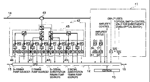
2 5 as shown in Fig. 9. The Raman pump light source unit 42
includes a coupling unit 45, an S+ Raman pump light source unit
46, an S Raman pump light source unit 47, an S+ signal
substitution (additional) Raman pump light source unit 48, and an
S signal substitution Raman pump light source unit 49. The S+
3 o Raman pump light source unit 46 generates S+ band pumping
lights of wavelengths ~,1 and ~, 2 for pumping the S+ band (see
Fig. 5). The unit 46 includes a laser diode LD emitting the pump
light of ~,1, and another laser diode LD emitting the pump light of
~, 2. These laser diodes are controlled by the CPU 12 via digital-
35 to-analog (D/A) converters. The levels of the pumping lights are
monitored by photodiodes via optical taps, and are supplied to the
CPU 12 via analog-to-digital (A/D) converters.
-13-
CA 02433761 2003-07-04
WO 02/056509 PCT/JPO1/00027
The S Raman pump light source unit 47 emits S band
pumping lights of wavelengths ~, 3 and ~, 4 for pumping the S
band (see Fig. 5). The unit 47 has the same structure as the unit
46.
The S+ and S signal substitution Raman pump light
source units 48 and 49 are newly provided according to the first
embodiment of the present invention. The unit 48 generates two
substitute pump lights of wavelengths a, 5 and ~, 6 in the region
between the S band Raman pump wavelengths and the S band
s o signal wavelengths. The unit 48 has the same structure as the
units 46 and 47. The unit 49 generates two substitute pump lights
of wavelengths ~. 7 and ~, 8 in the region between the S band
Raman pump wavelengths and the S band signal wavelengths.
The unit 49 has the same structure as the units 46-8.
The coupler 45 includes seven WDM couplers, and
multiplexes the eight Raman pump lights of ~,1 through a, 8. The
multiplexed Raman pump light is applied to the circulator 43,
which allows it to be propagated through the optical fiber 14 in
the direction opposite to the direction in which signal light is
2 o propagated therethrough (counter-propagating). That is, the
multiplexed pump light thus generated is applied to the signal
light coming from the previous repeater node (not shown in Fig.
9). The circulator 43 is capable of coupling the multiplexed
Raman pump light into the optical fiber 14 even if they are
2 5 spectrally overlapping with the S+lS signal wavelengths.
The CPU 12 controls the pump light source units 46-
49 in accordance with the levels of the S+ and S bands
respectively monitored by the photodiodes 36 and 37. The output
signals of the photodiodes 36 and 37 are applied to the CPU 12
3 o via A/D converters 51 and 52. Further, the CPU 12 receives
information concerning the status of the amplifiers and controls
them, as will be described later. The EEPROM 13 stores
programs executed by the CPU 12, and pre-set parameter values
of the gains of amplifiers (or of the attenuators behind the
35 amplifiers) and the levels of the pump light sources. The
parameter settings for the Raman pump powers and the output
powers of the C and L band channels for the various scenarios
-14-
CA 02433761 2003-07-04
WO 02/056509 PCT/JPO1/00027
(S+ band off, S band off, etc.) are determined at the installation of
the system.
Fig. 10A is a flowchart of a control operation
executed by the CPU 12, and Fig. 10B shows a table describing
possible status changes of S+ and S bands. As shown in Fig. 10B,
16 status changes of the S+ and S bands are possible. Each of the
status changes is identified by serial number #i. For example, for
#i=1, there is no status change, and for #i=4, both the S+ and S
bands change from on to off. For #i=7, the S+ band changes from
Zo on (existence of signal lights) to off (absence of signal lights)
status, and the S band from off to on status. The CPU 12 switches
on/off the Raman pump light source units 48 and 49 in
accordance with the control sequence when a status change of the
S+ and S bands takes place.
Referring to Fig. 10A, the CPU 12 reads the monitor
signals of the S+ and S bands supplied from the photodiodes 36
and 37 via the A/D converters 51 and 52 (step S11). Then, the
CPU 12 determines whether there is a status change of the S+ and
S bands. There is no change for #i=l, 6, 11 and 16. In this case,
2 o the control sequence proceeds to step S 18, which will be
described later. In contrast, if a status change of the S+ and S
bands occurs, the CPU 12 switches off the discrete amplifiers) of
the on-to-off bands) (step S13). Then, the CPU 12 switches off
the substitute Raman pumps) for the off to-on bands) (step S 14).
For case of #i=7, the CPU 12 switches off the amplifier 39 shown
in Fig. 8, and switches off the S signal substitution Raman pump
light source unit 49. At step S 13, depending on the optimum
conditions determined at the installation of the system, the Raman
pumps of the on-to-off bands might also be switched off.
s o Then, the CPU 12 sends, via the control channel 15,
a control signal to the previous repeater node to adjust the C and
L band powers according to the pre-set values of the parameters
stored in the EEPROM 13 for case #i (step S15). The process of
step S 15 may be omitted, if required. The C and L band powers
can be adjusted by controlling the optical amplifiers or the
attenuators behind the amplifiers.
Thereafter, the CPU 12 switches on the substitute
-15-
CA 02433761 2003-07-04
WO 02/056509 PCT/JPO1/00027
Raman pump (s) for the on-to-off bands) (step S 16), and
switches on the discrete amplifiers) of the off to-on bands(s)
(step S 17). For case of #i=7, the CPU 12 switches on the S+
signal substitution Raman pump light source unit 48 shown in Fig.
8, and switches on the optical amplifier 38.
Finally, the CPU 12 receives a control signal from
the next repeater node and adjusts the local C and L band
amplifiers accordingly (step S 18). That is, the amplifier stage 33
of the repeater node 10 shown in Fig. 8 is adjusted by the control
1 o signal sent by the repeater node 20 shown in Fig. 7. It is to be
noted that regardless of status changes, the C and L band
amplifiers (or the attenuators behind these amplifiers) are
adjusted according to the control signal received from the next
repeater node.
The repeater node 20 shown in Fig. 7 operates in the
same manner as the repeater node 10, and therefore a description
thereof will be omitted.
A description will be given of a second embodiment
of the present invention.
2 o Fig. 11 is a block diagram of a WDM transmission
system according to a second embodiment of the present
invention. In Fig. 11, parts that are the same as those shown in
Fig. 7 are given the same reference numbers. Two repeater nodes
100 and 200 employ optical spectrum analyzers (OSA) for
~ 5 monitoring the S+ and S bands. The advantage of the
photodiodes for monitoring the S+ and S bands in the first
embodiment of the present invention is that their response is
much faster than the optical spectrum analyzers. In contrast, the
use of the spectrum analyzers can realize finer control, as will be
3 o described later.
The repeater node 100 is equipped with optical
spectrum analyzers (OSA) 20 and 22, which are coupled with the
optical fiber 14 via optical taps 19 and 21, respectively. The
optical spectrum analyzer 20 monitors the optical spectra of all
35 bands at the input side of the amplifier stage 11 and supplies the
spectral data to the CPU 12. The optical spectrum analyzer 22
monitors the optical spectra of all bands at the output side of the
-l6-
CA 02433761 2003-07-04
WO 02/056509 PCT/JPO1/00027
amplifier stage 11 and supplies the spectral data to the CPU 12.
The amplifier stage 11 and the Raman pump light source unit 42
are configured, for example, as shown in Fig. 8.
Similarly, the repeater node 200 includes optical
spectrum analyzers 24 and 26, which are respectively coupled to
. the input and output sides of the amplifier stage 16 via optical
taps 23 and 25.
Fig. 12A is a flowchart of a control operation of the
CPU 12 of the repeater node 100, and Fig. 12B shows a table
1 o describing possible status changes of S+ and S bands. The
contents of the table shown in Fig. 12B are the same as those of
the table shown in Fig. 10B. The control sequence shown in Fig.
12A includes steps S 12 through S 18 which have been described
with reference to Fig. 10A, and particular steps S20 and S21
resulting from the use of the optical spectrum analyzers. In steps
S 12 through S 18, the spectral data rather than the photodiode
monitor outputs is used.
The CPU 12 executes step S20 at first. At step 520,
the CPU 12 reads input and output spectral data from the optical
2 o spectrum analyzers 20 and 22. In addition, the CPU 12 receives
span input spectral data from the previous repeater node (repeater
node 200), and provides the input spectral data of the repeater
node 100 to the next repeater node. Then, the CPU 12 executes
step 512. If #i=l, 6, 11 or 16, the CPU 12 adjusts the pump
2 5 powers by controlling the laser diodes of the working pumping
power units among the units 46 through 49 via the corresponding
D/A converters. This adjustment refers to the input and output
spectral data and the input spectral data received from the
previous repeater node. The input and output spectral data show
3 o the status of all the channels in each of the bands. Thus, it is
possible to finely adjust the pump powers so that all the channels
can be set at given pre-set levels stored in the EEPROM13.
Further, at step S21, the CPU 12 sends a control signal to the
previous repeater node for adjustment of the signal input powers.
3 5 Then, the CPU 12 executes step S 18, which is followed by step
520.
The first and second embodiments of the present
-17-
CA 02433761 2003-07-04
WO 02/056509 PCT/JPO1/00027
invention may be modified so that three or more Raman pumping
lights can be used. The Raman pump light sources may be a
multiple wavelength pump light source as disclosed, fox instance,
in WO 00/5622. The monitor photodiodes 36 and 37 used in the
first embodiment of the present invention monitor the whole S+
and S bands, respectively. Alternatively, a set of monitor
photodiodes can be combined with a WDM coupler device to
monitor multiple wavelength groups (i.e. subbands) within a band
simultaneously. The monitor photodiodes can be placed behind
s o the amplifiers as well.
A description will be given of other embodiments of
the present invention.
Fig. 13A is a block diagram of a repeater node 10C
according to a third embodiment of the present invention. The
15 repeater node 10C differs from the repeater node 10 in the
position of the optical circulator 43. If the coupling loss of the
WDM coupler 31 is sufficiently low at the short Raman pump
wavelengths, the optical coupler 43 can be placed behind the
WDM coupler 31, as shown in Fig. 13A. This has an advantage
2 o that the loss for the signal lights in the C and L bands in the
transmission line is reduced.
Fig. 13B is a block diagram of a variation of the
repeater node 10C. A repeater node 10D shown in Fig. 13B is
arranged so that the C/L signal lights are counter-propagated with
2 5 respect to the S+/S signal lights. That is, the S+/S Raman pump
lights emitted by the Raman pump light source unit 42 are co-
propagated with the C/L signal lights.
Fig. 13C is a block diagram of a modification 10E of
the repeater node 10C. The Raman pump light source unit 42
3o used in the previously described embodiments of the present
invention is separated into two units 42a and 42b. The unit 42a
corresponds to the combination of the S+ and S Raman pump
light source units 46 and 47 and the associated WDM coupler
shown in Fig. 9. The unit 42b corresponds to the combination of
3 5 the S+ and S signal substitution Raman pump light source units
48 and 49 and the associated WDM couplers shown in Fig. 43.
The S+/S Raman pump light source unit 42a is coupled to the
-18-
CA 02433761 2003-07-04
WO 02/056509 PCT/JPO1/00027
optical fiber 14 in front of the WDM coupler 31 by a WDM
coupler 55. The S+ and S signal substitution Raman pump light
source unit 42b is coupled, by the optical circulator 43, to the
corresponding inner optical fiber so as to be located behind the
WDM coupler 31. With the above arrangement, the coupling
losses for the S+/S Raman pump light can be reduced in
comparison to repeater node 13A.
A variation of the repeater node 10E is illustrated as
a repeater node 10F shown in Fig. 13D. The C/L signal lights are
1 o co-propagated with the Raman pump lights, and are counter
propagated with respect to the S+/S signal lights.
Fig. 14A is a block diagram of a repeater node 10G
according to a fourth embodiment of the present invention. The S
signal substitution Raman pump light source unit 49 is coupled to
the corresponding inner S-signal transmission line so as to be
located behind the WDM coupler 32. The monitor photodiode 36
monitors part of the S signal coming from the optical tap 34. The
unit 49 is controlled based on the status of the S band. The S+
signal substitution Raman pump light source unit 48 is coupled to
2 o the corresponding inner S+-signal transmission line so as to be
located behind the WDM coupler 32. The monitor photodiode 37
monitors part of the S+ signal coming from the optical tap 35.
The unit 48 is controlled based on the status of the S+ band.
Fig. 14B is a block diagram of a variation 10H of the
2 s repeater node 10G. The C/L signal lights are co-propagated with
the Raman pump lights, and are counter-propagated with respect
to the S+/S signal lights.
Fig. 15A is a block diagram of an optical repeater
node 10I according to a fifth embodiment of the present invention,
3 o in which the signal wavelengths extend only to the S band. In this
case, the Raman pump wavelengths can be allocated without
spectrally overlapping with the signal wavelengths. This allows
using a WDM device for coupling the S+ and S signal substitution
Raman pumps into the transmission line. An integrated S Raman
3 5 pump light/S+ and S signal substitution Raman pump light source
unit 42c is coupled to the optical fiber 14 by means of a WDM
coupler 55 located in front of the WDM coupler 31. The Raman
-19-
CA 02433761 2003-07-04
WO 02/056509 PCT/JPO1/00027
pump lights emitted by the unit 42c are counter-propagated with
respect to the S/C/L signal lights. The unit 42c includes the
Raman pump light source units 47, 48 and 49 and the associated
WDM couplers of the coupling unit 45 shown in Fig. 9. The S
band is monitored by the monitor photodiode 37 coupled to the
inner S signal transmission line extending from the WDM coupler
31.
The Raman pump light source unit 42c is controlled
by the status of the S band monitored by the S signal monitor 37
z o under the control of the CPU 12. For example, the Raman pump
light source unit 48 is maintained in the ON state, and Raman
pump light source unit 49 is switched on/off based on the status of
the S band. Alternatively, the S+ and S signal substitution light
source units 48 and 49 may be simultaneously switched on/off
based on the status of the S band.
Fig. 15B is a block diagram of a variation lOJ of the
repeater node 10I. The S band Raman pump light is co-
propagated. The Raman pump light source unit 42 is separated
into the S Raman pump light source unit 47 and an S+ and S
2 o signal substitution Raman pump light source unit 42b. The unit
42b is coupled to the optical fiber 14 forming the transmission
line by a WDM coupler 60 located in front of the WDM coupler
41. The S+ and S signal substitution Raman pump lights are
counter-propagated with respect to the C/L signal lights. The S
2 5 pump light is co-propagated with the C/L signal lights. The S+
and S signal substitution Raman pump light source unit 42b is
controlled by the status of the S band monitored by the monitor
photodiode 37.
Fig. 16A is a block diagram of an optical repeater
s o node 10K, which is another variation of the repeater node 10I. A
WDM coupler 61 is located behind the WDM coupler 31. The S+
and S signal substitution Raman pump light source 42b is coupled
to the inner S signal transmission line by the WDM coupler 61.
The S Raman pump light and the S+/S signal substitution Raman
35 pump lights are counter-propagated with respect to the S/C/L
signal lights.
Fig. 16B is a block diagram of a variation lOL of the
-2 0-
CA 02433761 2003-07-04
WO 02/056509 PCT/JPO1/00027
repeater node 10K. The WDM coupler 61, to which the S+ and S
signal substitution Raman pump light source 42 is coupled, is
located behind the S-band amplifier 38. The S+ and S signal
substitution Raman pump lights axe counter-propagated with
respect to the C/L signal lights. The S Raman pump lights are co-
propagated with the C/L signal lights.
Fig. 17A is a block diagram of an optical repeater
node 17A according to a sixth embodiment of the present
invention. In this embodiment, a pair of optical switches 65 and
s o 66 is used to realize a protection for the C/L band transmission in
the case of an interruption of the S+ and/or S band transmission.
The optical switches 65 and 66 are coupled to respective inner
transmission lines via WDM couplers 75 and 76. Each of the
optical switches 65and 66 allows choosing between two optical
paths. The pair of optical switches 65 and 66 are located in front
of the WDM coupler 31, and selectively connects either the S+/S
Raman pump light source unit 42a or the S+ and S signal
substitution Raman pump light source unit 42b to the transmission
line.
2 o The optical switches 65 and 66 are controlled
together with the S+ and S signal substitution Raman pump light
source unit 42b by the CPU 12, as shown in Fig. 9. The monitor
output status is supplied from the previous repeater node. The
switching control of the optical switches 65 and 66 is the same as
2 5 the aforementioned on/off control of the Raman pump light source
units. That is, the optical switches 65 and 66 are operated in
accordance with the table shown in Fig. 10B.
It is to be noted that the optical switches 65 and 66
do not permit the simultaneous transmission of the S+ and S
3 o signal substitution Raman pump lights and the S+/S signal lights.
Therefore, it is required to perform switching between the S+/S
Raman pump lights and the S+ and S signal substitution Raman
pump lights. This means that only the whole S+ and S band can
be substituted. The Raman pump lights are counter-propagated
3 5 with the signal lights.
An S+lS amplifier stage 62 is used to amplify the
signal lights in the S+ and S bands. A monitor photodiode 63
-21-
CA 02433761 2003-07-04
WO 02/056509 PCT/JPO1/00027
monitors the state of the S+ and S bands. The monitor output for
controlling the S+ and S signal substitution Raman pump light
source unit of the next repeater node is sent to the next repeater
node. The S+/S/C/L signal lights are co-propagated.
Fig. 17B is a block diagram of a variation 10N of the
optical repeater node 10M. A pair of optical switches 67 and 68
is provided in front of the WDM coupler 41. The S+ and S signal
substitution Raman pump light source unit 42b is selectively
coupled to the optical fiber 14 by the switches 67 and 68
1 o controlled by the CPU 12. The C/L signal lights are counter-
propagated with respect to the S+/S signal lights, and are co-
propagated with the S+/S Raman pump lights. The S+ and S
signal substitution Raman pump lights axe counter-propagated
with respect to the C/L signal lights. The monitor output of the
photodiode 63 located behind the S+/S amplifier stage 62 is used
by the CPU 12 to control the switches 67 and 68 and the S+ and S
signal substitution Raman pump light source unit 42b.
Fig. 18A is a block diagram of an optical repeater
node 10P according to a seventh embodiment of the present
2 o invention. An optical switch 69 for selectively coupling the S+
and S signal substitution Raman pump light source unit 42b with
the transmission line is provided behind the WDM coupler 31.
The optical switch 69 is switched on/off by the status of the S+
and S bands monitored by the monitor photodiode 63 under the
2 5 control of the CPU 12. The S+/S Raman pump light source unit
42a is provided in front of the WDM coupler 31 and is coupled to
the optical fiber via the WDM coupler 55. The S+/SlC/L signal
lights are co-propagated, while the S+/S Raman pump lights and
S+/S signal substitution Raman pump lights are counter-
3 o propagated with respect to the signal lights. The CPU 12 controls
the S+ and S signal substitution Raman pump light source unit
42b and the optical switch 69 on the basis of the status of the
S+/S bands monitored by the photodiode 63.
Fig. 18B is a block diagram of a variation 10Q of the
35 repeater node 10P. An optical switch 70 is provided behind the
WDM element 31 as the repeater node shown in Fig. 18A, but is
located in a different position. The S+ and S signal substitution
-22-
CA 02433761 2003-07-04
WO 02/056509 PCT/JPO1/00027
Raman pump light source unit 42b is selectively coupled to the
WDM coupler 41 by the switch 70 based on the status of the S+/S
bands under the control of the CPU 12. The S+ and S signal
substitution Raman pump lights, which are switched based on the
status of the S+/S bands, are counter-propagated with respect to
the C/L signal lights and the S+/S Raman pump lights.
Fig. 19A is a block diagram of an optical repeater
node 10R according to an eighth embodiment of the present
invention. The Raman pump light source unit 48 for substitution
z o for S+ signal lights is coupled behind the WDM coupler 56 by an
optical switch 72. The Raman pump light source unit 49 for
substitution for S signal lights is coupled behind the WDM
coupler 56 by an optical switch 71. The CPU 12 controls the
Raman pump light source unit 48 and the switch 72 on the basis
of the status of the S+ band monitored by the photodiode 37.
Similarly, the CPU 12 controls the Raman pump light source unit
49 and the switch 71 on the basis of the status of the S band
monitored by the photodiode 36. The S+/S Raman pump light
source unit 42a is coupled to the optical fiber 14 via the WDM
2 o coupler 55. The S+/S Raman pump lights and the /S+ and S
signal substitution Raman pump lights are co-propagated, and
counter-propagated with respect to the S+/S/C/L signal lights.
Fig. 19B is a block diagram of a variation 10S of the
optical amplifier 10R. The optical switches 73 and 74 are
2 5 provided behind the optical amplifiers 3 8 and 39, respectively.
The optical switch 73 selectively couples the Raman pump light
source 49 with the WDM coupler 40 based on the status of the S
band under the control of the CPU 12. Similarly, the optical
switch 74 selectively couples the Raman pump light source 48
3 o with the WDM coupler 40 based on the status of the S+ band
under the control of the CPU 12. The S+ and S signal substitution
Raman pump lights are counter-propagated with respect to the
C/L signal lights and the S+/S Raman pump light source unit 42a.
Fig. 25A shows an optical setup for monitoring part
35 of the forward and the backward propagating lights S+S/CL bi-
directional transmission systems by using optical spectrum
analyzers. The forward propagating lights are in the S+ and S
-23-
CA 02433761 2003-07-04
WO 02/056509 PCT/JPO1/00027
bands, and the backward propagating lights are in the C and L
bands. Optical taps 160 and 161 are provided in front and behind
the amplifier stage. A WDM coupler 162 couples parts of
incoming signals of the amplifier stage. A WDM coupler 163
couples parts of outgoing signals. An optical spectrum analyzer
(OSA) 164 connected to the WDM coupler 162 monitors the
power levels of the incoming signals. An optical spectrum
analyzer (OSA) 165 connected to the WDM coupler 163 monitors
the power levels of the outgoing signals. The optical spectrum
s o analyzers 164 and 165 communicate with the CPU 12.
A description will be given of an optical repeater
node according to a ninth embodiment of the present invention.
This repeater node is used in DWDM systems as shown in Fig.
2D. In DWDM systems, impairments due to nonlinear interaction
between neighboring channels can be reduced by channel-
interleaved bi-directional transmission. The channel-interleaving
is illustrated in a graph in Fig. 2D. The channels of the opposite
(forward and backward) propagating directions respectively
illustrated by solid and broken lines are interleaved. At the
2 o amplifier stage, optical circulators are used to separate forward
and backward propagating channels. The amplifier structure for
each direction is similar to that in the aforementioned first
through eighth embodiments of the present invention. The
difference is that all lights in one branch are propagated in the
same direction.
Fig. 20A is a block diagram of an optical repeater
node 100A according to the ninth embodiment of the present
invention, which can be applied to the channel-interleaved bi-
directional S/C/L transmission systems. The repeater node 100A
3 o processes three bands of S, C and L. The repeater node 100A is
coupled to the optical transmission line formed of the optical fiber
14 via optical circulators 43 and 121, which make two amplifier
systems. One of the two systems includes a first optical amplifier
involved in the forward propagation and made up of the
aforementioned components. Similarly, the other system includes
a second optical amplifier having the same structure as the first
optical amplifier. The second amplifier involved in the backward
-24-
CA 02433761 2003-07-04
WO 02/056509 PCT/JPO1/00027
propagation is made up of a WDM coupler 122, a C/L amplifier
stage 123, an S band amplifier 124, an optical tap 125, a monitor
photodiode 126, a S+ and S signal substitution Raman pump light
source unit 127, a WDM coupler 129, an S band Raman pump
light source unit 130, and a WDM coupler 131.
Multiplexed light passes through the circulator 43,
and is applied to the WDM coupler 31. The C/L signal lights are
applied to the C/L amplifier stage 33. The S signal and S-band
pump lights are applied to the S-band amplifier 38. The S+ and S
1 o signal substitution Raman pump source unit 42b is controlled by
the CPU 12 on the basis of the status of the S band in the forward
propagation monitored by the photodiode 37 via the optical tap 34.
The S+ and S signal substitution Raman pump lights are
multiplexed with the amplified S-band signal lights and the C/L
~ 5 signal lights via the WDM coupler 60 and the WDM coupler 41.
Further, the S Raman pump lights are coupled with the output of
the WDM coupler 41 by the WDM coupler 55. Then, the
multiplexed light is sent to the optical fiber 14 via the circulator
121.
2 o Similarly, multiplexed light passes through the
circulator 121, and is applied to the WDM coupler 122. The C/L
signal lights and the S+/S signal substitution Raman pump lights,
if any, are applied to the C/L amplifier stage 123. The S signal
and S-band pump lights are applied to the S-band amplifier 124.
2 5 The S+ and S signal substitution Raman pump source unit 127 is
controlled by the CPU 12 on the basis of the status of the S band
in the backward propagation monitored by the photodiode 126 via
the optical tap 125. The S+ and S signal substitution Raman
pump lights are multiplexed with the amplified S-band signal
3 0 lights and the C/L signal lights via the WDM coupler 128 and the
WDM coupler 129. Further, the S Raman pump lights are
coupled with the output of the WDM coupler 129 by the WDM
coupler 131. Then, the multiplexed light is sent to the optical
fiber 14 via the circulator 43.
3 5 Fig. 20B is a block diagram of a variation 100B of
the optical repeater node 100A shown in Fig. 20A. The S Raman
pump light /S+ and S signal substitution Raman pump light source
-25-
CA 02433761 2003-07-04
WO 02/056509 PCT/JPO1/00027
unit 42c is provided behind the WDM coupler 41 via the WDM
coupler 55. The CPU 12 controls the unit 42c based on the status
of the S band monitored by the monitor photodiode 37 coupled to
the inner S-band forward transmission line extending from the S-
band amplifier 38 via the WDM tap 34. Similarly, an integrated S
Raman pump/S+ and S signal substitution Raman pump light
source unit 130a is provided behind the WDM coupler 129 via the
WDM coupler 131. The CPU 12 controls the unit 130a on the
basis of the status of the S band monitored by the monitor diode
Z o 126 coupled to the inner-S band backward transmission line
extending from the S-band amplifier 124.
Fig. 21 is a block diagram of an optical repeater node
100C according to a tenth embodiment of the present invention.
The device 100C can be applied to the channel-interleaved bi-
directional transmission systems which have the S+/SlC/L bands.
The forward amplifier system includes the aforementioned WDM
coupler 31, the C/L amplifier stage 33, the S+/S amplifier stage
62, the WDM coupler 41, the optical tap 69, the S+/S band
monitor photodiode 63, the S+/S Raman pump light source unit
2 0 42a, the WDM coupler 55, the S+ and S signal substitution
Raman pump light source unit 42b, the WDM coupler 76, and the
optical switches 67 and 68. Similarly, the backward amplifier
system includes the aforementioned WDM coupler 122, the C/L
amplifier stage 123, an S+/S amplifier stage 134, the WDM
2 5 coupler 129, an optical tap 135, an S+/S band monitor photodiode
136, an S+/S Raman pump light source unit 138, a WDM coupler
131, an S+ and S signal substitution Raman pump light source
unit 137, a WDM coupler 132, and optical switches 139 and 140.
The switches 67 and 68 and the Raman pump light
3 o source units 42a and 42b are controlled by the CPU 12 on the
basis of the status of the S+/S bands in the forward propagation
monitored by the photodiode 63. Similarly, the switches 139 and
140 and the Raman pump light source units 137 and 138 are
controlled by the CPU 12 on the basis of the status of the S+/S
35 bands in the backward propagation monitored by the photodiode
136. If the forward S+ and/or S band fails, the S+ and S signal
substitution Raman pump light source unit 42 is selected by the
-26-
CA 02433761 2003-07-04
WO 02/056509 PCT/JPO1/00027
optical switches 67 and 68. Similarly, if the backward S+ and/or
S band fails, the S+ and S signal substitution Raman pump light
source unit 137 is selected by the optical switches 139 and 140.
Fig. 22 is a block diagram of an optical repeater node
100D according to an eleventh embodiment of the present
invention. The first (forward) amplifier system is made up of the
WDM coupler 31, the C/L amplifier stage 33, the S+/S amplifier
stage 62, the optical tap 64, the monitor photodiode 63, the S+
and S signal substitution Raman pump light source unit 42b, the
optical switch 70, the WDM coupler 41, the S+/S Raman pump
light source unit 42a and the WDM coupler 55. The S+ and S
signal substitution Raman pump light source unit 42b controlled
based on the status of the S+/S bands monitored by the
photodiode 63 is selectively coupled to the WDM coupler 41 via
the optical switch 70. The optical switch 70 is controlled by the
CPU 12 to select the S+ and S signal substitution Raman pump
light source unit 42b for protection of the C/L band transmission
in the forward propagation. The S+/S Raman pump light source
unit 42a is coupled to the circulator 121 via the WDM coupler 55.
2 o The second (backward) amplifier system is made up
of the WDM coupler 122, the C/L amplifier stage 123, the S+/S
amplifier stage 134, the optical tap 135, the monitor photodiode
136, the S+ and S signal substitution Raman pump light source
unit 137, the optical switch 140, the WDM coupler 129, the WDM
coupler 131, and the S+/S Raman pump source unit 138. The S+
and 5 signal substitution Raman pump light source unit 137
controlled on the basis of the status of the S+/S bands monitored
by the photodiode 136 is selectively coupled to the WDM coupler
129 via the optical switch 140. The optical switch 140 is
3 o controlled by the CPU 12 to select the S+ and S signal
substitution Raman pump light source unit 137 for protection of
the C/L band transmission in the backward propagation. The
S+/S Raman pump light source unit 138 is coupled to the
circulator 43 via the WDM coupler 131.
3 5 Fig. 23 is a block diagram of an optical repeater node
100E according to a twelfth embodiment of the present invention:
The first (forward) amplifier system is configured as shown in Fig.
-27-
CA 02433761 2003-07-04
WO 02/056509 PCT/JPO1/00027
19B except for the position of the WDM coupler 55 to which the
S+/S Raman pump light source unit 42a is connected. The WDM
coupler 55 of the repeater node 100E is connected to the output of
the WDM coupler 41. The second (backward) amplifier system
has the same structure as the first amplifier system. More
particularly, the second amplifier system includes the WDM
coupler 122, the C/L amplifier stage 123, a WDM coupler 1340, a
WDM coupler 1290, a monitor photodiode 140, an S-band
amplifier 141, an optical tap 142, an S signal substitution Raman
1 o pump light source unit 143, an optical switch 144, a monitor
photodiode 145, an S+-band amplifier 146, an optical tap 147, an
S+ signal substitution Raman pump light source unit 148, an
optical coupler 149, the S+/S Raman pump light source unit 138
and the WDM coupler 129.
If the S band fails, the CPU 12 controls the optical
switch 144 to select the Raman pump light source unit 143 rather
than the S amplifier 141. If the S+ band fails, the CPU 12
controls the optical switch 149 to select the S+ signal substitution
Raman pump light source unit 148 rather than the S+ amplifier
2 0 146.
Fig. 24 is a block diagram of a variation of any of the
optical amplifier units 100 and 100B-100E. If the Raman pump
lights does not spectrally overlap with the signal wavelengths, the
associated Raman pump light sources can be outsides of the
2 5 optical circulators 43 and 121 between which two amplifier stages
150 and 151 are formed. A Raman pump light source unit 152
which emits Raman pump lights that do not spectrally overlap
with the signal wavelengths is coupled to the optical transmission
line via a WDM coupler 153. Similarly, a Raman pump light
3 o source unit 154 which emits Raman pump lights that do not
spectrally overlap with the signal wavelengths is coupled to the
optical transmission line via a WDM coupler 155.
In the optical repeater nodes 100 and 100B-100E, the
monitor photodiodes are used. Rather, optical spectrum analyzers
s 5 may be employed.
Fig. 25B shows an optical setup for monitoring part
of the forward and the backward propagating lights in channel-
-2 8-
CA 02433761 2003-07-04
WO 02/056509 PCT/JPO1/00027
interleaved bi-directional transmission systems by using optical
spectrum analyzers. The forward propagating lights are involved
in even channels, and the backward propagating lights axe
involved in odd channels. Rather than the WDM couplers 162
and 163, optical switches 166 and 167 are used as shown in Fig.
25B.
The present invention is not limited to the
specifically described first through twelfth embodiments,
variations and modifications thereof.
1 o For example, a different number of Raman pumping
lights may be used. The Raman pump sources can be multiple
wavelengths pump sources as disclosed, for instance,
W000105622. Also, wavelength tunable pump light sources may
be used. A single photodiode can be either used to monitor the
s 5 whole optical band, or a set of photodiodes can be combined with
a WDM coupler device to monitor the multiple wavelength
groups (i.e. subbands) within a band simultaneously. The monitor
photodiodes can be placed behind the amplifiers as well.
The present invention includes systems with other
2 o combinations of co-and counter-propagating signal and pump
lights such as a system in which the S+/S pump lights are co-
propagated with the signal lights. The present invention includes
systems which use a different set of bands, such as a system using
S+/C/L bands, as well as systems including the wavelength region
25 beyond the L band (i.e. L+ band).
It is to be noted that the present invention provides a
scheme which allows in-service upgrading of wideband WDM
systems, in which the power transfer from comparatively short
wavelength channels to comparatively long wavelength channels
s o for reliable transmission of the long wavelength channels. If in
such systems first a small number of short wavelength channels is
employed, but the addition of further short wavelength channels
should be kept optional, a provision for later in-service
upgradability has to be made. For this purpose, a small number of
3 5 short wavelengths substitute Raman pumps provide the power to
comparatively longer wavelength channels. Each substitute pump
wavelength replaces a group of short wavelength channels to be
-29-
CA 02433761 2003-07-04
WO 02/056509 PCT/JPO1/00027
installed later.
-30-