Note: Descriptions are shown in the official language in which they were submitted.
CA 02434983 2003-07-16
WO 02/059583 PCT/IE02/00008
A luminescence based sensor
Field of the Invention
The present invention relates to a luminescence based sensor or sensor
configuration of
the type comprising a substrate, an emitting layer having a luminescence
material
which on stimulation is adapted to transmit luminescence into the substrate
and a
detector for detecting light subsequently transmitted out of the substrate.
Back~:round to the Invention
There has been increasing application of luminescence based sensors in areas
such as
environmental monitoring, biochips, DNA chips, bioluminescence,
chemiluminescence
and many others. The sensors typically comprise a substrate having a
luminescence
emittex in optical contact therewith. The emitter may of itself transmit
luminescence into
the substrate or may require to be activated in some way, either by incident
light or by
some chemical reaction. There are various forms of luminescence:
phosphorescence
which is long lived light transmission, fluorescence which is short lived,
chemiluminescence where two chemicals react and finally bioluminescence.
Within the
present specification the term "luminescence" is intended to encompass all
such forms
of luminescence. Many chemical sensors and biosensors are based on the
luminescence
emitted from thin layers or patterned arrays of fluorophores deposited on a
dielectric
interface such as a waveguide surface or a transparent substrate. One of the
key issues in
these sensors is the efficiency of the luminescence collection.
A typical configuration in many luminescence-based sensor applications
involves a thin
luminescent film or spot deposited onto a planar substrate. An example of such
a
configuration is Figure 1, which shows a substrate 100 having a luminescent
spot 110
deposited thereon. A detector 120 is provided under the substrate 100 and is
adapted to
detect light 130 that is transmitted by the spot into the substrate and which
passes out of
the substrate. It will be noted that the detector is positioned directly under
the spot 110
CA 02434983 2003-07-16
WO 02/059583 PCT/IE02/00008
2
so as to detect light that passes normally ( i.e. undeviated by refraction at
the interfaces)
through the substrate. Within the present specification the element containing
the
substrate and the luminescent layer or spot will be referred to as the sensing
element or
sensor chip. The sensor chip is considered to be designed independently of the
sensor
system in which it is to be incorporated.
A majority of luminescence-based sensor systems employ rather inefficient
techniques
for the collection of luminescence emitted by a thin sensing film or molecules
attached
to a surface. A number of authors have developed new ways of dealing with the
issue of
to low luminescence intensity emitted by systems under study. Liebermann et
al. [T.
Lieber-mann and W. Knoll. Surface plasmon field-enhanced fluorescence
spectroscopy.
Colloids and Surfaces, A: Physicochemical and Engineering Aspects 171:115-130,
2000.] exploited the enhancement of the amplitude of the excitation light in
the close
vicinity of a metal surface provided by the efficient excitation of the
surface plasmon
15 wave. Blair ~ Chen [S. Blair and Y. Chen. Resonant-enhanced evanescent-wave
fluorescence biosensing with cylindrical optical cavities. Applied Optics,
40(4):570-
581, 2001 ] showed that luminescence of molecules can be enhanced by the use
of planar
cylindrical resonant optical cavities.
2o It is also known to incorporate metal coatings or metal nanoparticles into
a sensor and
the incorporation of these materials can have a very positive influence on the
intensity
of luminescence emitted by molecules located in their close vicinity.
Enhancement of
the quantum yield in the order of 100-1000 has been reported. Although these
developments are certainly valuable for the improvement of the performance of
the
25 luminescence-based chemical sensors and bio-sensors, they do not address
the issue of
efficiency of the luminescence collection.
Polerecky L et al (Applied Optics 39 (22): 3968-3977Aug 12000) have described
a
theory of radiation from dipoles embedded inside an arbitrary multilayer
system . They
3o derive explicit expressions for the angular distribution of the
electromagnetic field and
intensity radiated by the dipole into the surrounding media. Using this
theoretical
analysis they conclude consequences for optimisation of optical chemical
sensors and
CA 02434983 2003-07-16
WO 02/059583 PCT/IE02/00008
3
biosensors based on luminescence emission, specifically that as a large
proportion of the
luminescence is radiated into the higher refractive index substrate and due to
total
internal reflection at the glass/air interface is guided along the glass-
slide, better results
should be provided by detecting the luminescence at the edge of the glass-
slide.
Although this technique facilitates the detection of the modes that normally
propagate
along the glass slide towards the edge, the detection is riot optimised, as
only those
modes propagating within a narrow angular range Oc~ , as shown in Figure 2,
are
detected. In order to maximise this fraction, detectors would have to be
placed all
around the substrate which is not feasible in most practical applications.
There therefore exists a need for a method and sensor for detecting a
luminescence
signal that is based on the understanding that a large proportion of
luminescent light that
is radiated into a substrate to which the material is attached is not
detected.
Object of the Invention
It is an object of the present invention to provide a sensor configuration
which is
adapted to detect light that is radiated into a substrate at high angles. It
is also an object
of the present invention to provide a method of detecting the presence of
analytes using
sensor configurations that are optimised for detecting light that is radiated
into a
substrate at such high angles. .
Summary of the Invention
Accordingly the present invention provides a luminescent sensor configuration
comprising a substrate having a first refractive index, a luminescent material
having a
second refractive index and a detector. The sensor is adapted for use in a
medium
having a third refractive index; the third refractive index being less than
the second
refractive index and the second refractive index being less than the first
refractive index,
The substrate is adapted to specifically redirect light radiated into the
substrate by the
luminescent material at angles which are less than the critical angle of the
luminescent
CA 02434983 2003-07-16
WO 02/059583 PCT/IE02/00008
4
material/substrate interface and greater than the critical angle of the
medium/substrate
interface, the light being redirected out of the substrate and towards a
detector.
Desirably at least two distinct portions of luminescent material are provided
each
portion being optically coupled to the substrate. The substrate is typically
adapted to
redirect the light emitted by each portion towards the detector such that the
light
received at the detector from a first portion is spatially independent from
the light
received at the detector from a second portion.
The redirection of light by the substrate is preferably effected by at least
one optical
redirection element provided at either upper or lower surfaces of the
substrate.
In a first embodiment the at least one optical redirection element is adapted
to redirect
the light using total internal reflection.
Such a configuration may comprises a plurality of optical redirection
elements, each
element comprises a frusto-conical structure raised above the upper surface of
the
substrate, each frusto-conical structure having side walls and an upper
surface,
luminescent material being carried on the upper surface of the structure, and
wherein
2o light emitted by the material into the structure is internally reflected by
the side walls of
the structure and directed towards a detector positioned beneath the
substrate.
It may alternatively comprises at least one ridge raised above the upper
surface of the
substrate and extending along the upper surface of the substrate, the ridge
having side
walls and an upper surface, luminescent material being earned on the upper
surface of
the ridge, and wherein light emitted by the material into the ridge is
internally reflected
by the side walls of the ridge and directed towards a detector positioned
beneath the
substrate.
The side walls of the redirection element are typically vertically displaced
from the
uppex surface of the redirection element at an angle substantially equivalent
to one
CA 02434983 2003-07-16
WO 02/059583 PCT/IE02/00008
quarter the sum of the critical angles of the luminescent material/substrate
interface and
the medium/substrate interface.
In an alternative embodiment the at least one optical redirection element is
adapted to
5 redirect the light using refraction.
In such an embodiment the at least one optical redirection element may
comprise a
prism optically coupled to a lower surface of the substrate, the prism being
adapted to
receive light incident on the lower surface of the substrate and redirect that
light
l0 sidewardly towards a detector.
It may alternatively comprise a plurality of prisms, each prism being
associated with a
unique spot on the upper surface of the substrate, such that light emitted by
a spot is
received within its associated prism and re-directed towards a detector.
The prism is typically optically coupled to the lower surface of the substrate
and the
prism has the same refractive index as the substrate to which it is optically
coupled.
In a further embodiment the at least one optical redirection element is
adapted to
redirect the light using diffraction. Typically this comprises a difFractive
optical element
provided at the lower surface of the substrate.
In an alternative embodiment the lower surface of the substrate is
structurally
configured to both reflect and refract light radiated into the substrate, the
reflection and
refraction of the light effecting a redirection of light towards a detector.
In such an
embodiment the lower surface is typically such as to provide a first surface
on which
light emitted from the material and incident thereon is refracted out of the
substrate and
towards the second surface, which reflects the light which is incident thereon
towards
the detector.
In yet a further embodiment the optical redirection element comprises a
refractive index
barrier extending inwardly of the substrate, the refractive index barrier
being
CA 02434983 2003-07-16
WO 02/059583 PCT/IE02/00008
6
substantially perpendicular to the lower surface of the substrate such that
light incident
on the barrier from the luminescent material is reflected downwardly and out
of the
substrate. Typically the refractive index barrier comprises an annular slot
having side
walls, the side walls extending inwardly of the substrate, the walls being
substantially
perpendicular to the lower surface of the substrate such that light that is
incident on the
walls from the luminescent material is reflected dowriwardly and out of the
substrate.
'The walls may be provided with a reflective coating so as to improve the
reflectivity of
the surfaces of the walls. Such a reflective coating is typically formed from
metal
1o particles or material deposited on the walls.
In yet a further embodiment the redirection of light by the substrate is
effected by
providing the substrate with non-parallel upper and lower surfaces, the angle
of the
upper and lower surfaces being such that the Light emitted by the luminescence
material
1s is incident on the surfaces at angles greater than the critical angle of
the
substrate/medium interface, thereby effecting a propagation of light along a
critical axis
of the substrate towards a detector.
The sensor configuration is typically configured such that the detector
detects light
20 radiated into the substrate by the luminescent material at angles which are
not less than
the critical angle of the luminescent material/substrate interface and greater
than the
critical angle of the medium/substrate interface, in addition to the light
radiated within
the angular range.
25 The detector is desirably a CMOS or CCD type detector.
The luminescent material is desirably sensitive to an analyte with which the
sensor is
intended to be used. The presence of an analyte in the medium with which the
sensor is
used effects a luminescence of the material and said luminescence is detected
at the
30 detector.
CA 02434983 2003-07-16
WO 02/059583 PCT/IE02/00008
7
The sensor configuration may be initially provided with a bio-recognition
element, the
bio-recognition element being sensitive to and adapted to couple with any
compatible
biological sample in the medium with which the sensor is used. Once this
coupling has
been effected the sensor may be exposed to a luminescent tag which couples to
the
coupled biological sample/bio-recognition element so as to radiate
luminescence into
the substrate.
The invention additionally provides a luminescence sensor comprising a
substrate
adapted to receive incident light emitted from a luminescence material
optically coupled
1o thereto, a detector adapted to detect the light emitted into the substrate
and wherein the
substrate is specifically adapted to outwardly direct light defined by the
substrate
confined (SC) modes of the incident light from the substrate and towards the
detector.
The structural geometry of the substrate at the upper or lower surfaces
thereof is
desirably such as to the outwardly direct the light defined by the SC modes.
The invention additionally provides an assay tool for use in detecting the
presence of a
substance in a medium, the tool comprising a substrate having at least one
optical
redirection element at either upper or lower surfaces of the substrate, the
optical
2o redirection element adapted, to specifically redirect light radiated into
the substrate by a
luminescent material at angles which are less than the critical angle of the
luminescent
material/substrate interface and greater than the critical angle of the
medium/substrate
interface, the light being redirected out of the substrate and towards a
detector.
The invention may additionally provide a method of enhancing the luminescence
capture from an assay tool, the method comprising the step of providing an
assay tool
having a substrate with at least one optical redirection element at either
upper or lower
surfaces of the substrate, the optical redirection element adapted to
specifically redirect
light radiated into the substrate by a luminescent material at angles which
are less than
3o the critical angle of the luminescent material/substrate interface and
greater than the
critical angle of the medium/substrate interface, the light being redirected
out of the
substrate and towards a detector.
CA 02434983 2003-07-16
WO 02/059583 PCT/IE02/00008
8
In a further embodiment the invention provides a luminescence-based sensor of
the type
comprising a substrate mounting an emitting layer transmitting luminescence
into the
substrate and a detector for measuring some of the trapped light in the
substrate
subsequently transmitted out of substrate characterised in that the substrate
is so
configured to internally direct the trapped light through an exit surface to
the detector.
By configuring the substrate externally i.e. by altering its shape, it is
possible to ensure
that the trapped light is directed to an exit surface and is not totally
internally reflected
within the substrate. The detector could, for example, be a photo detector
which may be
a CCD camera which can be located below or above the substrate. The invention
arises
out of an analysis of the radiation of dipoles placed within a thin dielectric
layer coated
on a higher refractive index substrate which reveals that the luminescence
exhibits
strong spatial anisotropy with significantly greater amounts of luminescence
radiated
within a certain interval of angles.
Accordingly the invention provides a range of configurations which exploit the
findings
that a significantly greater amount of luminescence is radiated into the
higher refractive
index substrate at angles greater than the critical angle of the
substrate/superstrate
interface, and that in most substrates, most of the luminescence is radiated
into the
substrate and is trapped there and ensures that the luminescence, instead of
being
trapped within the substrate, is transmitted out of it for subsequent
detection and
measurement.
In one embodiment of the invention, the luminescence-based sensor is so
arranged that
the trapped light is directed through the exit surface substantially normally
thereto.
In another embodiment of the invention, at least either the upper surface
mounting the
emitter or the lower surface of the substrate is not planar. If planar, the
surfaces are not
parallel.
CA 02434983 2003-07-16
WO 02/059583 PCT/IE02/00008
9
In a further embodiment of the invention, the interfaces of the substrate are
so
configured that the internal reflection at the interface on which the trapped
light
impinges is substantially prevented and allows the light to be transmitted
through the
substrate.
In yet another embodiment of the invention, the interfaces of the substrate
are so
configured that the trapped light is reflected from at least one interface
before being
directed out of.the substrate to the detector.
1o These and other features of the present invention will be better understood
with
reference to the following drawings
Brief Description of the Drawings
Figure 1 is a schematic showing a sensor device according to the prior art,
15 Figure 2 shows a configuration adapted for edge detecting light passing out
through the
edges of a substrate,
Figure 3 shows the angular properties of luminescence radiated from a small
luminescence spot on a glass substrate; the substrate being surrounded by air
below and
by air above ( Figure 3a) and by water above (Figure 3b),
20 Figure 4.1(a) is a graph showing the relative optical power carried by the
AT, ST, SC
and EW modes as a function of the thickness t1 of the luminescent spot, while
the
refractive index of the layer is constant an equal to n1 =1.43 and the spot is
covered by
air,
Figure 4.1(b) is equivalent to Figure 4.1(a) but when the spot is covered with
water and
25 the AT modes are substituted by WT modes,
Figure 4.2(a) is a graph showing the relative optical power carried by the AT,
ST, SC
and EW modes as a function of the refractive index n1 of the luminescent spot,
while the
thickness of the layer is constant an equal to t1 = 1:5~,, and the spot is
covered by air,
Figure 4.2(b) is equivalent to Figure 4.2(a) but when the spot is covered by
water, and
3o the AT modes are substituted by WT modes,
CA 02434983 2003-07-16
WO 02/059583 PCT/IE02/00008
Figure 5 is a schematic diagram of an ideal detection system (IDS)
characterised by a
numerical aperture NA = sin 9~0 , where 9~o is the cone angle associated with
the cone
of light entering the system,
Figure 6 is a graph showing the efficiency of the detection of optical power
carried by
5 various types of modes radiated by the luminescent spot as plotted for the
ideal situation
of Figure 5 as a function of its numerical apertuxe NA,
Figure 7a is a plan view of a substrate according to the invention carrying a
sensor array,
Figure 7b is a perspective view of a substrate according to the invention
having a
plurality of ridges formed thereon,
1o Figure Sa is a side view of a sensox from the array of Figure 7a,
Figure 8b is a detailed view of the sensor of Figure 8a,
Figure 8c is graph showing the fraction of the luminescence detected by an
ideal
detection system as a function of its numerical aperture NA,
Figure 9 is a side view of an alternative embodiment of a sensor according to
the present
invention,
Figure 10 is a side view of a further embodiment of a sensor according to the
present
invention,
Figure 11 is a side view of a further embodiment of a sensor according to the
present
invention,
Figure 12 is a side view of a further embodiment of a sensor according to the
present
invention,
Figure 13 is a side view of a further embodiment of a sensor according to the
present
invention,
Figure 14 is a side view of a further embodiment of a sensor according to the
present
invention,
Figure 15 is a modification to the embodiment of Figure 14,
Figure 16 is a plan view of the embodiment of Figure 15,
Figure 17 shows typical examples of the images of the luminescence detected
from 4
spots deposited onto a polystyrene chip according to the embodiment of Figure
8, and
3o Figure 18 shows additional images to those of Figure 17.
CA 02434983 2003-07-16
WO 02/059583 PCT/IE02/00008
11
Detailed Description of the Drawings_
Figures 1 and 2 have been described with reference to the prior art.
The present invention utilises light that is transmitted into the substrate by
a luminescent
material at high incident angles. Using conventional prior art apparatus such
light has
propagated within the substrate and although it has been noted that a portion
of it passes
out through edge portions of the substrate a method and apparatus that is
specifically
adapted to detect such modes of light has hereintobefore not been described.
Figure 3 shows an example of a sensing element. The same reference numerals
will be
used for the same components in the various embodiments. It consists of a
"thick" glass
slide substrate 100 (refractive index ns =1.515, thickness ~ 1mm) on top of
which a
small spot of luminescent material 110(refractive index n~ = 1:43) is
deposited. It will be
appreciated that the material is optically coupled to the substrate. By the
term optically
coupled it will be appreciated by those skilled in the art that it encompasses
a plurality
of different arrangements including, but not limited to:
i. luminescent molecules directly bound to or adsorbed on substrate,
ii. luminescent molecules indirectly attached to substrate via one or more
linker molecules (such as in a sandwich assay),
iii. luminescent molecules entrapped/contained within a thin film, for example
a
polymer or sol-gel matrix, coated on substrate.
The thickness ti of the Iayer forming the spot is assumed to be uniform and in
the range
of hundreds of nanometers. Furthermore, for simplicity, the size of the spot
is assumed
to be small compared to the size of the area of the detection system which is
used to
detect the luminescence produced by the spot. The latter restriction is
assumed only to
ensure that the luminescent spot "appears" to the detector as a spot rather
than as an
area over which the radiated intensity would have be integrated. Consequently,
the
lateral (x-y) dimensions do not have to be considered and only the angular
dependence
of the radiated intensity needs to be taken into account in the following
analysis. The
CA 02434983 2003-07-16
WO 02/059583 PCT/IE02/00008
12
luminescent spot is assumed to be covered by the environment, which is either
air (na =
1.0) or water (nW =133). The slide is surrounded by air from below.
The predicted angular distribution of the luminescence emerging from the small
luminescent spot deposited on the glass substrate is shown in Figure 3. The
graphs (a)
and (b) correspond to the situations where the environments or media covering
the spot
are air and water, respectively. In both graphs, the solid line 300 and the
dashed line 310
correspond to the thickness of the luminescent spot equal to t1 = O.S~, and t1
=1.5 ~,,
respectively, where ~, is the luminescence wavelength. Luminescence that can
be
detected by the detector placed above the glass substrate is schematically
shown by the
arrow 320. Luminescence within this angular distribution is typical of the
luminescence
that has traditionally been used within sensor systems. As can be seen from
the
displacement of the luminescence as shown in the solid 300 or dashed 310 lines
located
in air or water above the glass substrate, the amount of luminescence radiated
into the
environment covering the spot is relatively small.
The situation is similar when the detector is placed below the glass
substrate. Due to
reflections taking place at the bottom glass/air interface, the light
impinging at this
interface is transmitted to air only if the incident angle lies within the
angular range
8 E (-9~,~) , where 9~S = arcsin(rca /ns) ~ 413° is the critical angle
of the substrate
(glass)/air interface. This light is schematically depicted by the dashed
arrows 330. Due
to the refraction, the light propagating inside the substrate at angles 8 E(-
~5,8~) is
partially transmitted into the air under the substrate at angles 9 E (-
90°,90°) . The solid
300 and dashed 310 lines within the angular range B E (-6~',B~J demonstrate
that the
amount of luminescence transmitted to air below the glass substrate is also
relatively
small. These arrows indicate the portion of the light that is traditionally
detected using
prior art apparatus.
The light propagating inside the substrate at angles greater than the critical
angle ~ is
totally reflected at the lower substrate/air interface. If the environment
covering the slide
is air, as shown in Fig. 3(a), this light is also totally reflected at the
upper layer/air
CA 02434983 2003-07-16
WO 02/059583 PCT/IE02/00008
13
interface and is effectively trapped (or confined) within the waveguiding
glass substrate.
If the environment above the slide is water, as shown in Fig. 3(b), the part
of the light
propagating in the substrate at angles B E (6~ , B~ S ) and 8 E (-B~ ,-B~ S J
is partially
transmitted into water and partially reflected back to the substrate.
Furthermore, the part
of light propagating at 8 E (6~ S ,90° J and 8 E (-8~ S a 90° )
is totally reflected at the upper
layer/water interface. In any case, due to the relation B~S > 9~ , the light
exhibiting the
enhanced intensity is always trapped inside the substrate due to the total
internal
reflection at both the upper and lower interfaces. This light has previously
not been
captured in prior art arrangements and has propagated normally within the
substrate
until it escapes out the edges of the substrate.
This analysis clearly explains why large values of the luminescence capture
efficiency
cannot be achieved by the conventional detection technique employing detection
above
or below the substrate. It is mainly due to the fact that conventional
techniques facilitate
the detection only of the low-intensity modes generated by the luminescent
spot. The
analysis also demonstrates that a higher capture efficiency could be achieved
if the more
intense modes, i.e., those propagating at angles B E (B~S,B~ ) and 8 ~ (-8~ ,-
8~ ) are
detected. In these expressions, B~ is equal either to 9~ or B~S depending on
whether
the environment covering the luminescent spot is air or water, and 9~ is the
critical
2o angle of the layer/substrate interface.
To simplify the subsequent discussion, the following terminology is
introduced. The
luminescence directly transmitted to air or water above the substrate will be
called "the
air-transmitted" or "the water-transmitted luminescence". The corresponding
modes of
the electromagnetic field will be called "the air-transmitted" or "water-
transmitted
' modes" or, shortly, AT or WT modes. The luminescence radiated into the
substrate at
angles 8 E (-9~ , ~ ) , which is eventually transmitted into air under the
substrate, will
be called "the substrate-transmitted luminescence". The corresponding modes
will be
called "the substrate-transmitted (ST) modes". The luminescence radiated into
the
3o substrate at angles 8 E (9~S , e~ J and B E (-9~S ,-e~ ) , which is trapped
or confined
CA 02434983 2003-07-16
WO 02/059583 PCT/IE02/00008
14
inside the substrate, will be called "the substrate-confined luminescence".
The
corresponding modes will be called "the substrate-confined (SC) modes". The
luminescence propagating at angles 9 E ~9~ ,90° > and B E (-B~ ,-
90° ) will be called
"the evanescent-wave (EW) luminescence". The corresponding modes will be
called
"the evanescent- wave (EW) modes". Although it is also trapped (confined)
inside the
substrate, this name reflects better the character of the field corresponding
to these
modes, which is evanescent in the luminescent layer. This is qualitatively
different from
the SC modes, whose field is propagating (i.e., described by a harmonic
function) inside
the luminescent layer.
To provide quantitative analysis of the improvement in the luminescence
capture
efficiency that could be achieved by employing the detection of the SC modes
in
accordance with the present invention, the total optical power carried by the
AT/WT
modes, ST modes, SC modes and the EW modes may be calculated and compared.
Such a comparison is shown in Figures 4 and 5. The graphs (a) and (b) in both
figures
correspond to the situations where the environments covering the luminescent
spot are
air and water, respectively.
Figure 4.1 shows the relative power carried by the modes as a function of the
thickness
t1 of the luminescent layer, where the refractive index of the layer is
assumed to be
constant and equal to n~ = 1.43. The total power carried by all the modes is
proportional
to the thickness t1. However, as can be seen from both graphs in Figure 4.1,
the relative
fraction of the power carried by each of the modes remains practically
constant over a
substantially large interval of t1. The notable variation is exhibited by the
SC modes
which gain the relative power at the expense of the EW modes. This is due to
the fact
that for greater values of t1 the coupling between the more distant regions of
the
luminescent layer from the substrate and the EW modes is weaker (due to the
finite
penetration depth of the evanescent field). The graph (a) in Figure 4.1
indicates that the
SC modes carry approximately 66 % of the total luminescence radiated by the
spot
3o when the spot is covered by air. This number is somewhat smaller when the
luminescent
spot is covered by water ( approx. 50 %), which is caused by the increase of
the fraction
CA 02434983 2003-07-16
WO 02/059583 PCT/IE02/00008
of luminescence radiated into water by means of the WT modes, as follows from
the
comparison of the dashed lines in graphs (a) and (b).
Although these numbers might not seem too large when compared to the fractions
of the
5 power carried by the AT modes (approx.15 %), WT modes (approx. 30 %) or the
ST
modes (approx.15 %), it is important to realise that the SC modes are
"localised" in a
narrower angular range ( ~ 8 = 9~ - ~ ~ 30° and O B = 8~ - B~ S ~
10° for the situations
where the spot is covered by air and water, respectively) than the other
modes, which
are propagating in the full range 8 E ~-90°,90° J . To
facilitate the detection of the full
1o power carried by the AT, WT, or ST modes, one would have to use a
detection~system
with the value of the numerical aperture equal to 1, which is difficult to
achieve. On the
other hand, the large power carried by the SC modes could be detected using a
detection
system with a low value of the numerical aperture (not exceeding sin
15° ~ 0.26 fox
0B = 30° or sin 5° ~ 0.09 . for ~8 =10° ).
Figure 4.2 shows the relative power carried by the modes as a function of the
refractive
index n1 of the luminescent layer, where the layer thickness is assumed to be
constant
and equal to t1 = 1.5~,. It can be seen that the power carried by the SC modes
increases
rapidly as n1 approaches the value of the substrate refractive index (n5 =
1.515). This is
2o mainly due to the shift of the critical angle, which converges to
90° as n1 approaches ns.
As in the case discussed above, the fraction of the power carried by the SC
modes is
generally smaller when the environment covering the luminescent spot is water.
This is
again due to the fact that the luminescence radiated into water has higher
intensity, as
follows from the comparison of the dashed lines in the graphs (a) and (b) of
Figure 4.2.
Nevertheless, Figure 4.2 demonstrates that a greater fraction of the energy
carried by the
SC modes is obtained when the refractive index of the luminescent layer is
chosen as
close to that of the substrate as possible. The above analysis considers the
total optical
power carried by the various types of modes radiated from the luminescent
spot. This
3o means that in order to make these quantities comparable as measures of the
luminescence capture efficiency, a detection system which is able to capture
all the
CA 02434983 2003-07-16
WO 02/059583 PCT/IE02/00008
16
power carxi.ed by the particular modes would have to be employed. For example,
in case
of.the AT, WT or ST modes, the detection system would have to be able to
detect light
beams propagating in the cone with the cone angle of 90°, i.e.,
characterised by the
numerical aperture NA =1.
In order to provide a better quantitative comparison .between the different
types of
modes, it is necessary to consider them in the context of the detection
system. This can
be done by evaluating the detected power as a function of the numerical
aperture of the
detection system. In the following analysis, an ideal detection system, which
is depicted
in Figure S, is considered. It is assumed to be placed directly below or above
the
luminescent spot, i.e., its axis (dashed-dotted line) is perpendicular to the
surface of the
substrate and intersects the luminescent spot. The system employs an ideal
lens (L)
which redirects the beams corresponding to the AT/WT and ST modes to the
detector
array (DA). S denotes the substrate containing the luminescent spot (LS), as
shown in
Fig. 3. ,
One of the most important quantities characterising a detection system is its
numerical
aperture (NA). It is related to the value of the cone angle 9~o by NA = sin
8~~ . The fact
that the system is ideal means that all the light propagating within the cone
characterised
by the cone angle ~~~ = arcsin NA is detected and converted to the signal
proportional to
the total power carried by the corresponding modes. At this stage, only the
AT, WT and
ST modes are considered. Figure 6 shows the efficiency of detection of the AT,
WT and
ST modes as a function of the numerical aperture of the ideal detection system
described
above. The lines marked by (a) and (w) correspond to the situations where the
luminescent spot is covered by air and water, respectively.
luminescent spot covered by
air water
AT modes: ~ 13 % WT modes: ~ 31 %
ST modes: ~ 16% ST modes: ~ 14%
SC modes: = 66% SC modes: ~ 50%
EW modes: .:; 5% EW modes: ~ 5%
CA 02434983 2003-07-16
WO 02/059583 PCT/IE02/00008
17
Table 1: Relative values of total optical power carried by specified modes
calculated for a sensor chip depicted in Fig. 3. The thickness and refractive
index of the
luminescent spot for which these values were calculated are tl = 1.5 ~, and
nl=1.43,
respectively.
It can be seen from the graph of Figure 6 that the relative values of the
detected optical
power, which are listed in Table 1, can be achieved only with a detection
system whose
numerical aperture is equal to unity. For NA < 1, the capture efficiency
decreases
rapidly. For example, it falls below 5 % for NA < 0.5. This means that even an
ideal
1o detection system cannot detect more than 5 % of the total power radiated by
the
luminescent spot when its numerical aperture is lower than 0.5. This makes the
SC
modes attractive because they carry more power which is concentrated within a
narrower angular range, thus allowing fox a greater capture efficiency at a
lower
numerical aperture of the detection system.
It will be appreciated by those skilled in the art that the above numerical
analysis has
been conducted with reference to specific exemplary values of the refractive
index and
the thickness of the luminescent layer and other material involved. The
present
invention is not intended to be limited to any such specific example and it
will be
further appreciated that a similar analysis with qualitatively similar results
is obtainable
for any other set of parameters.
It will be further appreciated from the previous discussion that the modes
that we are
mainly interested in, in accordance with the present invention, are those
modes radiated
into the higher refractive index substrate at angles B that satisfy the
following inequalities:
(1) B~S < 8 < B~
where B~S is the critical angle of the environment/substrate interface and B~
is the
3o critical angle of the luminescent layer/substrate interface. It will be
appreciated that the
term "environment" is intended to define the medium such as air or water where
the
CA 02434983 2003-07-16
WO 02/059583 PCT/IE02/00008
18
sensor is used. If the refractive indices of the substrate, luminescent layer
and
environment are denoted as ns, n1 and ne, respectively, the critical angles
are calculated
as:
(2a) B~ = arcsin(ne /ns) ,
(2b) 9~ = arcsin(n~ / nS )
The inequality (1) requires that the refractive indices must satisfy the
relation
1o (3) ne < n1 < ns .
It should be noted that the enhancement effects that are exploited according
to the
present invention occur if the refractive indices characterising the materials
satisfy the
relation (3).
Using an appreciation of the mechanism of propagation of a luminescence
radiated from
a luminescent spot or layer by the SC modes, the present invention provides
means by
which these modes may be detected so as to improve luminescence capture
efficiency.
The present invention provides in preferred embodiments for a modification of
the
2o geometry of the top or bottom interface or surface of the substrate so as
to re-direct the
SC modes towards a detector placed either above or below the substrate. This
modification can be achieved by a plurality of different mechanisms, examples
of which
will be illustrated in the following sections. It will be appreciated that by
employing
macroscopic or microscopic structures at the top or bottom substrate interface
that is
possible, using for example means of reflection, refraction or diffraction to
change the
direction of propagation of the SC modes. Such a redirection may be adapted to
effectively direct the SC modes towards a suitably orientated detector.
The following examples are presented as exemplary embodiments of the present
invention and are not intended to limit the invention to such embodiments.
CA 02434983 2003-07-16
WO 02/059583 PCT/IE02/00008
19
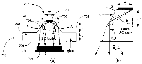
Figures 7 and 8 show a sensor device indicated generally by the reference
numeral 700,
which comprises a substrate 702 coated with a plurality of individual portions
of
luminescent material 703 sensitive to an analyte species, below which is
mounted a
photo detector 704 for collecting the luminescence emerging from the
substrate. The
detector 704 mounted below the substrate 702 comprises a CCD camera. The
substrate
702 has an upper surface 705 and a lower surface 706. In the embodiment of
Figure 7a,
each portion of luminescent material 703 is in the form of a spot on a frusto-
conical
structure 707, whereas in the embodiment of Figure 7b the luminescent material
extends
along an upper surface of a number of ridges 710 provided on the upper surface
of the
substrate.
As shown in Figure 7a, the upper surface 705 may be so configured to have a
plurality
of frusto conical structures 707 or protuberances, each structure having side
walls 708
and an upper surface 709. The structures typically protrude project from the
upper
surface 705 of the substrate. The upper surface of the structure 709 is
adapted to carry
the spots 703.
As shown in Figure 7b, the upper surface of the substrate is provided with a
plurality of
ridges 710, each ridge having side walls 711 extending upwardly from the upper
surface
of the substrate and having an upper surface 712 which carries or to which a
layer of
luminescent material 703 is optically coupled.
On stimulation, the luminescent material 703 will radiate light substantially
in
accordance with the configuration illustrated in Figure 3. The SC modes which
have an
angle of propagation above the critical angle initially hit the sides wall 708
and in
accordance with total internal reflection are reflected from the inner surface
of the side
walls downwardly towards the lower surface of the substrate 706 where they
exit arid
are detected by the detector 704. This is illustrated in Fig. 8. It will be
appreciated that
in order to specifically direct the SC modes downwardly towards the detector,
thereby
outcoupling them from their normal path of propagation within the substrate
702, that
the angle of displacement a of the side walls 708 of the conical surface of
the structure
707 has to be so chosen as to ensure that the light is redirected and
reflected from it
CA 02434983 2003-07-16
WO 02/059583 PCT/IE02/00008
straight downwards through the lower surface 706 to the detector 704. This
conical
surface is at the angle a to the vertical.
The principle behind this design is the total internal reflection of the SC
modes radiated
5 from the luminescent spot by the tilted interface A (708). The advantage of
this
configuration is two-fold. Firstly, the total internal reflection at this
interface is feasible
fox all the SC modes and can be achieved by a proper choice of the tilt angle
. Secondly,
the redirected SC modes impinge on the bottom interface of the substrate at
angles close
to 0° which guarantees that a large fraction of the power is
transmitted out of the
10 substrate towards the detector. The disadvantage of this configuration is
that the top
interface of the substrate needs to be modified which makes it not directly
compatible
with systems employing pure planar architecture.
Although it is not intended to limit the present invention to any specific
theory or
15 analysis it may be considered that the substrate containing the luminescent
spot is made
of glass (ns = 1.515) and surrounded by air (na =1.0) both from the top and
bottom. The
analysis can be, however, extended to any other set of parameters.
As is shown in Fig. 3(a), the SC modes propagate in the glass substrate at
angles
20 8 E ~9°S , 8~ ~ , where 6~ = arcsin(~aQ / hs ) ~ 413° and ~~
= arcsin(~~ / ns ) ~ 70.7° are
the critical angles of the air/substrate and layer/substrate interfaces,
respectively. The
choice of the tilt angle can be based on various criteria. In this analysis,
the requirement
is that the central SC beam, i.e., the light corresponding to the SC modes
propagating in
the glass at an angle B~entre = (e~s + 9~ ) / 2 , is redirected straight down
upon total
internal reflection from the interface A, as shown in Fig. 8b.
Simple geometrical analysis implies that the angles 8 and B, i.e. the
propagation angles
of the light before and after the total internal reflection from the interface
A, are related
by
8+B=2a
CA 02434983 2003-07-16
WO 02/059583 PCT/IE02/00008
21
Due to the fact that ~ _ ~~entre and ~ = 0 for the central SC beam, the tilt
angle can be
calculated as
a = 2 e~en~er = 4 (e~ + B~ ) ~ 28°
Using this value of alpha, the beams corresponding to the SC modes propagating
at
angles BeS and 9~ before the total internal reflection at the interface A are
propagating
at angles B~S = 4 B~ / 2 and 8~ _ -~ B~° / 2 respectively, where
~e~° _ (B~ -8~) ~ 29.4°
This means that the SC modes propagate within the angular range of
oe'a oe'°
. 8 E - 2~ , 2' ~ ~-14.7° ,14.7°
.immediately after the total internal reflection at the interface A.
When the refraction at the bottom interface of the substrate is considered,
the SC beam
propagating in the glass substrate at an angle 8 is found to be propagating in
air below
the substrate at an angle 8 as shown in Fig. 8(b). These angles are related by
the Snell
law, i.e.,
~cQ sin ~ = hs sin
Consequently, the SC modes propagate in air below the substrate within the
angular
range of
~8~a ~elu
B E - 2~ , 2' ~ ~-22.6° ,22.6°
This implies that all the power carried by the SC modes can be captured by a
detector
whose numerical aperture corresponds to the cone angle of approximately
22.6° , i.e.
numerical aperture NA approximately 0.38. It will be appreciated that the
performance
of the sensor configuration or apparatus of the present invention gives an
order of
magnitude improvement within the range 0.4 to 0.6.
CA 02434983 2003-07-16
WO 02/059583 PCT/IE02/00008
22
After the propagation characteristics of the luminescence have been found, it
is possible
to make a comparison between the luminescence capture efficiency of the
conventional
detection technique (see Figs.1) and that of the improved configuration
depicted in Fig.
8a. Figure 8c shows the efficiency of the luminescence detection as a function
of the
numerical aperture of the ideal detection system. The dashed and dash-dotted
lines
correspond to the conventional technique employing detection of the
luminescence
radiated from the luminescent spot by means of the AT and ST modes,
respectively. The
solid line corresponds to the configuration employing frustrated cones (see
Figs. 8).
It will be appreciated from an analysis of Figure 6 that the conventional
detection
technique can capture a maximum of approximately 15 % of the total emitted
luminescence. However, this is possible only with a detection system
characterised by
NA =1. On the other hand, the detection system with NA of approximately 0.38
is able
to detect approximately 63 % of the total luminescence radiated from the
luminescent
spot if the improved detection configuration is employed to redirect the SC
modes
towards the detector. This clearly represents a substantial improvement. As
can be seen
from Fig. 8c, the efficiency of the luminescence capture achieved by the
improved
configuration does not increase above 63 % for NA > 0.38. This is because only
the SC
modes are considered in the evaluation of the capture efficiency (see solid
line). In
reality, however, the detector placed below the substrate would also detect
the ST modes
in addition to the SC modes. Consequently, the capture efficiency of such a
system
would continue increasing above NA = 0.38. This is depicted by the dotted
curve, which
is obtained as a sum of the solid (SC modes) and dash-dotted (ST modes)
curves.
When the luminescence capture efficiency of the conventional detection
technique at
NA of approx. 0.38 is evaluated, a value of only approximately 1.8 % is found
(see Fig.
8c). This means that for this given value of NA, the improved configuration
provides
approximately 35-fold increase in the luminescence capture efficiency. This
remarkably
large increase makes the configuration very attractive, despite the fact that
it is not
entirely compatible with the planar architecture.
CA 02434983 2003-07-16
WO 02/059583 PCT/IE02/00008
23
In the design of the configuration with improved luminescence capture
efficiency, the
tilt angle, a , plays an important role. As mentioned earlier, its evaluation
can be based
on various criteria. Once this angle is determined, the values of the other
parameters
characterising the configuration, such as W, h and t (see Fig. 8a), can be
found from
simple geometry. Subsequently, the values can be proportionately scaled up or
down.
The scaling factor is primarily determined by the target application and the
technology
employed in the fabrication process.
1o If the parameters characterising the properties of the substrate,
luminescent spot or the
environment covexing the spot are different, the geometrical parameters of the
configuration with improved luminescence capture efficiency would change.
However,
these parameters can easily be found by adopting the above analysis to such a
system.
Following the same steps as those discussed above, the tilt angle together
with the
angular range can be found. Furthermore, the dependence of the luminescence
capture
efficiency on NA, which would be similar to that shown in Fig. 8c, can be
evaluated in
order to determine the optimum design parameters.
Fig. 9 illustrates an alternative construction of substrate, identified by the
reference
2o numeral 900, in which parts similar to those described with reference to
the previous
drawings are identified by the same reference numerals. In this embodiment,
the
substrate 900 has an upper surface 705 which is planar and a low configured
surface
901(a) arid 901(b) which, by refraction and reflection, directs the light onto
the detector
704, the light being first refracted through a lower surface 901(a) and then
reflect from
the lower surface 901(b) to the detector which is not shown, but will be
appreciated as
being positioned below the substrate. It will be appreciated that
configurations such as
this embodiment employ a combination of refractive and reflective elements at
the
bottom interface of the substrate. Total internal reflection at the bottom
interface of the
substrate is avoided by configuring the plane of the interface so as to
decrease the angles
of incidence of the SC modes to values lower than the critical angle.
CA 02434983 2003-07-16
WO 02/059583 PCT/IE02/00008
24
This plane, through which the SC modes are refracted and transmitted outside
the
substrate, is denoted by A. If it is required that the detection takes place
under the
substrate below the luminescent spot, an additional air-substrate interface,
denoted by B,
can be incorporated in order to reflect the SC modes. A particular advantage
of this
configuration is that the top interface containing the luminescent spot is
planar. This is
important if the system is required to be compatible with another system
employing a
planar architecture. Furthermore, the orientation of the plane A is designed
so as to
ensure that'the SC modes impinge on the plane A at angles close to 0, i.e.,
almost at
normal incidence. This is important because the fraction T of the power
transmitted
1o through this plane, which is determined by T ~ 1- I(ns - ha ) J (fas + ha
)~2 , is large (T is
approximately 96 %). Although the tilted interface A provides efficient out-
coupling of
the SC modes outside the substrate, the modes propagate in air immediately
after the
interface A at large angles. This would make it difficult to detect the SC
modes
effectively by a detector placed under the substrate. For this reason the
reflecting
interface B is provided in the configuration. Its function is to redirect the
SC modes
towards the detector. However, a high reflectivity of this interface cannot be
achieved if
it is determined solely by the differences between the refractive indices of
the substrate
and air. For example, for ns = 1.515 and na = 1.0, the reflectivity is
approximately
(fas - nu ) J (~zs + rau )~2 ~ 4 % for the incident angles up to approx.
50° and is still less
then approx. 50 % for angles as high as 80°. Therefore, unless the
reflectivity of the
interface B is increased, e.g., by depositing a reflective metal layer, the
poor reflectivity
of this interface makes the redirection and thus the detection of the SC modes
under the
substrate rather ineffective.
Fig.10 illustrates a constriction of a sensor system or configuration, in
which parts
similar to those described with reference to previous drawings are identified
by the same
reference numerals. In this embodiment, there are mounted on the lower surface
706,
macroscopic redirection elements 1016. The redirection elements, which in the
example
3o of Figure 10 are shown in the form or a individual prisms optically coupled
to the lower
surface 706 of the substrate, are adapted to outcouple the SC modes which are
incident
CA 02434983 2003-07-16
WO 02/059583 PCT/IE02/00008
on the lower surface 706 from their normal path of propagation within the
substrate such
that they are redirected downwardly and sidewardly towards the detector 704.
Another way of out-coupling the SC modes from the substrate and redirecting
them
5 towards the detector placed under the substrate is to use diffraction. For
example, if a
diffractive element, such as a grating or a more general diffractive optical
element
(DOE), is placed in the position where the SC modes hit the bottom interface
of the
substrate, the light propagated by means of the SC modes can be out-coupled
and
redirected towards the detector at the same time.
Such a configuration is shown in the embodiment of Fig.11, where there is
illustrated
another substrate having microscopic redirection elements 1121 provided
thereon. It
will be appreciated that the macroscopic 1016 and the microscopic redirection
elements
1121 of the substrates of Figure 10 and Figure 11 will typically be integrally
formed
therein.
It will be appreciated that with either of these two latter configurations,
the bottom of
the substrate is so constructed that the luminescence emerging from the layer
can be
redirected by the structure as desired. When the structure is macroscopic,
redirection is
by way of refraction and when it is microscopic such as a diffraction grating
or a general
diffractive optical element, the redirection is defined by diffraction.
Referring now to Fig.12, there is illustrated an alternative construction of
the substrate,
identified by the reference numeral 1225 carrying on its upper surface 705 a
dense array
of spots 703. The substrate 1225 is placed on an index matching prism 1226
having
lower surfaces 1227 and 1228 which are so designed that the emitted light
which is
being emitted from each spot within a narrow angular range, impinges on the
lower
surface 1227 of the prism 1226 substantially at right angles thereto so as to
impinge
against the detector 704. It will be appreciated that another detector could
be placed on
3o the side of the prism against and behind the other lower surface 1228. It
will be
appreciated that the substrate 1225 and prism 1226 may be integrally moulded.
CA 02434983 2003-07-16
WO 02/059583 PCT/IE02/00008
26
Referring to Fig.13, there is illustrated an alternative construction of
substrate,
identified by the reference numeral 1330, having a planar upper surface 705
and a planar
lower surface 1306 which are so configured as to direct and reflect the light
internally
until it is directed out to the detector 704 at one end thereof. By shifting
the angle of
incidence of the light at the interfaces to angles greater than the critical
angle, there will
be little loss of the luminescent light, propagating along the critical axis
of the structure,
than would be achieved if both the upper and lower surface were parallel to
one another
as would have been detected at the edge of traditional sensing devices.
Referring to Fig. 14, there is illustrated an alternative construction of
substrate,
identified by the reference numeral 1440 in which parts similar to those
described with
reference to the previous drawings are identified by the same reference
numerals. The
substrate 1440 has a lower surface 1441 carrying an inwardly directed annular
slot 1442
carrying vertical surfaces 1443 which provide for reflection. The efficiency
of such a
configuration of the substrate may be improved by providing reflective
coatings, such as
a metal coating, on the vertical surfaces. It will also be appreciated by the
person skilled
in the art that the slot in effect forms a refractive index barrier which
serves to reflect the
light incident thereon, and that alternative configurations such as a doping
of specific
2o portions of the substrate so as to provide an equivalent reflective barner
could also be
implemented
Referring now to Figs.15 and 16, there is illustrated a still further
construction of
substrate, identified by the reference numeral 1550, substantially similar to
the substrate
1440 except that the substrate has a lower surface 1544 intermediate the slots
1442
which provides even better transmission of the re-directed light.
With the present invention, it has been found that the configurations
according to it
improve luminescence collection efficiency compared with standard techniques
based
on direct detection above or below the substrate, it has been found that with
the present
invention, significantly increased amounts of light have been collected that
as
heretofore been possible.
CA 02434983 2003-07-16
WO 02/059583 PCT/IE02/00008
27
Experimental Results
In order to quantify the improvement provided by the embodiments of the
present
invention, an experimental set up utilising the arrangement described in
Figure 8 was
established. The luminescent spots were made of a sol-gel derived thin film
doped with
a luminescent ruthenium complex (ruthenium tris diphenyl phenanthroline or
Ru(dpp)3),
which is characterised by the refractive index n1 =1.425. The chip was made
from
polystyrene whose refractive index over the range of wavelengths corresponding
to the
1o emission spectrum of the doped sol-gel is approximately ns =1.590. The
environment
covering the spots was air (na = 1.0). Using these parameters, the critical
angles 8~ and
9~ which play a fundamental role in the design, could be calculated. Their
respective
values are 9~S = 63.7° and 6~S = 39.0°. 'The value of the tilt
angle a, was calculated to be
approximately 26°. The configuration was designed in the axially
symmetric form, and
the values of the dimensions w and h were w = 1 mm and h =1 mm. The chip
incorporated a 2 X 4 array of frustrated cones on a single substrate.
The thin luminescent spots were deposited onto the substrate using a stamp
fabricated
from poly-dimethylsiloxane (PDMS).
Two independent experiments using two independently prepared samples were
carried
out in order to measure the improvement provided by the configuration
employing
frustrated cones. The first experiment employed a CCD camera, and the second
used a
detection system using a CMOS camera.
It can be seen, from Figure 17, that there are two distinct intensity profiles
visible in
both images. The ring-like profiles correspond to the luminescence produced by
the
spots which were deposited at the top of the frustrated cones. In particular,
the light
impinging the detector array at the area of the bright ring (R) corresponds to
the SC
modes of the luminescence radiated by the spot. On the other hand, the less
evident grey
spots (S) correspond to the ST modes of the light produced by the luminescent
spots
CA 02434983 2003-07-16
WO 02/059583 PCT/IE02/00008
28
deposited onto an unmodified planar substrate, i.e., they correspond to the
images of the
luminescence intensity obtained by the conventional or traditional detection
technique.
The intensity corresponding to the ST modes radiated from the spots deposited
at the
top of the frustrated cones is also visible, namely in the inner area of the
rings (spots
denoted by S ~. It can be seen that there is some non-uniformity in the
intensity
distribution across the image. For example, using the image in Fig.17(a), the
right ring
appears to be brighter than the left one and the top spot seems to be less
bright than that
at the bottom. Similar features can be observed from the image in Fig.17(b).
This is due
to non-uniformity of the intensity profile of the blue excitation light
illuminating the
luminescent spots, which could not be avoided due to an inherently divergent
and
spatially anisotropic character of the light produced by a LED. Furthermore,
the spots S
appear to be greater in size than the spots S'. This is due to a greater
physical size of the
luminescent spots deposited onto the planar substrate than those deposited at
the top of
the frustrated cones, which was caused solely by the stamping method utilised.
To estimate the improvement of the luminescence capture efficiency, the
images, such
as those shown in Figure 17 were analysed. In the analysis the effects of both
the non-
uniformity of excitation and the size of the luminescent spot were taken into
account.
Details of this analysis are summarised below for the independently obtained
experimental data.
CCD-based experiment
The analysis of the experiment employing the CCD camera is based on the image
shown
in Fig.18(a). In the first step of the analysis, the total intensities
detected in the areas
denoted by C1-C4, A2 and A4 were obtained. The circular areas C1 and C3
represent
the intensity profiles of the ST modes emitted by the luminescent spots
deposited onto
the unmodified (planar) substrate and detected by the CCD camera. The circular
areas
C2 and C4 represent the same but for the spots deposited at the top of the
frustrated
cones. The annulus areas A2 and A4 represent the intensity profiles of the SC
modes
which are emitted by the luminescent spots deposited at the top of the
frustrated cones
CA 02434983 2003-07-16
WO 02/059583 PCT/IE02/00008
29
and redirected towards the detector. The corresponding total intensities are
listed in
Table 2, step 1.
total
intensity
[norm.
units]
step C1 . C2 C3 C4 A2 A4 C2+A2 C4+A4
1 1.15 0.438 0528 0.257 4.30 2.87 4.74 3.13
2 0.010 0.010 0.091 0.072 - - - -
3 1.15 0.438 0.589 0.359 4.30 4.01 4.74 4.37
4 0.289 0.438 0.239 0.359 430 4.01 4.74 4.37
1.00 1.52 0.830 1.24 14.9 13.9 16.4 15.1
'
52 0.660 1.00 0550 0.82 9.82 9.16 10.8 9.98
53 1.21 1.83 1.00 1.50 18.0 16.8 19.8 183
54 0.805 1.22 0.666 1.00 12.0 11.2 13.2 12.2
Table 2: Analysis of the data provided by the image in Fig.18 (a).
5
In the next step of the analysis, the non-uniformity of the illumination by
the blue light
was taken into account. This was done by requiring that the intensity in the
centre of the
circular areas C2-C4 be the same for each circular area. This was based on the
assumption that all the spots deposited either at the top of the frustrated
cones or onto
to the unmodified (planar) substrate have equal thickness. Indeed, in that
case, the
intensities of the luminescence radiated at an angle B = 0 should be equal.
The
intensities corresponding to the centre of the circular areas C1-C4 are listed
in Table 2,
step 2. The intensities corresponding to all considered areas and obtained by
this re-
normalisation step are listen in Table 2, step 3. In the next step of the
analysis, physical
dimensions of the luminescent spots was taken into account. This was done by
measuring the diameter d of the circular areas C1-C4 which corresponded to the
diameter of the physical spots. The following values, in arbitrary units, of
the diameters
were found: dcl =140, dc2 = 70, d~ =110, d~ = 70. The intensities obtained
after this
re-normalisation step are listed in Table 2, step 4.
In order to write the values in a form which would be more convenient for
further
comparison, the values obtained in the step 4 were re-normalised so that the
intensities
CA 02434983 2003-07-16
WO 02/059583 PCT/IE02/00008
' 30
corresponding to the circular areas C1-C4 would be unity. These final values
are listed
in Table 2.2, steps 5I- 54 , respectively.
It will~be noted that although the background intensity needed to be
considered in these
calculations, it was found to be zero and thus did not affect the final
numerical values
listed in Table 2. On the other hand, as can be seen from the image in
Fig.17(b), the
background signal was quite substantial in the experiments using the CMOS
camera and
thus had to be considered in the calculations.
CMOS-based experiments
The analysis of the experiment employing the CMOS camera is based on the image
shown in Fig.18(b). As mentioned above, the background signal has to be
considered in
the analysis of the image shown in Fig. 17(b). Three regions of the same area
are
defined in the image, namely a ring-like region (R) which corresponds to the
intensity of
the luminescence emitted from the spot deposited at the top of the frustrated
cone, a
circular spot (S) which corresponds to the same but originating from the spot
deposited
onto the unmodified (planar) substrate, and a circular region "bkg" which
provides a
measure for the background signal. All the regions are of the same area and so
the total
intensities obtained in the following calculations are directly comparable.
The total
intensities measured in these regions are listed in Table 3, step 1.
total intensity [norm. units]
step S R bkg
1 0.946 2.12 0.837
2 0.109 1.28 0.000
3 1.00 11.8 0.000
Table 3: Analysis of the data provided by the image in Fig.18(B).
To enable direct comparison between the intensities emitted from the spot
deposited at
the top of the frustrated cone (area R) and that deposited on the planar
(unmodified)
substrate (area S), the intensity of the background (area "bkg") had to be
subtracted.
The values of the intensities after this re-normalisation step are listed in
Table 3, step 2
CA 02434983 2003-07-16
WO 02/059583 PCT/IE02/00008
31
In order to write the values in a form which would be more convenient for
further
comparison, the values obtained in Step 2 where re-normalised so that the
intensity
corresponding to the area S would be unity. The final values are listed in
Table 3, step 3.
It can be seen from Tables 2 and 3 that the enhancement of the detected
intensity
provided by the configuration employing frustrated cones (see Fig. 8) is
substantial. In
particular, when the total intensity detected from a spot deposited at the top
of the
frustrated cone is compared to the intensity emitted by means of the ST modes,
an
l0 enhancement by a factor of approximately 11-12 is obtained (see the values
in columns
C2 +A2 and C4 +A4 and the values in columns C2 and C4 in Table 2 at lines 52
and 54 ,
respectively). When the total luminescence intensity detected from a spot
deposited at
the top of the frustrated cone is compared to the total intensity detected
from a spot
deposited on an unmodified (planar) substrate, an enhancement of approximately
15-20
x5 is found (see the values in columns C2 +A2 and C4 +A4 and the values in
columns C1
and C3 in Table 2.2 at lines 51 and 53 , respectively). This factor is
slightly lower
(approximately 12) when the data in Table 3 is used. This difference is
attributed to
possible discrepancies in the thickness of the spots deposited at the top of
the frustrated
cones and those deposited onto the unmodified (planar) substrate, the latter
being
20 approximately 1.5 times thinner than the former, due to the imperfection of
the stamping
method used.
These results are experimental evidence of the level of improvement of the
luminescence capture efficiency that can be achieved by employing the
structure with
25 frustrated cones in comparison to the efficiency provided by the
conventional detection
technique. Even though the improvement does not reach as high values as those
corresponding to the ideal situation, the 10-12 fold increase in the detected
intensity
clearly demonstrates how attractive the improved configuration is. It is
believed that this
improvement factor could be further increased by providing better quality (in
terms of
30 the surface roughness) of the side walls of the structure.
CA 02434983 2003-07-16
WO 02/059583 PCT/IE02/00008
32
It will be appreciated that the substrate and sensor configuration of the
present invention
provide enhanced luminescence capture from materials. Such enhancement has
many
applications in sensors such as environmental monitoring, biochips, DNA chips,
bioluminescence, chemiluminescence and many others. The improvement enables a
lower detection of substances in a medium than is available using traditional
of
conventional techniques. Typical implementations of the present invention will
include
assay kits or tools which comprises a plurality of sensing elements, each
elements being
adapted to detect one or more specific substances. It will be further
appreciated by those
skilled in the art that the application of the luminescence material that is
used with the
substrate of the present invention may be achieved in any of a number of
different ways,
and may differ for specific application or purposes. Furthermore it will be
appreciated
that the sensitivity of the material may be chosen specifically for particular
applications,
as some materials are sensitive for the presence of certain material or
samples but not
for others.
The words "comprises/comprising" and the words "having/including" when used
herein
with reference to the present invention are used to specify the presence of
stated
features, integers, steps or components but does not preclude the presence or
addition of
one or more other features, integers, steps, components or groups thereof.
Similarly, the
words "upper", "lower", "above", "below" etc., are not intended to limit the
application
of the present invention to such physical configurations.