Note: Descriptions are shown in the official language in which they were submitted.
CA 02435964 2003-07-24
WO 02/061814 PCT/GB02/00445
METHOD OF MANUFACTURING OPTICAL DEVICES
AND RELATED IMPROVEMENTS
FIELD OF INVENTION
This invention relates to a method of manufacturing of optical devices, and in
particular, though not exclusively, to manufacturing integrated optical
devices or
optoelectronic devices, for example, semiconductor optoelectronic devices such
as laser diodes, optical modulators, optical amplifiers, optical switches,
optical
detectors, and the like. The invention further relates to Optoelectronic
Integrated
1 o Circuits (OEICs) and Photonic Integrated Circuits (PICs) including such
devices.
BACKGROUND TO INVENTION
Quantum Well Intermixing (QWI) is a process which has been reported as
providing a possible route to monolithic optoelectronic integration. QWI may
be
performed in III-V semiconductor materials, eg Aluminium Gallium Arsenide
(AIGaAs) and Indium Gallium Arsenide Phosphide (InGaAsP), which may be
grown on binary substrates, eg Gallium Arsenide (GaAs) or Indium Phosphide
(InP). QWI alters the band-gap of an as-grown structure through interdiffusion
of
elements of a Quantum Well (QW) and associated barners to produce an alloy of
2 o the constituent components. The alloy has a band-gap which is larger than
that of
the as-grown QW. Any optical radiation (light) generated within the QW where
no QWI has taken place can therefore pass through a QWI or "intermixed" region
of alloy which is effectively transparent to the said optical radiation.
2 5 Various QWI techniques have been reported in the literature. For example,
QWT
can be performed by high temperature diffusion of elements such as Zinc into a
semiconductor material including a QW.
QWI can also be performed by implantation of elements such as silicon into a
QW
CA 02435964 2003-07-24
WO 02/061814 PCT/GB02/00445
semiconductor material. In such a technique the implantation element
introduces
point defects in the structure of the semiconductor material which are moved
through the semiconductor material inducing intermixing in the QW structure by
a high temperature annealing step.
Such QWI techniques have been reported in "Applications of Neutral Impurity
Disordering in Fabricating Low-Loss Optical Waveguides and Integrated
Waveguide Devices", Marsh et al, Optical and Quantum Electronics, 23, 1991,
s941 - s957, the content of which is incorporated herein by reference.
A problem exists with such techniques in that although the QWI will alter
(increase) the band-gap of the semiconductor material post-growth, residual
diffusion or implantation dopants can introduce large losses due to the free
carrier
absorption coefficient of these dopant elements.
A further reported QWI technique providing intermixing is Impurity Free
Vacancy
Diffusion (IFVD). When performing IFVD the top cap layer of the III-V
semiconductor structure is typically GaAs or Indium Gallium Arsenide (InGaAs).
Upon the top layer is deposited a silica (SiO~) film. Subsequent rapid thermal
2 o annealing of the semiconductor material causes bonds to break within the
semiconductor alloy and Gallium ions or atoms - which are susceptible to
silica
(Si02) - to dissolve into the silica so as to leave vacancies in the cap
layer. The
vacancies then diffuse through the semiconductor structure inducing layer
intermixing, eg in the QW structure.
IFVD has been reported in "Quantitative Model for the Kinetics of
Compositional
Intermixing in GaAs-AlGaAs Quantum-Confined Heterostructures", by Helmy
et al, IEEE Journal of Selected Topics in Quantum Electronics, Vol 4, No 4,
July/August 1998, pp 653 - 660, the content of which is incorporated herein by
2
CA 02435964 2003-07-24
WO 02/061814 PCT/GB02/00445
reference.
It is an object of at least one aspect of the present invention to obviate or
at least
mitigate at least one of the aforementioned disadvantages/problems in the
prior art.
It is also an object of at least one aspect of the present invention to
provide an
improved method of manufacturing an optical device using an improved QWI
process.
1 o SUMMARY OF INVENTION
According to a first aspect of the present invention, there is provided a
method of
manufacturing an optical device, a device body portion from which the device
is
to be made including a Quantum Well (QW) structure, the method including the
step of processing the device body portion so as to create extended defects at
least
in a portion of the device portion.
Each extended defect may be understood to be a structural defect comprising a
plurality of adjacent "point" defects.
2 o Preferably said step of processing the device body portion comprises
performing
a plasma etch on the device body portion. Preferably and advantageously the
said
step of performing a plasma etch on the device body portion may be performed
in
a sputterer. In said step of sputtering from the device body portion a
magnetic
field may be provided around the device body portion. In said step of
sputtering
2 5 from the device body portion, a magnetron sputterer may be used.
In said step of performing a sputter etch on the device body portion a
(reverse)
electrical bias may be applied across an electrode upon which the device body
portion is provided so as to provide a "pre-etch" or cleansing of the device
body
3
CA 02435964 2003-07-24
WO 02/061814 PCT/GB02/00445
portion. Preferably the sputter-etch is carried out for between 0.5 and 10
minutes
at a power between 300 and 750 W, at a sputter pressure between 1 and 5 ptn
Hg.
The method may include the preferred step of depositing a dielectric layer on
at
least one other portion of the device body portion. The dielectric layer may
therefore act as a mask in defining the at least one portion. The method may
also
include the subsequent step of depositing a further dielectric layer on the
dielectric
layer and/or on the at least one portion of the device body portion.
1 o Advantageously the dielectric layer and/or further dielectric layer may be
deposited by use of a sputterer. Alternatively, the dielectric layer and/or
the
further dielectric layer may be deposited by a deposition technique other than
by
use of a sputterer, eg Plasma Enhanced Chemical Vapour Deposition (PECVD).
By either of these deposition techniques at least one low damage dielectric
layers
is provided which does not substantially affect an adjacent portion of the
device
body portion.
The dielectric layer or layers may beneficially substantially comprise silica
(Si02);
or may comprise another dielectric material such as Aluminium Oxide (A1203).
Preferably, the sputterer includes a chamber which may be substantially filled
with
an inert gas such as argon, preferably at a pressure of around 2 microns of
Hg, or
a mixture of argon and oxygen, eg in the proportion 90% / 10%.
2 5 The steps) of depositing the dielectric layers) may comprise part of a
Quantum
Well Intermixing (QWI) process used in manufacture of the device. The QWI
process may comprise Impurity-Free Vacancy Disordering (IFVD).
Preferably, the method of manufacture also includes the subsequent step of
4
CA 02435964 2003-07-24
WO 02/061814 PCT/GB02/00445
annealing the device body portion including the dielectric layer at an
elevated
temperature.
It has been surprisingly found that by performing the plasma etch on the
device
body portion as a step in a QWI technique such as IFVD, preferably by use of a
sputterer, damage induced extended defects appear to be introduced into the at
least one portion of the device body portion; the at least one portion may,
for
example, comprise at least a part of a top or "capping" layer. It is believed
that the
damage arises due to breakage of bonds in the capping layer before annealing,
eg
2 o the application of thermal energy by rapid thermal annealing, thereby
inhibiting
transfer of Gallium from the at least one portion, eg into the further
dielectric
layer.
Preferably the method of manufacture also includes the preceding steps of:
z 5 providing a substrate;
growing on the substrate:
a first optical cladding layer;
a core guiding layer including a Quantum Well (QW) structure; and
a second optical cladding layer.
The first optical cladding layer, core guiding layer, and second optical
cladding
layer may be grown by Molecular Beam Epitaxy (MBE) or Metal Organic
Chemical Vapour Deposition (MOCVD).
2 5 In a preferred embodiment the method may comprise the steps of
depositing the dielectric layer on a surface of the device body portion;
defining a pattern in photoresist on a surface of the dielectric layer and
lifting off at least part of the photoresist so as to provide the dielectric
layer on said
at least one other portion of the device body portion.
5
CA 02435964 2003-07-24
WO 02/061814 PCT/GB02/00445
In said preferred embodiment, the method may also include the step of
depositing
the further dielectric layer on a portion of the surface of the device body
and on a
surface of the dielectric layer prior to annealing.
In said preferred embodiment, the dielectric layer may comprise an intermixing
cap; while the at least one portion of the device body portion and/or the
further
dielectric layer may comprise an intermixing suppressing cap. The thickness of
the dielectric layers) may be between 10 and 1000 nm. More preferably, the
1 o thickness of the dielectric layers may be 200 or 300 nm.
A subsequent annealing step may occur at a temperature of between 700 and
1000°C for between 0.5 and 5 minutes, more preferably between 800 and
1000°C
and in one embodiment at substantially 900°C for around 1 minute.
According to a second aspect of the present invention there is provided a
method
of manufacturing an optical device, a device body portion from which the
device
is to be made including a Quantum Well (QW) structure, the method including
the
step of performing a plasma etch on the device body portion. Preferably the
step
2 0 of performing a plasma etch on the device body portion is carried out
using a
sputterer.
According to a third aspect of the present invention there is provided an
optical
device fabricated from a method according to either of the first or second
aspects
2 5 of the present invention. The optical device may be an integrated optical
device
or an optoelectronic device.
The device body portion may be fabricated in a III-V semiconductor materials
system. In a most preferred embodiment the III-V semiconductor materials
5
CA 02435964 2003-07-24
WO 02/061814 PCT/GB02/00445
system may be a Gallium Arsenide (GaAs) based system, and may operate at a
wavelengths) of substantially between 600 and 1300 nm. Alternatively, in a
less
preferred embodiment the III-V semiconductor materials system may be an
Indium Phosphide based system, and may operate at a wavelengths) of
substantially between 1200 and 1700 nm. The device body portion may be made
at least partly from Aluminium Gallium Arsenide (AlGaAs) and / or Indium
Gallium Arsenide (InGaAs), Indium Gallium Arsenide Phosphide (InGaAsP),
Indium Gallium Aluminium Arsenide (InGaAlAs) andlor Indium Gallium
Aluminium Phosphide (InGaAIP).
The device body portion may comprise a substrate upon which are provided a
first
optical cladding layer, a core guiding layer, and a second optical cladding
layer.
Preferably the Quantum Well (QW) structure is provided within the core guiding
layer. The core guiding layer, as grown, may have a smaller band-gap and
higher
refractive index than the first and second optical cladding layers.
According to a fourth aspect of the present invention there is provided an
optical
integrated circuit, optoelectronic integrated circuit (OEIC), or photonic
integrated
circuit (PIC) including at least one optical device according to the third
aspect of
2 o the present invention.
According to a fifth aspect of the present invention there is provided a
device body
portion ("sample") when used in a method according to either the first or the
second aspects of the present invention.
According to a sixth aspect of the present invention there is provided a wafer
of
material including at least one device body portion when used in a method
according to either of the first or second aspects of the present invention.
CA 02435964 2003-07-24
WO 02/061814 PCT/GB02/00445
According to a seventh aspect of the present invention there is provided a
plasma
etching apparatus when used in a method according to the second aspect of the
present invention. Preferably the sputtering apparatus is a sputterer, which
may
be a magnetron sputterer.
According to an eighth aspect of the present invention there is provided use
of a
sputtering apparatus in a method according to either of the first or second
aspects
of the present invention.
s o BRIEF DESCRIPTION OF DRAWINGS
Embodiments of the present invention will now be described, by way of example
only, and with reference to the accompanying drawings, which are:
Figure 1 a side view of a device body portion, as grown, for use in a
method of manufacture of an optical device according to an
embodiment of the present invention;
Figure 2 a side view of an optical device according to an embodiment of
the present invention manufactured from the device body portion
of Figure 1;
Figure 3 a schematic view of band-gap energies of a part of the device
2 o body portion of Figure 1 the part comprising a core layer
including a Quantum Well (QW) therein;
Figure 4 a schematic view similar to Figure 3 of band-gap energies of a
corresponding part of the optical device of Figure 2 when
Quantum Well Intermixed (QWI);
2 5 Figures 5 (a) to (g) a series of schematic side views of a device body
portion during various steps of a method of manufacture of the
optical device of Figure 2;
Figure 6 a simplified schematic representation of a magnetron sputterer
apparatus suitable for use in the method of manufacturing
s
CA 02435964 2003-07-24
WO 02/061814 PCT/GB02/00445
Figures (a) to (g);
Figure 7 a more detailed schematic representation of the magnetron
sputterer Figure 6;
Figures 8 (a) and (b) more detailed schematic side views of the device body
portion of Figures 5 (a) to (g) before and after an annealing step
shown in Figure 5(g); and
Figures 9 (a) to (c) schematic representations of various possible
configurations of the magnetron sputterer apparatus of Figure 6.
z o DETAILED DESCRIPTION OF DRAWINGS
Referring initially to Figure 1, there is shown a device body portion,
generally
designated 5, as grown, for use in a method of manufacture of an optical
device
according to a first embodiment of the present invention. The optical device
is an
integrated optical device or an optoelectronic device.
The device body portion 5 is suitably fabricated in a III-V semiconductor
material
system, most preferably such as Gallium Arsenide (GaAs), and operating at a
wavelengths) of substantially between 600 and 1300 nm, or alternatively,
though
less preferably, Indium Phosphide (InP), and operating at a wavelengths) of
2 o substantially between 1200 and 1700 nm. 'The device body portion 5 may be
made
at least partly from Aluminium Gallium Arsenide (AIGaAs) and/or Indium
Gallium Arsenide (InGaAs), Indium Gallium Arsenide Phosphide (InGaAsP),
Indium Aluminium Gallium Arsenide (InGaAIAs) and/or Indium Gallium
Aluminium Phosphide (InGaAIP). In this described first embodiment, the device
2 5 body portion is made from AlGaAs.
The device body portion 5 may form part of a semiconductor wafer together with
a plurality of other possibly like optical devices which may be cleaved from
the
wafer after processing. The device body portion 5 comprises substrate 10 upon
9
CA 02435964 2003-07-24
WO 02/061814 PCT/GB02/00445
which is provided a first optical cladding layer 15, a core guiding layer 20,
and a
second optical cladding layer 25. A Quantum Well (QW) structure 30, including
at least one Quantum Well, is provided within the core guiding layer 20, as
grown.
On the second optical cladding layer 30 there is provided a capping layer 35.
As will be appreciated, the core guiding layer 20, as grown, has a smaller
band-gap
and higher refractive index than the first and second optical cladding layer
15,25.
In particular, the process described herein is optimised for use in
conjunction with
1 o an InGaAs-InAIGaAs-InP material emitting at 1450 to 1550 nm, the structure
of
which is defined in the table below:
LayerFig MaterialComp. Comp ThicknesThiclrnessDopantDopant Dopant
1 %
ref range s (nm)Range Conc.(cm3)conc.
% (nm) range
Substrate10 InP - - 3500 3000-5000n(Si)1e18 1-8e18
In 15 InP - - 500 500-2500n(Si)8e17 1e17-8e18
Opt
cladding
Core 20 InAIGaAs53% 53% 210 100-400i - -
In, In
Guiding 31 0-35
%
Ga
16% 15-47%
Al
QW 30 InGaAs53% 45-70%7 3-10 i - -
In
2d 25 InP - - 2100 1000-2500p(Zn)7e17 1e17-1e19
Opt.
Cladding
Cap 35 InGaAs53% - ~ 150 100-300p(Zn)2e19 Sel8-1e20
~ ~ In
~
The parameters above refer to MOVPE-grown material of preferred thickness, and
preferred thickness range. In InGaAs-InGaAsP-InP material, the core guiding
layer 20 InAIGaAs is replaced with InGaAsP with similar properties, ie. band
gap.
For MBE-grown material the p-type dopant becomes Be while other parameters
can remain the same.
2 o Referring now to Figure 2, there is shown an optical device, generally
designated
40, manufactured from the device body portion 5 of Figure 1, by a method which
will be described in detail hereinafter. As can be seen from Figure 2, the
device 40
comprises an active region 45 and a passive region 50. In this embodiment the
active region 45 comprises a Quantum Well (QW) amplifier. However, it should
CA 02435964 2003-07-24
WO 02/061814 PCT/GB02/00445
be understood that the active region 45 may in other embodiments, comprise a
laser, modulator, switch, detector or like active (electrically controlled)
optical
device. Further, the passive region 50 comprises a low-loss waveguide wherein
the Quantum Well structure 30 has been at least partially removed by a Quantum
Well Intermixing (QWI) technique, as will hereinafter be described in greater
detail.
The device 40 has excellent alignment between the core layer 20 waveguiding
regions of the active region 45 and passive region 50, and has a reflection
1 o coefficient between the active region 45 and passive region 50 which is
substantially negligible (of the order of 10'6). Further, mode matching
between
the active region 45 and the passive region 50 is intrinsic to the device 40.
Typically, the substrate 10 is n-type doped to a first concentration, while
the first
cladding layer 15 is n-type doped to a second concentration. Further, the core
layer 20 is typically substantially intrinsic, while the second cladding layer
25 is
typically p-type doped to a third concentration. Further, the cap layer (or
contact
layer) 35 is p-type doped to a fourth concentration. It will be appreciated by
those
skilled in the art that the cap layer 35 and second cladding layer 25 may be
etched
2 o into a ridge (not shown), the ridge acting as an optical waveguide to
confine
optical modes within the core layer 20 both within the optically active region
45
and the optically passive region 50. Further, contact metallisations (not
shown)
may be formed on at least a portion of a top surface of the ridge within the
optically active region 45, and also on an opposing surface of the substrate
10, as
2 5 is k~lown in the art.
It will further be appreciated that the device 40 may comprise part of an
optical
integrated circuit, optoelectronic integrated circuit (OEIC), or photonic
integrated
circuit (PIC) which may comprise one or more of such optical devices 40.
11
CA 02435964 2003-07-24
WO 02/061814 PCT/GB02/00445
Referring now to Figure 3, there is shown a schematic representation of the
band-
gap energies of a Quantum Well 31 of the Quantum Well structure 30 within the
core layer 20 of the device body portion 5, as grown. As can be seen from
Figure
3, the AlGaAs core layer 20 includes at least one Quantum Well 31, with the
Quantum Well structure 30 having a lower Aluminium content than the
surrounding core layer 20, such that the band-gap energy of the Quantum Well
structure 30 is less than that of the surrounding AIGaAs core layer 20. The
Quantum Well structure 30 is typically around 3 to 20 nm thick, and more
1 o typically around 10 nm in thickness.
Referring now to Figure 4, there is shown a corresponding portion 32 of the
core
layer 20 as in Figure 3, but which has been Quantum Well Intermixed (QWI) so
as to effectively increase the band-gap energy (meV) of the part 32 which
corresponds to the Quantum Well 31 of the Quantum Well structure 30. Quantum
Well Intermixing (QWI) therefore essentially "washes out" the Quantum Well
structure 30 from the core layer 20. The portion shown in Figure 4 relates to
the
passive region 50 of the device 40. As will be understood, optical radiation
transmitted from or generated within the optically active region 45 of device
40
2 o will be transmitted through the low loss waveguide provided by the Quantum
Well
Intermixed (QWI) region 32 of the core layer 20 of the passive region 50.
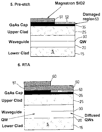
Referring now to Figures 5(a) to (g), there is illustrated a first embodiment
of a
method of manufacturing an optical device 40 from a device body portion 5,
2 5 including a Quantum Well (QW) structure 30 according to the present
invention,
the method including the steps (see Figures 5(d) to (e)) of processing the
device
body portion 5 so as to create extended defects at least in a portion 53 of
the device
body portion 5.
12
CA 02435964 2003-07-24
WO 02/061814 PCT/GB02/00445
The method of manufacture begins (see Figure 5(a) with the step of providing
substrate 10, growing on the substrate 10 first optical cladding layer 15,
core
guiding layer 20 including at least one Quantum Well (QW) 30, second optical
cladding layer 25, and cap layer 35.
The first optical cladding layer 15, core guiding layer 20, second optical
cladding
layer 25, and cap layer 35 may be grown by known semiconductor epitaxial
growth techniques such as Molecular Beam Epitaxy (MBE) or Metal Organic
Chemical Vapour Deposition (MOCVD).
Once the device of body 5 has been grown - normally as part of a wafer (not
shown) including a plurality of such device body portions 5, a dielectric
layer 51
is deposited on a surface 52 of the cap layer 35 (see Figure 5(b). A pattern
is then
defined in Photoresist (PR) 55 on a surface 54 of the dielectric layer 51. The
Photoresist 55 is then lifted off so as to leave at least one portion 56 of
the
dielectric layer 51 exposed (see Figure 5(c)).
Referring to Figure 5(d), the Photoresist 55 and at the least one portion 56
of the
dielectric layer 51 are then removed by known etching techniques, eg wet or
dry
2 o etching. In the case of wet etching Hydrofluoric (HF) acid may be
employed.
Referring to Figure 5(e), the device body portion 5 is processed so as to
create
extended defects at least in a portion 53 of the device body portion 5. The
step of
processing the device body portion 5 comprises performing a plasma etch on the
2 5 device body portion 5 using a sputterer 65 as will hereinafter be
described in
greater detail. This step may be referred to as a "pre-etch", and involves
reversing
the conventional electrical bias voltage configuration of the sputterer 65.
Refernng to Figure 5(f), a further dielectric layer 60 is then deposited on
the
13
CA 02435964 2003-07-24
WO 02/061814 PCT/GB02/00445
dielectric layer 51 and on the at least one portion 53 of the device body
portion 5.
The dielectric layer 51 and further dielectric layer 60 are deposited by use
of the
sputterer 65. In a modification the dielectric layer 51 and/or the further
dielectric
layer 60 may be deposited by a deposition technique other than by the use of a
sputterer, eg Plasma Enhanced Chemical Vapour Disposition (PECVD).
Referring briefly to Figures 6 and 7, the dielectric layer 51 is deposited by
sputtering, and in this embodiment the dielectric layer 51 is deposited by
sputtering using a magnetron sputterer apparatus, generally designated 65. The
s o dielectric layer 51 substantially comprises Silica (Si02), but may in a
modification
comprise another dielectric material such as Aluminium Oxide (A1203).
As can be seen from Figure 6, the sputterer apparatus 65 includes a chamber 70
which, in use, is substantially filled with an inert gas such as argon which
is
preferably provided within the chamber 70 at a pressure of around 2 microns of
Hg. The sputterer 65 also comprises an RF source 75 connected to a target
electrode 80 and to a substrate electrode 85 of the sputterer 65 respectively.
A
silica target 81 is provided on the target electrode 80, while the device body
portion 5 (on wafer 82) is provided on the substrate electrode 85 of the
sputterer
2 0 65. In use, an argon plasma (not shown) is generated between the target
electrode
80 and substrate electrode 85 with first and second dark spaces being provided
between the Silica target 81 and the argon plasma and between the argon plasma
and the device body portion 5, respectively.
2 5 The step of processing the device body portion 5 so as to create extended
defects
at least in a portion of the device body portion S comprises part of a Quantum
Well
Intermixing (QWI) process used in the manufacture of the device 40, the QWI
process comprising - in a preferred embodiment - an Impurity-Free Vacancy
Disordering (IFVD) technique. It has been surprisingly found that by
sputtering
14
CA 02435964 2003-07-24
WO 02/061814 PCT/GB02/00445
from the device body portion S using the sputterer 65, damage induced extended
defects appear to be introduced into the portion 53 of the device body portion
5;
the portion 53 in this case comprising part of the cap layer 35. It is
believed that
the damage in the cap layer 35 prior to annealing (which will hereinafter be
described), eg the application of thermal energy by rapid thermal annealing,
inhibits transfer of Gallium from the portion 53 of the cap layer 35 into the
further
dielectric layer 60.
The dielectric layer 51 is preferably between 10 to 1000 rim, and typically
200 nm
or 300 nm, in thickness. The method of manufacture includes a further step as
shown in Figure 5(f) of depositing a further dielectric layer 60 on the
surface 52
of device body 5 and on a surface of the dielectric layer 51 prior to
annealing. The
further dielectric layer 60 may be deposited by a technique other than
sputtering,
e.g. by Plasma Enhanced Chemical Vapour Deposition (PECVD).
The dielectric layer 51 therefore comprises an intermix cap layer, while the
further
dielectric layer 60 comprises an intermix suppressing cap layer. The intermix
suppressing cap layer is used to protect the surface 52 from Arsenic
desorption.
The method will work without the intermix suppressing cap layer; however the
2 o quality of the surface 52 may not be so good.
As shown in Figure 5(g), subsequent to deposition of the further dielectric
layer
60, the device body portion including the dielectric layer 51 and further
dielectric
layer 60 is annealed at an elevated temperature. The annealing stage comprises
a
2 5 rapid thermal annealing stage, the annealing temperature being between 700
and
1000°C, and more preferably between 800 and 1000°C, for between
0.5 to 5
minutes. In a preferred implementation, the rapid thermal anneal is
approximately
900°C for approximately 1 minute.
CA 02435964 2003-07-24
WO 02/061814 PCT/GB02/00445
The action of the annealing step of Figure 5(g) is illustrated
diagrammatically in
Figures 8(a) and (b). As can be seen from Figures 8(a) and (b), the annealing
step
causes "out diffusion" of Gallium from the cap layer 35 to the intermixing
cap, ie
dielectric layer 51. However, portions of the cap layer 35 below portion 53
and
the suppressing cap, ie further dielectric layer 60, are subject to
significantly less
Gallium "out-diffusion". The portions of the cap layer 35 which lie within an
area
of the intermixing cap, ie dielectric cap 51, are subject to greater out-
diffusion of
Gallium as shown in Figure 8(b). The out-diffusion of Gallium leaves vacancies
behind which migrate from the cap layer 35, through the second cladding layer
25,
1 o and into the core layer 20, and hence to the Quantum Well structures) 30,
thereby
changing the effective band-gap of the Quantum Well (QW) structure 30, and
effectively washing-out the Quantum Wells of the Quantum Well structure 30
below the intermixing cap layer.
1.5 It will be appreciated that the intermixing cap, ie dielectric layer 51,
is provided
within the area of the passive region 50 to be formed in device 40, while the
suppressing cap, ie further dielectric layer 60, is provided on the device
body
portion 5 in areas such as the optically active region 45 to be formed on the
device
5, which areas are not to be Quantum Well Intermixed (QWI).
Once the device body portion 5 has been processed to the stage of Figure 5(g),
and
annealed, the dielectric layer 51 and further dielectric layer 60 may be
removed by
conventional methods, eg wet or dry etching.
2 5 It will be appreciated that in the step of processing the device body
portion 5 so as
to produce extended defects at least in a portion 53 of the device body
portion 5,
any sputtering apparatus may be employed. Particularly magnetron sputterers
such
as the magnetron sputterer 65 illustrated in Figures 6 and 7 can be used.
16
CA 02435964 2003-07-24
WO 02/061814 PCT/GB02/00445
In magnetron sputterers it is attempted to trap electrons near the "target" so
as to
increase their ionising effect. This is achieved with electric and magnetic
fields
which are generally perpendicular. It will be appreciated that a number of
magnetron sputterer configurations are l~nown such as the cylindrical
magnetron
illustrated in Figure 9(a), the circular magnetron illustrated in Figure 9(b),
or the
planar magnetron illustrated in Figure 9(c). The various parts of the
magnetron
sputterer apparatus 65 a, b, c of Figures 9 a, b, c, respectively are
identified by the
same reference integers as the magnetron apparatus 65 of Figures 6 and 7.
1 o It will be appreciated that in the step of Figure 5(b) the device body
portion 5
comprises the substrate 82 of the sputtering apparatus 65 of Figures 6 and 7,
while
the silica target 81 is the target from which silica deposition occurs. This
is also
the case in the deposition stage of the further dielectric layer 60 of Figure
5(f).
However, in the step of Figure 5(e) the bias voltages are reversed, and the
wafer
82 in effect becomes the sputtering target from which sputtering occurs. This
so-
called "pre-etch" stage appears to introduce the extended defects into the
portion
53 of the device body portion 5. Between the step Figure 5(e) and Figure 5(f),
the
bias voltages are again reversed.
2 o EXAMPLE
There now follows an example which illustrates a typical band-gap sluft which
can
be obtained using IFVD in a method of manufacturing an optoelectronic device
according to the present invention in an aluminium alloy such as Aluminium
Gallium Arsenide (AIGaAs), grown on a Gallium Arsenide (GaAs) substrate.
The sputter chamber 70 is configured as follows. A plate separation of the
order
of 70 to 100 mm between the target electrode and the substrate electrode is
provided, preferably 70 mm. The electrode configuration is a 4 or 8 inch
circular
plate (preferably 8 inch). The gas used in the system is typically argon but
other
17
CA 02435964 2003-07-24
WO 02/061814 PCT/GB02/00445
gases may be used. Also a small amount of oxygen may be added to the plasma
(approximately 10% by volume) to improve the stoichiometry when performing
dielectric film deposition. The dielectric used for the process is typically
Si02, but
others such as A1203 can be used. The pressure used within the chamber 70 for
both the pre-etch and the silica deposition process is around 2 microns of Hg.
The following table outlines the resulting shifts for samples with 200 rim of
sputtered silica deposited on top of them. One sample had a 5 minute pre-etch
at
power level of 500 W. The figures in the Table detailing the shift are for an
anneal
1 o at 900°C for 1 minute.
TABLE 1
Deposition conditions Shift
Only sputtered Silica 45 nm
Sputter-etched then encapsulated with sputtered2 nm
silica
Table 1 illustrates that performing a sputter etch on the device body portion
prior
s 5 to silica (Si02) encapsulation provides an improved intermix suppressing
cap.
To process a wafer to produce more than one band gap a film of sputtered or
PECVD silica is deposited on to the wafer. Photolithography techniques are
then
used to delineate a pattern on top the sputtered silica and either wet or dry
etching
2 o can then be used to transfer the pattern into the sputtered silica.
The sample is then placed into the sputtering apparatus (rig) for pre-etching
and
a subsequent further sputtered silica deposition.
2 5 A rapid thermal anneal is now performed at a suitable temperature
(700°C -
18
CA 02435964 2003-07-24
WO 02/061814 PCT/GB02/00445
1000°C, and more preferably 800°C -1000°C) for the
required period of time (0.5
to 5 min). This enables the point defects generated at the surface in the
magnetron
silica to propagate through the structure and cause interdiffusion of the
elements.
It will be appreciated that the embodiments of the invention hereinbefore
described are given by way of example only, and are not meant to limit the
scope
thereof in any way.
It should be particularly understood that sputtered silica is suitable for
performing
1 o the IFVD process in around 980 nm GaAslAlGaAs material. Furthermore, using
a combination of a sputter pre-etch and sputtering to deposit another silica
layer,
provides an effective QWI suppression layer.
It is believed that using the pre-etch causes high levels of damage and the
occurrence of extended defects in the cap (top layer) layer of the epitaxial
wafer.
These extended defects effectively trap point defects and stop them from
diffusing
down to the QW, thus effectively stopping any intermixing of the QW. The
damage arises from the bombardment of ions at the sample surface.
2 o In the sputtering arrangement used for the process the substrate can be
switched
from being the anode / cathode of the system. Initially, the electrode on
which the
sample is located (the "substrate electrode") is made negative and the
positive ions
in the plasma are accelerated to the surface thereof causing a high degree of
damage to the cap layer, (ie the extended defects).
Further, it will be appreciated that using effectively the same type of silica
for the
whole process circumvents a problem of IFVD with dielectric caps, namely
mismatch of the expansion of coefficients thereof. This allows the post anneal
quality of the material to be kept to a high quality.
19
CA 02435964 2003-07-24
WO 02/061814 PCT/GB02/00445
It will further be appreciated that an optical device according to the present
invention may include a waveguide such as a ridge or buried heterostructure or
indeed any other suitable waveguide.
It will also be appreciated that the Quantum Well Intermixed (QWI) regions may
comprise optically active device(s).
Further, it will be appreciated that sequential processing including using
several
RF powers may be used to provide a device with several different QWI band-
gaps.
20