Note: Descriptions are shown in the official language in which they were submitted.
CA 02437000 2003-06-03
DIGITAL VIDEO SCREEN DEVICE
FIELD OF INVENTION
The present invention relates to a video screen
characterized by a display device that is entirely
digital having non-limiting applications in computer
video screens and televisions having a small thickness
and having a large, one-piece display that is planar,
cylindrical or spherical.
BACKGROUND OF THE INVENTION
Nearly all elements of today constituting the "video
chain" are digital, since the capture of an image by CCD
cell digital cameras, image processing, transmission and
reception of digital circuit televisions.
Nevertheless, in the present state of technology, video
screens belonging to the "last link", specifically video
CA 02437000 2003-06-03
displays, are not really digital. In effect, video
display devices that are type CRT, liquid display,
plasma, plasma controlled crystal liquids,
electroluminescent diodes, micro mirror modules, field
effect etc. use electronic circuits that transform
digital signals into either analog signals, or else into
frequency modulated signals allowing global variation of
the intensity emitted by red, green and blue subpixels,
grouped into triplets or pixels to form a video screen.
According to the three color additive law, the sum of the
intensity of each sub-pixel emitting the primary colors
red (R), green (G) and blue (B) light, forming a triplet
RGB referred to as pixel, results in a color that is
characteristic of the sum of luminous intensity of the
three sub-pixels. Each red, green and blue sub-pixel has
256 levels of intensity, resulting in more than 16
billion different colors per RGB pixel.
In the current state of technology, giant video screens
are implemented by assembling an array of smaller screens
that are placed side-by-side. Connected to a high-speed
electronic video, an image is decomposed into as many
elements as there are smaller screens in the mosaic. The
screens forming the mosaic can be of the CRT type, diode
panels, overhead projectors, video or liquid crystals,
micro mirrors etc. These giant screens are dozens of
inches thick and are large energy consumers. In fact,
the inherent limitations of these different types of
screens imposes the use of a screen array as soon as it
is desired to have display dimensions greater than that
of a single screen. In general, the limitations of each
of these technologies are such that for LCD screens, it
is not possible to have a video screen as a single unit
of more than 20 diagonal inches it, and for CRT and
2
CA 02437000 2003-06-03
plasma screens, it is not possible to go beyond 42
diagonal inches.
Present techniques also have limitations with respect to
image refresh rate. There exists a narrow relationship
between the refresh rate, that is, the number of times
per second that the image is reconstituted by the
display, and image resolution, that is, the number of
points per line by the number of lines per image, and the
loading rate or image change rate, that is, the number of
images displayed per second (for a film is 25 images/s in
Europe and 30 images/s in North America), and the image
dimensions. In effect, whatever the image change rate,
whether 25 or 30 images/s, the greater the resolution
and/or the dimension of the image, the less the image
refresh rate is. This is due to the way the different
display technologies work. The currently used display
technologies can be grouped into two broad categories:
scanning techniques for CRT, micro mirror and field
effect type screens, and matrix techniques for diode
type, liquid crystals and plasma screens. Commercial
television screens now attaining a refresh rate of 100 Hz
for a 42-inch diagonal dimension are near a maximum
performance level. Good quality computer screens with
display dimensions from 17 to 22 inches diagonal attain
240 Hz for a resolution of 640 points for 480 lines, but
this refresh rate decreases rapidly down to 120 Hz for
1024 x 768 resolution, to 75 Hz for 1600 x 1200
resolution.
The current techniques can only provide screens
whose surface is planar or slightly cylindrical, in the
case of multi-screen arrays, where the thickness of the
screen grows with the diagonal dimension of the display
3
CA 02437000 2003-06-03
surface. None of those techniques allow for a giant one-
piece screen where the display surface is planar,
cylindrical or spherical while remaining thin.
OBJECT OF THE INVENTION
The obj ect of the present invention is thus to provide a
new integrated circuit based display for making video
screens having five principal characteristics. First,
the video screen is entirely digital having a thickness
comparable to that of a LCD. Second, the refresh rate is
very high and independent of the resolution, the image
change rate and the display dimensions of the images.
Third, each displayed image appears all at once without
pixel scanning or requiring matrix addresses. Fourth,
the video screen always has a small thickness and a one
piece display surface, even for giant screens with
dimensions greater than 42 inches diagonal. Fifth, the
screens can provide display surface having any possible
shapes: planar, cylindrical and even spherical.
BRIEF DESCRITGION OF THE DRAWINGS
Figure 1 is a diagram of a digitally controlled basic
luminous unit.
Figure 2 is a timing diagram of the digitally controlled
basic luminous unit.
Figure 3 is a set of digitally controlled basic luminous
units connected together according to a preferred
embodiment of the present invention.
4
CA 02437000 2003-06-03
Figure 4 is an address table of the set of digitally
controlled basic luminous units connected together
according to a preferred embodiment of the present
invention.
Figures 5 and 6 are equivalent electrical circuit
diagrams and operation diagrams of the digitally
controlled basic luminous unit according to a preferred
embodiment of the present invention.
Figure 7 is a diagram of a basic luminous unit with a
digital control device.
Figure 8 is an equivalent diagram of the basic luminous
unit with the digital control device.
Figure 9 is a cross sectional view of a basic luminous
unit with a digital control device, according to a
preferred embodiment of the invention.
Figure 10 is a cross sectional view of a set of digitally
controlled basic luminous units forming a subpixel,
according to a preferred embodiment of the invention.
Figure 11 shows the relationship established between a
subpixel and a set of digitally controlled basic luminous
units according to a preferred embodiment of the present
invention.
Figure 12 is an electrical circuit diagram equivalent of
a set of digitally controlled basic luminous units and
their inputs, forming a subpixel, according to a
preferred embodiment of the present invention.
5
CA 02437000 2003-06-03
Figure 13 is an equivalent diagram of the electronic
circuit of the subpixel shown at Figure 12.
Figure 14 is an electrical connection diagram of the
subpixel shown at Figure 13, connected to a double memory
device, according to a preferred embodiment of the
present invention.
Figure 15 is an equivalent diagram of the electronic
circuit shown in Figure 13.
Figure 16 is an electrical connection diagram of a set of
three subpixels shown in Figure 16, connected to a
loading device, according to a first preferred
embodiment.
Figure 17 is an equivalent diagram of the electronic
circuit shown in Figure 16.
Figure 18 is an electrical connection diagram of a set of
n by m (n,m) subpixels, shown at Figure 17, forming an
(n, m) block of subpixels according to a first preferred
embodiment.
Figure 19 is an equivalent diagram of the electronic
circuit of the block of (n, m) subpixels shown in Figure
18.
Figure 20 is a timing diagram of the electronic circuit
forming the block of (n,m) subpixels of Figure 19.
Figure 21 is an electrical connection diagram of a set of
(n,m) blocks of subpixels, shown in Figure 19, forming a
6
CA 02437000 2003-06-03
screen of (n, m) blocks of subpixels, according to a first
preferred embodiment.
Figure 22 is an electrical connection diagram of a video
S screen formed from (n,m) blocks of subpixels, shown in
Figure 21, according to a first preferred embodiment.
Figure 23 is an electrical connection diagram of a block
of (n,m) subpixels shown in Figure 17, and forming a
block of (n, m) subpixels according to a second preferred
embodiment.
Figure 24 is an equivalent diagram of the electronic
circuit of a block of (n,m) subpixels shown in Figure 23,
according to the second preferred embodiment.
Figure 25 is an electrical connection diagram of a video
screen formed from (n,m) blocks of subpixels shown in
Figure 24, according to a second preferred embodiment.
Figure 26 is an electrical connection diagram of a set of
three subpixels shown in Figure 15, with a loading device
allowing the formation of a triplet, referred to as
pixel, according to a third preferred embodiment.
Figure 27 is an equivalent diagram of the electronic
circuit of the triplet, referred to as pixel, shown in
Figure 26, according to the third preferred embodiment.
Figure 28 is an electrical connection diagram of a block
of (n,m) pixels shown in Figure 27, according to the
third preferred embodiment.
7
CA 02437000 2003-06-03
Figure 29 is an equivalent diagram of the electronic
circuit of a block (n,m) of pixels shown in Figure 28,
according to the third preferred embodiment.
Figure 30 is a connection diagram of a video screen
formed from (n,m) blocks of pixels shown in Figure 29,
according to the third preferred embodiment.
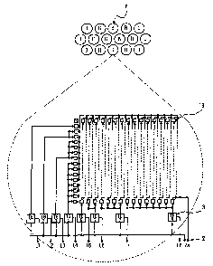
Figure 31 is a video screen with its principal elements.
DETAILED DESCRITGION OF THE INVENTION
The preferred embodiment of the present invention is
provided herein solely as an example.
The device illustrated in Figure 1 comprises a means 1,
referred to as a basic illumination cell LU, which is
directly connected to one of the terminals of a means 2,
referred to as an input source Va, and is connected to
the other terminal of the means 2 through an intermediary
of a means 3, referred to as switch SW.
Figure 2 is a diagram showing the operation of the device
in Figure 1. The input source 2 Va is constantly present
as either a continuous or periodic voltage, and is or is
not applied to terminals of the basic cell LU depending
on whether the switch SW is open or closed. Every time
the switch SW is closed for a certain amount of time, the
means 1, referred to as basic luminous unit LU, emits one
or more photon fluxes, that is, a number of photons
discharged per unit of time in a photonic unit system.
Such flux is characterized by its nature and type of
input Va applied. By selecting an input Va suitable to
the nature of the basic luminous unit LU, the behavior of
8
CA 02437000 2003-06-03
the basic luminous unit LU can be controlled in that for
a given basic amount of time Va is applied (called herein
"Te"), the same basic photon flux (called herein "~e")
will always be emitted by LU. Since the basic luminous
unit 1 emits the flux according to a corresponding solid
corresponding angle, the basic flux ~e is equivalent to a
basic luminous intensity output by the luminous unit 1.
Figure 3 is a connection diagram of a set of means 1,
referred to as basic luminous units LU, arranged in a 16
by 16 array and connected to an input source 2 Va by an
intermediary means 3, which are switches SW numbered from
1-8, according to a non-limiting example of
implementation of the present invention. The darkened
means 1, referred to as LU, represent the LUs that are
not activated by the input source Va because the switches
3 that they are connected to are open. The lighter LUs
represent those that are activated by the input source 2
Va because the switches 3 that they are connected to are
closed. The switches 3 numbered from 1-8 thus allow
application or non-application of the input source Va to
groups of LUs according to the preferred non-limiting
embodiment. In the embodiment, the switches 3 allow
grouping a number of LUs equal to the power of (n-1),
where n is the number of switches to which the LU connect
to the input source Va.
Figure 4 is an address table showing that 1-255 means 1,
referred to as basic luminous unit LU, can be activated
using only 8 address bits applied to the switches 3,
numbered 1-8. The switches allow or do not allow
application of the input source Va to the groups of LU
according to the non-limiting example of implementation.
In particular, when all switches 3 are open, the address
9
CA 02437000 2003-06-03
controls of SW are all zero (0), and all the LU are
deactivated and do not emit any photon flux, whereas when
all switches 3 are closed, the address controls are all
one (1) and all the LU are activated and emit a basic
flux ~e at the same time, resulting in a total flux asp =
255 x Vie. Each means l, referred to as LU, emits the
same basic photon flux ~e when activated. In accordance
with this non-limiting example of implementation, a
resulting flux asp capable of having 1-255 times the flux
as the basic flux ~e can be obtained. Thus, in addition
to a resulting flux asp - 0 when nothing is activated,
there are 256 possible values for the resulting flux asp:
Many kinds of LU and suitable types of input Va will
achieve this result. In a non-limiting example, the LU
are simple filament or flash lamps, electroluminescent
LED diodes and thin film electroluminescent (TFEL) or
plasma cells. Non-limiting examples of input Va are a
frequency or alternating voltage such that when the
switches SW are transistors that connect or disconnect
the lamps, diodes or TFEL or plasma cells from the input
Va, the lamps, diodes or TFEL or plasma cells will
respectively emit or do not emit the basic flux Vie. The
LU can also be liquid crystal cells, light emitting
polymer (LEP) or micro mirrors that are or are not
activated depending on whether the switches SW connect
them to the input Va such that there is a continuous
voltage.
These solutions can all be practically implemented, but
present constraints and limitations that do not give
results as satisfying as those of the now-described
device and which is a preferred, non-limiting embodiment
CA 02437000 2003-06-03
of the present invention for attaining the objectives
stated earlier.
Figure 5 is an electronic connection diagram of the
preferred embodiment, and next to it is a corresponding
specific operations diagram. A means 1, referred to as
basic luminous unit LU, is a cell containing a gas
composition having particular luminous properties when
suitably excited and ionized by a suitable input. A
means 4, referred to as capacitance C, is connected to
one of the terminals of means 1 and to one ~of the
terminals of an input source 2 Va via switch 3. The
other terminal of the input source 2 Va is directly
connected to the other terminal of the basic luminous
unit 1. In a non-limiting example, the input source 2 Va
generates an alternating voltage represented on the
diagram by a sinusoidal curve VOLTAGE Va. The dotted
VOLTAGE PT A curve shows in a simplified manner,
variations of the voltage measured at a point A in the
connection diagram. The connection diagram illustrates
two modes of operation, depending on whether the switch 3
is open or closed, which is represented by the curve
STATE OF SW. In the first mode, if switch 3 is open, no
input voltage Va is applied to the device and nothing
happens since the basic unit 1 is not connected to the
input source 2 Va, which is thus deactivated or unlit.
In the second mode, switch 3 is closed and the input
voltage Va is thus applied to the whole circuit. The
VOLTAGE PT A curve shows that the voltage measured at
point A remains at a constant value until the absolute
value of the input voltage IVaI reaches a value IVi~,
referred to as an ionization voltage. The ionization
voltage I Vi I is precise and specific to a gas, that when
ionized, becomes luminous. When the absolute value of
11
CA 02437000 2003-06-03
the input voltage IVaI is less than the ionization
voltage ~Vil, internal resistance of the gas contained in
the basic cell LU is so high that the internal resistance
can be considered infinite. No current passes through
the gas that is not ionized and the gas does not emit
luminescence. From the moment that the input voltage
IVaI reaches the ionization voltage IViI, the gas
contained in the basic elementary unit LU cell ionizes
and becomes luminous whereas the internal resistance
diminishes sharply. The current passing through the
luminous ionized gas is sufficient to charge the
capacitance 4 such that the voltage at point A raises
toward the input voltage Va until reaching a value of
~IVi + ovl (~ depends on current direction) is reached.
By tracking the input voltage Va, the absolute value of
the difference between the potential applied to the
terminals of the basic cell 1 goes below the absolute
value of the ionization voltage IViI and the ionization
of the gas and its accompanying luminescence stops. The
current no longer passes through and the voltage measured
at point A is maintained at the value ~IVi + w 1. The
STATE OF LU curve in the diagram shows that for a period
of the input voltage Va, when peak-to-peak amplitude is
slightly more than 2 times the absolute value of the
ionization voltage IViI, four luminous ionizations of the
gas for basic cell 1 are obtained when switch 3 is
closed. If the input voltage Va has a peak-to-peak
voltage slightly more than one times the absolute value
of the ionization voltage IViI, 2 luminous ionizations
per period are obtained, whereas if the input voltage Va
has a peak-to-peak amplitude slightly more than 4 times
the absolute value of the ionization voltage IViI 8
luminous ionizations per period are obtained, etc. In
the preferred embodiment, the ionization time Ti of the
12
CA 02437000 2003-06-03
gas and therefore of the luminescence of the basic cell
l, is essentially a function of the resistance of the
input source, the nature and pressure of the gas and the
value of the capacitance C. However, no matter the value
of these parameters, the ionization time Ti of the gas is
globally always the same in this type of function, which
makes the basic cell LU emit by luminescence basic photon
flux ~e having globally identical values with each
ionization of gas during the basic time Te=Ti.
Figure 6 shows the same arrangement as Figure 5 except
the switch SW has been replaced by a digitally controlled
electronic transfer gate TG, which in a non-limiting
example is comprised of transistors, such that the
circuit may or may not be in communication with the input
source 2 Va, depending on whether a logical input L is
one (1) or zero (0) which is represented by curve
STATE OF L in the diagram. Hence, the diagram shows the
operation of the device over several periods and shows
the input voltage Va, the voltage measured at point A and
the luminous ionization impulse curve STATE OF LU.
Several conclusions can be drawn from the diagram.
First, if the frequency of the input voltage is raised,
the function of the device does not change, only the
interval between each ionization impulse is reduced which
means an increase in their frequency, hence in the
luminous impulses of the basic flux Vie. Likewise, if the
peak-to-peak value of the input voltage is increased such
that the value is slightly greater than a multiple of the
ionization voltage Vi, the number of ionizations per
period is multiplied which also decreases the interval
between them, hence increasing the rate of luminous
impulses Vie. Of course, the two cases can be combined by
increasing both the rate and the peak-to-peak amplitude
13
CA 02437000 2003-06-03
of the input voltage to increase the rate of luminous
impulses cue. In all cases, since the slope of the input
voltage increases, the ionization time Ti and hence the
duration of the luminous impulses of basic flux ~e
decrease, though globally they will always have the same
value. In the preferred non-limiting embodiment,
globally identical luminous impulse rates ~e of several
kHz or even MHz can be obtained, each of the luminous
impulses cDe being the result of an ionization of duration
Ti during which a basic flux ~e is emitted over basic
time Te=Ti. Thus, the transfer gate serves as a simple
digital binary control allowing luminous impulses
emitting basic photon flux Vie. Since the rate of
luminous impulses cue can be very high, the rate of the
digital control transfer gate can also be high, easily
25-30 Hz, if not greater.
Figure 7 is a diagram of a basic luminous unit 1
connected to one of the terminals of the input source 2
Va and connected to a capacitance 4. The capacitance 4
is connected to a transfer gate 3, which is connected to
the other terminal of input source 2 Va. The transfer
gate 3 is set by a digital control input L accepting two
logic states, zero (0) and one (1).
Figure 8 is an equivalent diagram of the electronic
circuit of Figure 7. A circuit 5 comprises the set of
luminous unit 1, the capacitance 4 and the transfer gate
3. The circuit can be connected to an input source 2 Va
and an input L receives a binary logic control.
Figure 9 is a physical cross sectional view of a
preferred embodiment for a basic luminous unit with a
digital control device. An interior face of a
14
CA 02437000 2003-06-03
transparent support 6 receives a layer of luminescent
substance 7 and a transparent electrode 8. At a suitable
distance is an insulating support 9. On one of the faces
of insulating support 9 is placed electrodes 10 and 11,
which are separated by a dielectric 12. The set of means
10-12 forms a capacitor 4, which is surrounded by an
insulator 13. The electrode 8 is implemented using a
uniform conducting substance transparent to photon flux,
or in form of a fine conducting grid that is directly
connected to one of the terminals of the input source 2
Va. The electrode 11 is connected to a transfer gate 3,
which is connected to the other terminal of the input
source 2 Va. The transfer gate 3 blocks or conducts
depending on the application of a logical signal zero (0)
or one (1) to an input L. Inverse logic can also be
applied. Between the two sets of means 6-8 and 10-12 is
a gas 14 having a composition and pressure similar to
those used, in a non-limiting example, in plasma screens
that when suitably excited and ionized emit by
luminescence a flux of photons 15 having a wavelength
characteristic of their composition and pressure. When
the transfer gate 3 is blocked, for example from the
application of a 0 at the input L, nothing happens since
no voltage outputs from the input source 2 Va to apply to
the device. When the transfer gate 3 conducts, for
example from the application of a 1 at the input L, there
is a series of ionization impulses of gas 14 that
generate a corresponding series of luminous impulses 15
and therefore a basic photon flux ~e having a particular
wavelength. The basic photon flux ~e having a particular
wavelength traverses the electrode 8 and is transformed
by the luminescent substance 7. The luminescent
substance 7 emits by luminescence a basic photon flux Vie,
represented by arrows 16, having a wavelength
CA 02437000 2003-06-03
characteristic of its composition and which passes
through the transparent support 6 which can be glass or
polycarbonate. In a non-limiting example, the
compositions of the luminescent substances 7 can be
similar to those used in plasma screens, and depending on
its composition, emits photon flux corresponding to
primary colors of red, green and blue light, or a mixture
of these colors to obtain white or any other specific
color. In contrast to existing plasma devices, the
activation voltage is much weaker, in the order of volts
or dozens of volts, since it relates to the ionization
voltage IViI. Furthermore, there is no need for
supplementary electrodes for the voltage maintaining
discharges, nor a device for discharge currents control
since the arrangement uses high frequency basic luminous
ionization impulses ~e where discharge currents are self-
limited by the capacitance 4. The capacitance 4 is a few
nano or dozens of nano farads depending on the
conductance of the ionized gas and the ionization time
value Ti that is desirably obtained as basic time Te for
the basic flux Vie. The device therefore consumes very
little current, on the order of micro amps, because it
concerns ionization of plasma which will always work in a
subnormal and normal luminous mode of discharge without
ever entering a luminous arc mode that is a great
consumer of current and that causes energy dissipation by
heating the plasma.
Figure 10 is a cross sectional view of a preferred
embodiment of a set of identical, digitally controlled
basic luminous units LU similar to the one in Figure 9,
forming a subpixel. The basic units LU are arranged in a
16 by 16 array connected according to the preferred
arrangement shown in Figure 3, to transfer gates numbered
16
CA 02437000 2003-06-03
TG1-TG8. A means 17 delimits the set. A support 6
covers the set and itself is covered by a common layer of
substance 7 and by a common electrode 8 which is shared
by the set of luminous units and directly connected to
the input source 2 Va. Figure 10 shows, for example,
that when a logic control (1) is applied to the input L
of one or more transfer gates 3, luminous gas ionization
impulses 15 are enabled, whereas they are disabled when a
logical zero (0) control is applied to the input L of one
or more transfer gates 3. A binary word of n=8 bits
allows 2n, or 256 values, of total photon flux emitted by
identical impulses asp - 2° x ~e by the luminescent
substance 7 at a rate that is a function of the input
source 2 Va, in accordance with what was previously
explained for Figure 6. Each basic luminous unit LU that
composes the device can and should function
independently. The capacitances 4 of each LU are
separated by an insulator 13 in order to avoid charge
transfer phenomena between neighboring active luminous
units, which would modify the function and duration Te=Ti
of each ionized basic luminous impulse Vie. The cross
sectional view shows a non-limiting example of a set
forming a red, green or blue subpixel, depending on the
emission corresponding to the composition of the
luminescent substance 7, either a red, green or blue
wavelength in response to the photon flux 15 emitted by
luminescence of the gas 14 for each of the LUs that are
activated by their transfer gate 3.
Figure 11 shows the relationship between each subpixel 18
of the RGB matrix of a video screen and a set of
digitally controlled basic luminous units LU, in
accordance with a preferred embodiment of the present
invention. Each sub pixel 18 is decomposed; according to
17
CA 02437000 2003-06-03
the preferred embodiment, into an array of 16 by 16 means
19, each means comprising a basic luminous unit LU 1 and
a capacitor. The means 19 are directly connected,
according to the preferred embodiment, to an input source
2 Va and to a transfer gate 3, numbered TGl-TG8, with
digital controls L1-L8 at the input. The dimensions of
the basic luminous units 19 are such that the dimensions
of the set correspond to a desired dimension for a
corresponding subpixel. Using a binary word of n=8 bits
applied to the digital controls of the transfer gates 3,
an activation of 1-255 basic luminous units in accordance
with Figure 4 can be obtained. A total flux of Q~sp = 2n x
~e emitted by impulses for each subpixel having 1-256
values is obtained since the deactivation of all LU of a
subpixel, corresponding to total blackness, counts as one
value. The number of basic luminous units can also be
increased or decreased to obtain a total flux asp - 2n x
~e having more or less values. For example, a binary
word having a corresponding number of bits n can be used
to implement video screens requiring more or less colors,
or bi-color screens referred to as monochromes, or half
tones used for alphanumeric information displays and/or
graphics.
Figure 12 is an equivalent electronic diagram of a set of
digitally controlled basic luminous units and their
inputs, forming a subpixel in accordance with the
preferred embodiment described in Figure 3. Each of the
luminous units 1 is directly connected to a common
terminal of input source 2 Va and to a capacitance 4.
The capacitance 4 is connected to a transfer gate 3, in
accordance with the preferred embodiment of Figures 3 and
11, and is connected to the other terminal of input
source 2 Va depending on whether the digital control
1$
CA 02437000 2003-06-03
inputs L1-L8 of the transfer gates 3 receives a
corresponding logic value.
Figure 13 is an equivalent diagram of the electronic
circuit of a subpixel. A circuit 20 is a set of elements
described in Figure 12, with inputs connected to an input
source 2 Va and to digital control inputs L1-L8 of
transfer gates 3. The function of the electronic circuit
is simple since it suffices to apply a suitable input
source Va, as described in Figures 5 and 6, to obtain a
subpixel whose set of basic impulses of photon flux
emitted by luminescence would have a value of asp - 2" x
Vie, which is determined by the value of an n=8 bit binary
word applied to inputs L1-L8. It has already been noted
that the impulse rate of flux asp is independent of the
rate at which the value of the n=8 bit binary word that
is applied to inputs Ll-L8 changes.
Figure 14 is a connection diagram of the subpixel, shown
in Figure l3, associated with a double memory device in
accordance with a preferred embodiment of the invention.
A circuit 21 symbolizes all elements described by Figure
12 with connections to input source 2 Va and to digital
control inputs L1-L8. Each input L1-L8 is connected to
the outputs of single bit memory flip-flops such that the
set constitutes an 8-bit display memory 22 having a
common digital control M. DIS. The inputs of the display
memory 22 are connected to the outputs of the single bit
memory flip-flops where the set constitutes an 8-bit next
display memory 23 having a digital control loading signal
M.NXT. The 8-bit word sent to the subpixel is sent to
inputs D1-D8 of the next display memory 23. The function
of this arrangement allows storing two different 8-bit
words depending on the application of the loading control
19
CA 02437000 2003-06-03
on M.DIS or M.NXT. The 8-bit word stored in the next
display memory 23 by the loading control M.NXT
corresponds to a binary impulse value of the next total
flux asp of the subpixel. The 8-bit word stored in the
display memory 22 corresponds to the binary impulse value
of the total flux asp that is actually emitted or
displayed by the subpixel. When the loading control is
applied on M.DIS, the 8-bit word stored in the next
display memory 23 is transferred to the display memory
22. While the subpixel emits impulses of total flux asp
determined by the value of the 8-bit word stored in the
display memory 22, it is possible to load another 8-bit
word in the next display memory 23 corresponding to the
values of impulses of the total flux asp that will be
emitted by the following subpixel. Thus, the refresh
rate of the value displayed by the subpixel is separated
from the loading rate, or rate of change of the displayed
value. For an 8-bit binary word stored in the display
memory 22 and corresponding to the value of total flux
asp emitted by the impulses of the subpixel, the impulse
rate corresponds to refresh rate of the subpixel, which
depends only on the characteristic voltage applied by the
input source 2 Va, and can be several kHz or MHz
depending on what was explained for Figures 5 and 6. The
rate of change of an 8-bit word stored in the display
memory 22 and which hence corresponds to the value of
total flux asp emitted by impulses of the subpixel,
uniquely depends on the rate at which the 8-bit binary
word stored in the next display memory 23 is changed or
is loaded into the display memory 22, and is thus
completely independent of the refresh rate of the
subpixel.
CA 02437000 2003-06-03
Figure 15 is an equivalent diagram of the electronic
circuit described in Figure 14. A circuit 24 corresponds
to a set of means, described by Figure 14, with inputs
allowing connection to an input source 2 Va, digital
input controls D1-D8 for receiving words of n=8 bits
corresponding to values of total flux asp emitted by
impulses of the subpixels, as well as a loading input
M.NXT for storage in the next display memory and a
loading input M.DIS for storage in display memory 22.
From the basic electronic circuits of Figure 13 or 15, a
video screen with a matrix of subpixels can be
implemented where the matrix of subpixels are loaded
subpixel by subpixel by a classic X,Y matrix addressing
device, such as those used for diode matrices, LCD or
plasma cells. However, this addressing method is less
interesting because it requires decoding integrated
circuits external to the display screen device, whereas
none is needed with the preferred methods of addressing
that will now be described, implemented in a manner
internal. to the device using integrated circuits and
which is the object of the present invention.
Figure 16 is an electronic connection diagram of a set of
three subpixels, as in Figure 15, associated with a
loading device in accordance with a first preferred
embodiment. The equivalent circuit described in Figure
15 is found in the three circuits 24 with inputs
connected to the input source 2 Va and inputs D1-D8
connected to a common data bus. The loading input of the
display memories 22 for the three circuits 24 are
connected together such that a loading signal M.DIS can
be sent at the same time. To identify the subpixel
concerned by the data on the bus D1-D8, three means 25
21
CA 02437000 2003-06-03
are used. The three means 25 are D flip-flops (DFF)
connected in series like in a shift register. The inputs
CP of the DFF are connected to a common clock source C
whereas the inputs R are connected to a common Reset.
Input D of the first DFF (from the left) is connected to
an input SP.PCD, where input D originates from a
preceding subpixel, if one exists, otherwise input D will
originate from an electronic control circuit. An output
Q of the first DFF is connected to both an input M.NXT of
a first circuit 24 for input loading of a next display
memory 23 and to an input D of a second DFF. The second
DFF and the third DFF are connected according to the same
principles for loading each input to the next display
memory 23 of the next two corresponding circuits 24 using
the output Q. The output Q of the third DFF is also
connected to an output SP.NXT and allows for a connection
to the input SP. PCD, hence to the input D of the loading
DFF of the next subpixel, if it exists. An example will
better illustrate the operation of the set for loading
data corresponding to each red, green and blue subpixel
forming a RGB pixel. Suppose Figure 16 is a first group
of three subpixels forming a RGB pixel. At
initialization, a Reset signal is applied. For example,
a zero (0) resets all the DFF 25 to zero. The input
M.DIS of the three circuits 24 is also zero, clearing the
display memories 22 and preventing any modification of
their contents. All the outputs Q of the DFF 25 are
zero, and consequently the input M.NXT of all the red,
green and blue subpixels do not permit loading of the
input into the next display memory 23. At a first clock
edge C (applied to all the inputs CP of the DFF 25), a
first 8-bit word is sent on the bus to the inputs D1-D8
and a single loading impulse of logical one (1) is sent
to the input SP.PCD which is connected to input D of the
22
CA 02437000 2003-06-03
first DFF. The first 8-bit word corresponds to the value
of the next total flux asp that will be emitted by the
red subpixel. The loading impulse applied to D appears
at the output Q of the first DFF and affects the input
M.NXT of the next display memory 23 of the first circuit
24 corresponding to the red subpixel by permitting the
loading of the first 8-bit word destined for the next
display memory 23. Since the other outputs Q of the
other two DFF are still zero, the other outputs Q do not
permit loading the inputs M.NXT of the other two circuits
24 corresponding to the green subpixel and the blue
subpixel respectively, and hence prevents storage of data
currently on the bus into the next display memory 23. At
a second clock edge, the 8-bit word corresponding to the
value of the next total flux asp emitted by the green
subpixel is sent on the bus. The loading impulse present
at the output Q of the first DFF and which is applied to
the input D of the second DFF and which corresponds to
the green subpixel, appears at the output Q and permits
loading the input M.NXT of the next display memory 23 for
the green subpixel. This permits placement of the 8-bit
word destined for the next display memory 23. Since the
output Q of the first DFF corresponding to the red
subpixel has returned to zero and the output Q of the
third DFF corresponding to the blue subpixel remains
zero, their inputs M.NXT do not permit loading their next
display memories . At a third clock edge, the 8-bit word
on the bus corresponding to the value of the next total
flux asp emitted by the blue subpixel is stored in the
same manner. The loading impulse is present and
available at the output Q of the third DFF, and hence at
the output SP.NXT for the next subpixels. During the
loading of data corresponding to each subpixel into the
next display memory 23, the input M.DIS of circuits 24
23
CA 02437000 2003-06-03
remains zero, not permitting loading the display memories
22. Whatever the 8-bit word stored in the display
memories 22, at initialization this word can be all ones
for example, this contents have not been modified by the
loading of the next display memories 23 and all the RGB
subpixels have emitted values of total luminous flux cusp
corresponding to the contents in the display memories 22
at a rate corresponding to their basic impulses.
Figure 17 is an equivalent diagram of an electronic
circuit of a single subpixel with a loading device. A
circuit 26 represents a single circuit 24 with a single
DFF 25, in accordance with Figure 16, with inputs
connected to the input source 2 Va, inputs D1-D8
connected to the data bus, an output SP.NXT coming from
the output Q of the DFF 25 and for transmitting the
loading signal for the next display memory 23 to the next
subpixel, an input SP.PCD for receiving the loading
signal for the next display memory 23 coming from the
output Q of DFF 25 of the preceding subpixel, an input
M.DIS for receiving the loading signal from the display
memory 22, an input for receiving the Reset signal at an
input R of the DFF 25, and an input for receiving the
clock signal C at the input CP of the DFF 25.
The electronic circuit will therefore be capable of
serving as a base for implementing a chain of subpixels
in order to form a complete video screen. The digital
circuit is simple so an integrated circuit comprising a
block of many subpixels can be achieved.
Figure 18 is an electronic connection diagram of a set of
n by m (n,m) subpixels for forming a circuit block of
(n, m) subpixels in accordance with a first preferred
24
CA 02437000 2003-06-03
embodiment. In the circuit block there are the inputs of
means 26, as described in Figure 17, which are connected
to the input source 2 Va, the inputs D1-D8 are connected
to the data bus, the outputs SP.NXT transmit the loading
signal for the next display memories 23 to the next
subpixels, the inputs SP.PCD receive the loading signal
for the next display memories 23 coming from the
preceding subpixel, the input M.DIS simultaneously
receives the loading signal for the set of display
memories 22 of the set of subpixels, the input Reset
permits simultaneous reset of the set of DFF 25 for all
the circuits 26 to zero, and the input C simultaneous
applies the clock signal C to the set of subpixels (n, m),
connected in accordance to the first preferred
IS embodiment. The operation is the same as described in
Figure 16 except there are more subpixels.
Figure 19 is an equivalent diagram for the electronic
circuit of the block of (n,m) subpixels with a circuit 27
formed from the set of elements shown in Figure 18. The
inputs are connected to the input source 2 Va, the inputs
D1-D8 are connected to the data bus, the outputs SP.NXT
transmit the loading signal for the next display memory
23 to the subpixels for the next block of (n, m)
subpixels, the inputs SP.PCD receive the loading signal
for the next display memory 23 which comes from the
preceding block of (n, m) subpixels, the input M.DIS
simultaneously receives the loading signal for the set of
display memories 22 for the set of subpixels of the
block, the input Reset simultaneously resets the set of
DFF 25 to zero for all the circuits 26 of the block, and
the input C simultaneous applies the clock signal C to
the set of DFF 25 to the block of (n, m) subpixels
CA 02437000 2003-06-03
connected in accordance to the first preferred
embodiment.
Figure 20 is a timing diagram of the electronic circuit
forming the block of (n,m) subpixels, as in Figure 19.
Shown, are pulse trains for the clock C, Reset, M.DIS,
Data RVB, SP.PCD numbered from (1,1) to (n,m), and the
graph representing the loading of each subpixel S-Pixel
(n, m). From the beginning of Reset, which can correspond
to the loading Signal M.DIS for the set of display
memories 22, the diagram shows that at each clock edge C
the data bus has an 8-bit word corresponding to the next
value of the R, G or B subpixel, whereas the loading
signal at the output of the preceding subpixel SP.PCD
(n, m) permits loading of the sub pixel S-Pixel (n, m)
having the same indices. The loading rate of the next
display memories 23 is thus a function of the clock C
rate which synchronizes the stream of data on the DATA
RGB bus applied to the inputs D1-D8 of Figure 19.
Figure 21 is an electronic wire diagram of the set of
(K, P) circuits blocks of (n, m) subpixels composed from
the circuits 27 described by Figure 18 and forming a
screen of (K, P) blocks of (n, m) subpixels, in accordance
with a first preferred embodiment. The circuits 27 of
(n,m) subpixels are connected to the same input source 2
Va and to the inputs Dl-D8 connected to a common data
bus. The loading inputs M.DIS of the display memories 22
are connected together. Likewise, are the inputs for the
clock C and Reset. When the preceding block has filled
all its next display memories with the data destined to
them, the loading signal M.NXT appears at the output
SP.NXT to load the first subpixel at the input SP.PCD of
the next circuit block of (n,m) subpixels. When all the
26
CA 02437000 2003-06-03
circuits 27 have filled their next display memories 23,
the set of values for all the subpixels corresponding the
next image becomes available in the set of next display
memories 23. At this moment, the loading signal for the
next image is sent to the input M.DIS that simultaneously
permits the transfer of contents of all the next display
memories 23 of all circuits 27 into the display memories
22. A new image appears at once in its entirety, like an
image from a motion picture film projector. In this
manner, the displayed image is refreshed in its entirety
at a rate of the luminous impulses 16 determined by the
input source Va, at several kilo or mega Hertz, such that
the image is loaded or changed at a loading signal rate
M.DIS of the display memories 22 of 25-30 images/s or 25-
30 Hertz. The objective to separate the image refresh
rate from the image loading or change rate has been
achieved. The clock C rate of the device that loads the
data corresponding to the value of each subpixel is a
direct function of the number of subpixels, hence the
resolution of the image. For example, for an image
resolution of 640 x 480 pixels, the clock rate would be
equal to 640 x 480 x 3 subpixels x 25 images/s - 23.04
MHz in Europe, and 640 x 480 x 3 subpixels x 30 images/s
- 27.648 MHz in North America. For high resolution
images, for example 1600 x 1200, the clock rate is 1600 x
1200 x 3 x 25 - 144 MHz in Europe and 1600 x 1200 x 3 x
- 172.8 MHz in North America, which are not difficult
rates to achieve for video circuits that are entirely
digital.
Figure 22 is an electronic connection diagram of a video
screen formed of (K, P) blocks of subpixels, as in Figure
21, according to the first preferred embodiment. Shown,
are blocks of subpixels 27 numbered from (1,1) to (K, P)
27
CA 02437000 2003-06-03
arranged on a support 28 which is a printed circuit
substrate on which there are paths connecting the (K, P)
blocks of (n,m) subpixels to the input source 2 Va, the
inputs D1-D8 to the data bus, the outputs SP.NXT for
loading the next display memories 23 of the next block of
subpixels, the inputs SP.PCD for loading the next display
memories 23 coming from the preceding block of subpixels,
the respective corresponding inputs for the simultaneous
loading signal M.DIS of all display memories, the clock
signal C and the Reset signal. All the information is
available on the printed circuit substrate and allows
connection to many like screens for forming a larger
screen without it being necessary to use external video
circuits. The preferred embodiment of the video screen
achieves three of the five characteristics identified as
the objective. First, it is an entirely digital display
device that has a small thickness since it is formed of
an array of (K,P) integrated circuits 27. Second, the
refresh rate is very high and independent from the
resolution, the rate of change, and the image display
dimension since it is uniquely the function of the input
voltage Va which causes the luminous impulses of total
basic flux cDsp. Third, each displayed image appears at
once, without any pixel scanning or matrix addressing
since all the circuits 27 are connected to a common data
bus and it is the simultaneous loading signal M.DIS of
the display memories 22 that transfers all at once the
contents of the set of next display memories 23 to the
set of display memories 22, such that the image appears
globally like the image from a motion picture film
projector.
Two other preferred embodiments will now be described for
a video screen having the same characteristics, but
28
CA 02437000 2003-06-03
concerned more specifically with the connection of the
subpixels to the next display memory 23 and the display
memory 22 for forming circuit blocks of subpixels or
pixels and finally, a video screen.
Figure 23 shows an electronic connection diagram of a
block of (n,m) subpixels, as in Figure 17, forming a
block of (n, m) subpixels in accordance to a second
preferred embodiment. The interconnection of subpixels
and their operation are identical to what was described
in Figure 18, except that this wiring achieves a grouping
of (m) lines of (n) circuits of subpixels 26. Thus,
there are (m) inputs SP.PCD with index (n, 1 to m) for
loading a line (m) of circuits 26 for a current block,
and (m) outputs SP.NXT with index (1, 1 to m) for loading
a first pixel for each of the lines (m) for a next block.
Figure 24 is an equivalent diagram of an electronic
circuit of a block of (n, m) subpixels in accordance with
the second preferred embodiment. A circuit 29 made from
the circuits described in Figure 23 has inputs connected
to the input source 2 Va, inputs Dl-D8 connected to the
data bus, outputs SP.NXT indexed (n, 1 to m) for
transmitting a loading signal of the last subpixels (n)
of (m) lines for the current block to the next block of
pixels, inputs SP.PCD indexed from (n, 1 to m) for
receiving loading signals coming from the last subpixels
(n, 1 to m) from the preceding block of subpixels, input
for receiving the simultaneous loading signal M.DIS for
the set of display memories 22 of circuit 29, input for
receiving the simultaneous Reset signal for the set of
DFF 25 for circuit 29, and input for receiving the clock
signal C simultaneously applied to the set of DFF 25 of
29
CA 02437000 2003-06-03
circuit 29 in accordance with the second preferred
embodiment.
Figure 25 is an electronic connection diagram of a video
screen formed from (K,P) blocks of (n,m) subpixels in
accordance with the second preferred embodiment. There
are (P) lines of (K) circuits 29 that are arranged on a
support 30 which is a printed circuit substrate of
interconnections for connecting the blocks of subpixels
in the manner described by Figure 22, except that for
each line (m) of each line (P) of circuit 29, loading
inputs M.PCD (1) for the first next display memories 23
of each line (m) of each block (K) of subpixels are
connected to the last loading outputs M.NXT (n) of the
next display memories 23 for the same line (m) of the
preceding block (K-1). The last loading output (n) of
the next display memory 23 for the line (m) of block (K)
is connected to the loading input (2) of the first next
display memory 23 for the line (1) of block (1, P+1). In
this manner, the data is loaded line by line for the set
of circuits 29 situated on the same line (P) and
propagates line by line (m) for blocks (P). The second
embodiment for assembly allows for a data stream on the
bus arriving at inputs D1-D8 corresponding to each
subpixel, and which is directly compatible with the data
stream issued from a line scanning and frame digital
video source, since all the same lines (m) for the lines
for the (K) blocks are filled one after another, to fill
the screen line by line. In the wire assembly described
in the first embodiment of Figures 21 and 22, the data
stream is modified since each block of subpixels must be
filled before filling the next one. In this case also,
many similar screens can be connected to form an array
without using external video circuits also, because all
CA 02437000 2003-06-03
the signals are available on the printed circuit
substrate 30.
Figure 26 is an electronic connection diagram of a set of
three subpixels, as in Figure 15, with a loading device
for forming a triplet, referred to as pixel, in
accordance with a third preferred embodiment. The same
assembly as for Figure 16 is present, with the same
inputs and outputs except that there is only one means 25
for simultaneously loading the three circuits 24 forming
a red, green and blue triplet, or RGB pixel, that. the
data bus sends 24-bit words to the inputs Dl-D8 (in a
non-limiting example, the 24-bit words are distributed to
each subpixel as 1-8 for blue, 9-16 for green, and 17-24
for red), that the loading input M.NXT of the next
display memories 23 for the three circuits 24 are
connected to the output Q of DFF 25 and the output Q
permits loading the next display memories 23 for the next
pixel using output P.NXT, and that the input D of DFF 25
is connected to the input P.PCD which receives the
loading signal coming from the output Q of DFF 25 of the
preceding pixel.
Figure 27 is an equivalent diagram of the electronic
circuit of a triplet, referred to as RGB pixel, in
accordance with the third preferred embodiment. The
means 31 is shown in Figure 26. The connections are the
same as in Figure 17, except there are 24 inputs D1-D24,
an input P.PCD (instead of SP.PCD), and an output P.NXT
(instead of SP.NXT).
Figure 28 is an electronic connection diagram of a block
of (n, m) pixels 31, as in Figure 27, in accordance with
the third preferred embodiment. The connections and the
31
CA 02437000 2003-06-03
operation are similar to what is described in connection
with Figure 23. That is, a grouping of (m) lines for (n)
circuits 31, except that the data bus is now 24 bits
connected to inputs D1-D24, that the loading inputs of
the next display memories 23 for the preceding pixels are
P.PCD (n, 1 to m), and that the loading outputs of the
pixels for the next blocks are P.NXT (n, 1 to m).
Figure 29 is an equivalent diagram of the electronic
circuit of the block of (n,m) pixels in accordance with a
third preferred embodiment. The circuit 32 described by
Figure 28 is connected in a manner identical to Figure
24, except that the data bus is now 24 bits connected to
inputs D1-D24, that the loading inputs of the next
display memories 23 for the preceding pixels are P.PCD
(n, 1 to m), and that the loading outputs of the pixels
for the next blocks are P.NXT (n, 1 to m).
Figure 30 is a connection diagram of a video screen made
up of (n,m) blocks of pixels, as in Figure 29, in
accordance with the third preferred embodiment. The
wiring and operation are the same as described by Figure
25, except that the printed circuit substrate 33 of
interconnections on which the (K,P) circuits 32 are
connected transport a data bus of 24 bits connected to
inputs Dl-D24. The advantage of a data bus assembly of
24 bits is to allow a reduction in the loading rate of
the data into the next display memories 23 of the
subpixels, since the data does not arrive one 8-bit word
after another for red, green and blue, but arrives in
parallel at the same time on 24 bits. For example, for a
resolution of 640 x 480, the clock rate is equal to 640 x
pixels x 25 images/s - 7.68 MHz in Europe and 640 x
480 x 30 images/s = 9.216 MHz in North America. For high
32
CA 02437000 2003-06-03
resolution images, for example 1600 x 1200, the clock
rate is 1600 x 1200 pixels x 25 images/s - 48 MHz in
Europe and 1600 x 1200 pixels x 30 images/s - 57.6 MHz in
North America, which are not difficult frequencies to
attain for entirely digital video circuits.
Three out of five characteristics identified as
objectives are achieved by the screens. First, the
invention provides a display device that is entirely
digital having a reduced thickness, similar to an LCD
screen. Second, the refresh rate is high and independent
of the resolution, the image change rate and the display
dimensions of the images. Third, each displayed image
appears at once, without pixel scanning or matrix
addressing.
Figure 31 is a video screen showing its principal
constituents. Each integrated circuit 27, 28 or 32, in
accordance with one of the three non-limiting preferred
embodiments, is sealed by the electrode 8 which allows
the photon flux 15 emitted by luminescence of the ionized
gas 14 found in between, to pass through. The electrode
is common to the set of luminous units LU of the
integrated circuit since it is directly connected to the
input source 2 Va. The set 27, 29 or 32 and 8 each form
integrated circuits 34, which are wired to form an array
on a printed circuit substrate 28, 30 or 33, implemented
according to one of the three preferred embodiments
indicated, and have paths for the source Va, for the 8 or
24-bit data bus, for the clock C and for Reset, for
loading M.DIS of the display memories 22 and for loading
M.NXT of the next display memories 23. To obtain colors,
a transparent support C is placed on top of the array of
integrated circuits 34. A matrix composed of three
33
CA 02437000 2003-06-03
substances 7 is deposited on the inside face of the
transparent support 6. Depending on their composition,
the three substances emit by luminescence 16 a red, green
or blue color when the substances are excited by the
impulses of photon flux 15 emitted by the integrated
circuits 34. In a non-limiting example, the support 6 is
made by screen printing that is overlaid, subpixel to
subpixel, onto the integrated circuits 34, hence forming
a one-piece, uniform display surface even if there are
many printed circuit substrates 28, 30 or 33 underneath.
In this manner, the fourth objective is achieved, which
is to provide a video screen of reduced thickness and a
one-piece display surface with dimensions above 42 inches
diagonal, referred to as a giant screen.
With this type of integrated circuit, cylindrical screens
can be implemented because the integrated circuits 34 can
be connected to flexible printed circuit substrates, and
the support 6 that goes on top can also be flexible.
Since the integrated circuits 34 can have a hexagonal
shape, it is possible to connect these to a printed
circuit substrate of the same shape and thus obtain
spherical screens.
The objectives concerning the five principal
characteristics of the digital video screen device
implemented in the form of an integrated circuit, being
object of the present invention, are thus achieved.
Thus, the digital video screen device comprises one or
more printed circuit substrates on which are mounted one
or more integrated circuits covered by a one-piece
display surface which is covered by one or more
34
CA 02437000 2003-06-03
luminescent substances that are excited by the integrated
circuits placed underneath, such that:
a) for each subpixel 18 belonging to an image point
displayed by the video screen, there is a certain
number of corresponding basic luminous units 1 which
each emit a basic photon flux ~e corresponding to an
intensity of basic colors, when activated,
b) the basic luminous units 1 forming each subpixel 18
are all connected on the one hand, to a common
terminal of a suitable input source 2 Va, on the
other hand are activated or deactivated by the
intermediary of electronic switches 3 that,
respectively connect or disconnect one or more basic
luminous units 1 at the same time to another
terminal of the input source 2 Va according to
binary words that are applied to logic controls, the
binary words corresponding to values for desired
color intensities for each subpixel,
c) each activated basic luminous unit 1 emits the basic
flux of photons Vie, in a continuous or pulsed
fashion, which combines with other continuous or
pulsed basic flux of photons ~e emitted at the same
time by other basic luminous units 1 of the
activated subpixel to which they belong, to form a
continuous total continuous or pulsed flux of
photons asp that corresponds to the color intensity
of the subpixel,
d) all the activated basic luminous units 1 of all the
subpixels of the screen emit basic photon flux ~e in
a continuous manner or at a given impulse rate,
depending only on the input source 2 Va, depending
on whether the input source is continuous or
alternating in nature,
CA 02437000 2003-06-03
e) the impulse rate of the set of total flux cDsp,
corresponding to the color intensity emitted at the
same time by all the subpixels for all image points
of the screen, corresponds to a refresh rate of an
image displayed by the video screen, and is thus
uniquely a function of the input source 2 Va that is
continuous or at a given frequency suitable to the
nature of the basic luminous units 1,
f) for each subpixel, each associated electronic switch
3 has a logic control connected to an output of a
flip-flop forming a display memory 22 of the
subpixel and uses a loading display input for
storing a value of a binary word corresponding to
the color intensity displayed by the subpixel,
g) the total continuous flux or pulsed asp
corresponding to the color intensity emitted by a
subpixel is combined with the total continuous flux
or pulsed asp corresponding to the color intensity
emitted at the same time by the two other subpixels,
together forming a RGB triplet for obtaining, by the
addition of three colors, the color of the
corresponding image point,
h) the combination of three colors for the set of total
continuous or pulsed flux d~sp corresponding to the
intensity of colors emitted at the same time by all
subpixels forming the RGB triplets for all image
points, therefore corresponds to all the colors of
the image displayed by the video screen,
i) all loading inputs to the flip-flops for the display
memories 22 for all the subpixels of the screen are
connected together allowing simultaneous loading,
j) all the inputs to the flip-flops forming the display
memory 22 of each subpixel are connected to outputs
of the flip-flops forming the next display memory 23
36
CA 02437000 2003-06-03
of each sub pixel, where the loading input permits
loading binary words corresponding to the
intensities of next colors that will be displayed
later by the screen's subpixels,
k) the binary words corresponding to the next color
intensities that will be displayed next by the
subpixels are put on the inputs of the next display
memories 23 by a common data bus which connects all
the next display memories 23 of each of the screen's
subpixels,
1) a device 25 allows loading the input with a current
binary word into the subpixel's next display memory
23 such that when all the next display memories 23
of all the subpixels of the screen have received the
binary words destined to them, a signal is applied
to a common loading input of the display memories 22
of all the screen's subpixels, allowing simultaneous
transfer of the contents of the next display
memories 23 to the display memories 22 to display
all at once on the screen a next image in its
entirety,
m) while the image is displayed in its entirety in a
permanent manner or at a given rate, the next
display memories 23 can be loaded with a set of
binary words corresponding to the colors of the next
image at a rate that depends on an image change rate
and on an image resolution, hence allowing
separation of a loading rate or a change rate of the
next image from a refresh rate of the displayed
image,
n) each basic luminous unit 1 is a gas cell 14
contained between, on one hand, a transparent
support 6 coated by a luminescent substance 7 and by
an electrode 8 directly connected to an input source
37
CA 02437000 2003-06-03
2 Va, and on the other hand, an insulated support 9
on which is provided a capacitance 4 surrounded by
an insulator 13, the capacitance being formed by
depositing an electrode 10 onto a dielectric 12,
which itself is placed on an electrode 11 that is
connected to a transfer gate 3, which is connected
to the other terminal of the input source 2 Va such
that depending on the state of a logical input
control L, the transfer gate 3 either conducts or
blocks application of the input source 2 Va,
o) the gas 14 can be similar to those used in plasma
screens and possesses an ionization voltage ~Vi~
that is characteristic of its pressure and
composition,
p) the input source 2 Va therefore generates a periodic
input voltage with a peak-to-peak value slightly
greater than a multiple of an absolute value of the
ionization voltage ~Vi~ of the gas 14,
q) the capacitance 4 can have a value from a few pico
to dozens of nano-Farads, depending on the
conductivity of gas 14 when ionized and depending on
the value of ionization time Ti that is desired as
basic time Te for the basic flux ~De, and determined
to limit a current discharged by the source 2
through the ionized gas 14, and catch-up the input
voltage Va to maintain it at this value until a next
ionization of the gas 14, which thus always acts as
a plasma functioning in a mode of subnormal or
normal luminous ionization impulses with an
instantaneous current consumption on the order of a
few micro or dozens of microamperes,
r) the electrode 8 is a fine conducting grid or is
transparent to luminous impulses 15 emitted by the
gas 14,
38
CA 02437000 2003-06-03
s) the luminescent substance 7 has a composition
similar to that used for plasma screens, and its
role is to transform the luminous impulses 15
emitted by the gas 14, when ionized, into luminous
impulses 16 having a visible wavelength
characteristic of its composition,
t) when the transfer gate 3 is blocked by the
application of a logic signal corresponding to a
logic control L, the gas 14 does not ionize and the
basic luminous unit 1 is inactive, whereas when the
transfer gate 3 is made to conduct by a logic signal
corresponding to a logic control L, the basic
luminous unit 1 is activated and the gas 14 ionizes
as soon as an absolute value of the input voltage
~ Va ~ applied to terminals 8 and 10 is equal to the
absolute value of the ionization voltage ~Vi~, such
that the current that it conducts charges the
capacitance 4, which catches up to and then remains
at the input voltage Va since the ionization is
stopped until the absolute value of the input
voltage ~Va~ is once again equal to the absolute
value of the ionization voltage ~Vi~, and generates
another luminous impulse 15 that will be transformed
into another basic luminous impulse 15,
u) a rate of luminous ionization impulses 15
transformed into luminous impulses 16 is solely a
function of the peak-to-peak value and the frequency
of the input voltage Va, of the value of the
ionization voltage ~Vi~ of the gas 14, and the value
of the capacitance 4, and is the same for all the
activated basic luminous units 1 for all the
subpixels forming the screen, and thus corresponds
to the refresh rate of the image displayed,
39
CA 02437000 2003-06-03
v) for each subpixel forming the video screen, a number
2 to the power n (2°) basic luminous units 1 are
assembled and on one hand, are all connected to a
common terminal of a suitable input source 2 Va, and
on the other hand, are activated or deactivated by
an intermediary of n transfer gates 3 having logic
controls L1-Ln that connect or disconnect 2n-1 basic
luminous units forming a subpixel at the same time
to another terminal of input source Va, depending on
the n-bit binary words that correspond to the value
of desired color intensity for the subpixel and that
are applied on the logic controls L1-Ln such that 2n
values of color intensities emitted by luminous
impulses 16 for each subpixel are emitted,
w) the set of 2n basic luminous units 1 forming a
subpixel has a common electrode 8 which is connected
to the input source 2 Va,
x) the luminescent substance 7 corresponding to a given
color covers the set of 2n basic luminous units 1
forming a subpixel which can be sealed by a means
17, the means 17 also able to serve as a conductor
between the common electrode 8 and the input source
2 Va if the inside of the means 17 is coated by an
insulator 13,
y) the 2n basic luminous units 1 with n transfer gates
3 whose logic controls L1-Ln are connected to a
display memory 22, itself connected to a next
display memory 23, form a base circuit 24 having n
inputs Dn, an input M.DIS for permitting loading of
the display memory 22, an input M.NXT for permitting
loading of the next display memory 23, and two
terminals for connection to the input source Va.
z) a base circuit 24 forming a subpixel may include one
or n=8 inputs D1 or D1-D8 since the subpixel is
CA 02437000 2003-06-03
formed from one or 256 basic luminous units 1
connected to one or 8 transfer gates 3 in such a way
to each control one or (2n-1) basic luminous units 1,
and having a one or 8-bit display memory 22
connected to a one or 8-bit next display memory 23
for use in applications requiring mbnochrome display
screens with or without half-tones that are
alphanumeric and/or graphic, or requiring polychrome
video display screens,
aa) all the subpixels forming the screen and each
represented by the base circuit 24 are connected to
a common 8-bit bus by the inputs D1-D8, and have a
loading input for the display memory 22 connected
between them to a single signal source M.DIS,
bb) each subpixel is associated to a device 25 which is
a type D flip-flop comprising an input D connected
to an output Q of the device 25 of a preceding
subpixel, if one exists, or to the device which
sends a 8-bit word on the bus connected to the
inputs Dl-D8 for the base circuit 24, and comprises
an input CP for receiving a clock signal C
synchronized with each 8-bit word on the bus, an
input R for receiving a Reset signal for resetting
the D' flip-flop to its initial state, an output Q
connected to a loading input M.NXT for the next
display memory 23 of the subpixel and to the input D
of the device 25 of a next subpixel, if one exists,
such that each of the screen's subpixels forms a
link of a shift register,
cc) at each clock edge C simultaneously presented to the
inputs CP of all the devices 25 of all the screen's
subpixels, a store signal propagates from D flip-
flop to D flip-flop, allowing loading of the
subpixel in the next display memory 23 corresponding
41
CA 02437000 2003-06-03
to the 8-bit word put on the data bus, and
corresponding to the next color intensity that will
be displayed next by the subpixel,
dd) for each subpixel forming the screen, the base
S circuit 24 connected to the device 25 forms a
circuit 26 whose inputs D1-D8 are connected to a
common 8-bit bus and whose input SP.PCD, coming from
the preceding subpixel, allows loadings of the next
display memory 23, and having an output SP.NXT for
transmitting a loading signal of the next display
memory 23 to the next subpixel, and having inputs
common to all the screen's subpixels for receiving
clock C, Reset, and the signal M.DIS for loading of
the display memory 22, and terminals for connection
to the input source 2 Va,
ee) a block of n lines of m (n,m) subpixels 18 formed as
an integrated circuit 27 in accordance with the
circuit 26, where the inputs D1-D8 are connected on
an 8-bit common bus, where the input SP. PCD, coming
from a preceding block of (n, m) subpixels, allows
loading of the next display memory 23, and having an
output SP.NXT for transmitting the loading signal of
the next display memory 23 to a next block of (n, m)
subpixels, and having inputs common to all the
screen's subpixels for receiving the clock C, the
Reset, and the signal M.DIS for loading the display
memory 22, and the terminals for connection to the
input source 2 Va and to which a common, transparent
electrode 8 is added on top for fixing the set by
the intermediary of means 17 to form the integrated
circuit 34,
ff) a video screen having a one-piece display is formed
by arranging, on a printed circuit substrate 28
comprising an 8-bit common bus connecting to inputs
42
CA 02437000 2003-06-03
D1-D8, an array of circuits 34 and for linking the
inputs SP.PCD to the outputs SP.NXT and having
inputs common to all the screen's subpixels for
receiving the clock C, the Reset, the signal M.DIS
S and the input source 2 Va,
gg) the array of circuits 34 constitutes an excitation
source subpixel by subpixel for the RGB triplets
formed with the luminous substances 7 deposited by
screen printing onto the one-piece transparent
support 6 placed on top of the set of elements
forming the screen whose display surface is of one
piece,
hh) the subpixels forming the screen and each
represented by the base circuit 24, are connected to
a device 25 which is a type D flip flop whose output
Q is connected to loading inputs M.NXT for the next
display memories 23 by groups of three subpixels,
thus forming a circuit 31 for each triplet of screen
points,
ii) the inputs of the next display memories 23 are all
connected to a 24-bit data bus in such a way as to
receive three 8-bit words in parallel corresponding
to a triplet at the same time once they are given
permission to load, thus permitting a clock rate
three times slower for loading of data into the next
display memories 23,
jj) the integrated circuits 34 can have shape of a
square, rectangle or hexagon arranged on printed
circuit substrates 28 having a shape allowing
implementation of video screens of reduced thickness
and whose display surface can be planar, cylindrical
and even spherical.
43