Note: Descriptions are shown in the official language in which they were submitted.
CA 02438751 2007-06-14
TECHNIQUE FOR REDUCING THE NtJNBER OF LAYERS IN A SIGNAL
ROUTING DEVICE
CROSS-REFERENCE TO RELATED APPLICATIONS
This patent application is a continuation-in-part patent
application of U.S. Patent Application No. 10/126,700, filed
April 22, 2002, now U.S. Patent No. 6,545,876, issued April
8, 2003, which is a continuation patent application of U.S.
Patent Application No. 09/651,188, filed August 30, 2000, now
U.S. Patent No. 6,388,890, issued May 14, 2002, which claims
priority to U.S. Provisional Patent Application No.
60/212,387, filed June 19, 2000.
This patent application is also a continuation-in-part
patent application of U.S. Patent Application No. 10/101,211,
filed March 20, 2002, now U.S. Patent No. TBA, issued TBD,
which is a continuation-in-part patent application of U.S.
Patent Application No. 09/651,188, filed August 30, 2000, now
U.S. Patent No. 6,388,890, issued May 14, 2002, which claims
priority to U.S. Provisional Patent Application No.
60/212,387, filed June 19, 2000.
1
CA 02438751 2007-06-14
FIELD OF THE INVENTION
The present invention relates generally to multilayer
signal routing devices and, more particularly, to a technique
for reducing the number of layers in a signal routing device.
BACKGROUND OF THE INVENTION
The making of electrical connections between electronic
components has long been accomplished using printed circuit
boards. The first such circuit boards had only a single
signal layer on a top surface thereof for routing electrical
signals between electronic components mounted thereon. These
single signal layer circuit boards have severe limitations
with regard to the number of electrical signals that can be
routed between electronic components mounted on the same
circuit board. That is, the number of electrical signals that
can be routed between electronic components mounted on a
single signal layer circuit board is limited by the amount of
area on the single signal layer.
The area limitations associated with single signal layer
circuit boards led to the development of multilayer printed
circuit boards. Such multilayer printed circuit boards may be
either single or double-sided and may have multiple signal
layers on the surface of and buried within the multilayer
printed circuit boards. Thus, such multilayer printed circuit
boards have allowed a large increase in the number of
2
CA 02438751 2007-06-14
electrical signals that may be routed between electronic
components mounted on the same circuit board.
The use of multilayer printed circuit boards has been
particularly beneficial when using electronic components
having high density packages. That is, electronic components
having high density packages generally require multiple layers
of a multilayer printed circuit board to make electrical
connections with other electronic components mounted on the
same circuit board. In fact, the density of electronic
component packages typically dictates the number of layers
that must be provided by the multilayer printed circuit board
upon which the electronic component is mounted. While the
number of layers that may be provided by a multilayer printed
circuit board is theoretically unlimited, problems occur when
the number of layers in a multilayer printed circuit board
exceeds a reasonable number, particularly when trying to route
high speed electrical signals between electronic components.
For example, when making electrical connections between
different layers in multilayer printed circuit boards,
electrically conductive vias are generally used. While these
electrically conductive vias allow direct vertical electrical
connections to be made between different layers within a
multilayer printed circuit board, there are intrinsic
parasitics associated with these electrically conductive vias
that can adversely affect the performance of signals
3
CA 02438751 2007-06-14
propagating therethrough. That is, these electrically
conductive vias have intrinsic parasitic resistance,
capacitance, and inductance, which can adversely affect
signals propagating along each electrically conductive via.
In addition, these intrinsic parasitics can also have an
adverse effect on the manufacturability of a printed circuit
board and thus the cost thereof. Because of their adverse
affect on signal performance, these intrinsic parasitics can
also limit the bandwidth of signals propagating along each
electrically conductive via. These adverse affects only
increase as the number of layers in a multilayer printed
circuit board increase.
In view of the foregoing, it would be desirable to
provide a technique for increasing the number of electrical
connections that may be made between electronic components
mounted on a multilayer printed circuit board without
increasing the number of layers in the multilayer printed
circuit board. More particularly, it would be desirable to
provide a technique for reducing the number of layers in a
multilayer signal routing device in an efficient and cost
effective manner.
SLINIIKARY OF THE INVENTION
According to the present invention, a technique for
reducing the number of layers in a multilayer signal routing
4
CA 02438751 2007-06-14
device is provided. In one particular exemplary embodiment,
the technique may be realized as a method for reducing the
number of layers in a multilayer signal routing device having
a plurality of electrically conductive signal path layers for
routing electrical signals to and from at least one electronic
component mounted on a surface of the multilayer signal
routing device. In such a case, the method comprises
receiving electronic component information including an
electrically conductive contact count characteristic, an
electrically conductive contact pitch characteristic, an
electrically conductive contact signal type characteristic,
and an electrically conductive contact signal direction
characteristic for at least one electronic component. The
method also comprises identifying an electronic component
having a high density electrically conductive contact array
package based at least in part upon at least one of the
electrically conductive contact count characteristic and the
electrically conductive contact pitch characteristic. The
method further comprises routing electrical signals on the
plurality of electrically conductive signal path layers in the
multilayer signal routing device for connection to and from
the high density electrically conductive contact array package
based at least in part upon at least one of the electrically
conductive contact signal type characteristic and the
CA 02438751 2007-06-14
electrically conductive contact signal direction
characteristic.
In accordance with other aspects of this particular
exemplary embodiment of the present invention, the method may
further beneficially comprise forming a plurality of
electrically conductive vias in the multilayer signal routing
device extending from the surface of the multilayer signal
routing device to one of the plurality of electrically
conductive signal path layers, wherein the plurality of
electrically conductive vias are arranged so as to form a
channel in another of the plurality of electrically conductive
signal path layers beneath the plurality of electrically
conductive vias. If such is the case, the channel may
beneficially be configured to have a linear, circular,
diamond, curved, stepped, staggered, or random shape, or a
combination thereof. Also, the channel may beneficially be
configured to be in a vertical, horizontal, diagonal, or
random direction, or a combination thereof. Further, the
plurality of electrically conductive vias may beneficially
further extend from the surface of the multilayer signal
routing device to different ones of the plurality of
electrically conductive signal path layers.
The plurality of electrically conductive vias may
beneficially form at least a portion of an electrically
conductive contact array for mating with the high density
6
CA 02438751 2007-06-14
electrically conductive contact array package of the
electronic component, wherein at least a portion of the
plurality of electrically conductive vias may beneficially be
positioned inside the electrically conductive contact array
such that the channel is correspondingly formed inside the
electrically conductive contact array. Also, the multilayer
signal routing device may beneficially have an array of
electrically conductive contacts formed on the surface thereof
for mating with the high density electrically conductive
contact array package of the electronic component, wherein at
least a portion of the plurality of electrically conductive
vias may beneficially be formed outside the array of
electrically conductive contacts, wherein each of the portion
of the plurality of electrically conductive vias may
beneficially be electrically connected to peripheral ones of
the electrically conductive contacts on the surface the
multilayer signal routing device.
The plurality of electrically conductive vias may
beneficially form at least a portion of an electrically
conductive contact array for mating with the high density
electrically conductive contact array package of the
electronic component, wherein at least a portion of the
plurality of electrically conductive vias may beneficially be
positioned within the electrically conductive contact array
such that the channel extends across the electrically
7
CA 02438751 2007-06-14
conductive contact array. Also, the plurality of electrically
conductive vias may beneficially form at least a portion of an
electrically conductive contact array for mating with the high
density electrically conductive contact array package of the
electronic component, wherein the electrically conductive
contact array may beneficially have a square, triangular,
circular, or random electrically conductive contact pattern,
or a combination thereof. Further, at least two of the
electrical signals may beneficially be differential electrical
signals, wherein the differential electrical signals may
beneficially be at least partially routed together in the
channel formed in another of the plurality of electrically
conductive signal path layers beneath the plurality of
electrically conductive vias.
In accordance with further aspects of this particular
exemplary embodiment of the present invention, the multilayer
signal routing device may beneficially have at least one
electrically conductive power layer for providing power to the
electronic component mounted on the surface of the multilayer
signal routing device. If such is the case, the method may
further beneficially comprise forming a plurality of
electrically conductive vias in the multilayer signal routing
device extending from the surface of the multilayer signal
routing device to at least one of the at least one
electrically conductive power layer, wherein each of the
8
CA 02438751 2007-06-14
plurality of electrically conductive vias may beneficially be
electrically connected to at least one respective electrically
conductive power contact on the surface of the mu:ltilayer
signal routing device, and wherein each of the at least one
electrically conductive power contact may beneficially form a
portion of an electrically conductive contact array for mating
with the high density electrically conductive contact array
package of the electronic component. If such is the case, a
channel may beneficially be formed in each of the plurality of
electrically conductive signal path layers beneath the
electrically conductive power contacts.
In accordance with still further aspects of this
particular exemplary embodiment of the present invention, the
multilayer signal routing device may beneficially have at
least one electrically conductive ground layer for providing a
ground reference to the electronic component mounted on the
surface of the multilayer signal routing device. If such is
the case, the method may further beneficially comprise forming
a plurality of electrically conductive vias in the multilayer
signal routing device extending from the surface of the
multilayer signal routing device to at least one of the at
least one electrically conductive ground layer, wherein each
of the plurality of electrically conductive vias may
beneficially be electrically connected to at least one
respective electrically conductive ground contact on the
9
CA 02438751 2007-06-14
surface of the multilayer signal routing device, wherein each
of the at least one electrically conductive ground contact may
beneficially form a portion of an electrically conductive
contact array for mating with the high density electrically
conductive contact array package of the electronic component.
If such is the case, a channel may beneficially be formed in
each of the plurality of electrically conductive signal path
layers beneath the electrically conductive ground contacts.
In accordance with additional aspects of this particular
exemplary embodiment of the present invention, the multilayer
signal routing device may beneficially have at least one
electrically conductive shared power/ground layer for
providing power/ground to the electronic component mounted on
the surface of the multilayer signal routing device. If such
is the case, the method may further comprise forming a
plurality of electrically conductive vias in the multilayer
signal routing device extending from the surface of the
multilayer signal routing device to at least one of the at
least one electrically conductive shared power/ground layer,
wherein each of the plurality of electrically conductive vias
may beneficially be electrically connected to at least one
respective electrically conductive power/ground contact on the
surface of the multilayer signal routing device, wherein each
of the at least one electrically conductive power/ground
contact may beneficially form at least a portion of an
CA 02438751 2007-06-14
electrically conductive contact array for mating with the high
density electrically conductive contact array package of the
electronic component. If such is the case, a channel may
beneficially be formed in each of the plurality of
electrically conductive signal path layers beneath each of the
at least one electrically conductive power/ground contact.
In accordance with still additional aspects of this
particular exemplary embodiment of the present invention, the
surface of the multilayer signal routing device may
beneficially be an inner surface of the multilayer signal
routing device and the at least one electronic component may
beneficially be mounted on the inner surface of the multilayer
signal routing device. If such is the case, the at least one
electronic component may beneficially have at least one first
electrically conductive contact formed on a first side
thereof, wherein the at least one first electrically
conductive contact may beneficially be electrically connected
to at least one first corresponding electrically conductive
contact formed on the inner surface of the multilayer signal
routing device. Optionally, the at least one electronic
component may beneficially have at least one second
electrically conductive contact formed on a second side
thereof, wherein the at least one second electrically
conductive contact may beneficially be electrica-Lly connected
to at least one second corresponding electrically conductive
11
CA 02438751 2007-06-14
contact formed on another inner surface of the multilayer
signal routing device.
The present invention will now be described in more
detail with reference to exemplary embodiments thereof as
shown in the appended drawings. While the present invention
is described below with reference to preferred embodiments, it
should be understood that the present invention is not limited
thereto. Those of ordinary skill in the art having access to
the teachings herein will recognize additional
implementations, modifications, and embodiments, as well as
other fields of use, which are within the scope of the present
invention as disclosed and claimed herein, and with respect to
which the present invention could be of significant utility.
BRIEF DESCRIPTION OF THE DRAWINGS
In order to facilitate a more full understanding of the
present invention, reference is now made to the appended
drawings. These drawings should not be construed as limiting
the present invention, but are intended to be exemplary only.
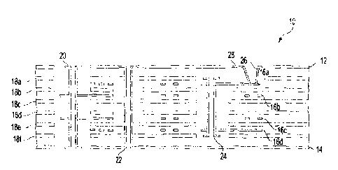
Figure 1 is a side cross-sectional view of a multilayer
printed circuit board in accordance with the present
invention.
Figure 2 shows a layout of a surface mount grid array
package of an electronic component having 1247 input/output
(I/0) contacts.
12
CA 02438751 2007-06-14
Figure 3 shows one quadrant (i.e., the lower right
quadrant) of the layout shown in Figure 2.
Figure 4 shows a portion of the primary layer of the
multilayer printed circuit board shown in Figure 1.
Figure 5 shows a portion of a first power/ground plane
layer of the multilayer printed circuit board shown in Figure
1.
Figure 6 shows a portion of a first signal layer of the
multilayer printed circuit board shown in Figure 1.
Figure 7 shows a portion of a second power/ground plane
layer of the multilayer printed circuit board shown in Figure
1.
Figure 8 shows a portion of a second signal layer of the
multilayer printed circuit board shown in Figure 1.
Figure 9 shows a portion of a third power/ground plane
layer of the multilayer printed circuit board shown in Figure
1.
Figure 10 shows a portion of a fourth power/ground plane
layer of the multilayer printed circuit board shown in Figure
1.
Figure 11 shows a portion of a third signal layer of the
multilayer printed circuit board shown in Figure 1.
Figure 12 shows a portion of a fifth power/ground plane
layer of the multilayer printed circuit board shown in Figure
1.
13
CA 02438751 2007-06-14
Figure 13 shows a portion of a fourth signal layer of the
multilayer printed circuit board shown in Figure 1.
Figure 14 shows a portion of a sixth power/ground plane
layer of the multilayer printed circuit board shown in Figure
1.
Figure 15 shows a portion of the secondary layer of the
multilayer printed circuit board shown in Figure 1.
Figure 16 shows an alternative embodiment of a portion of
the primary layer of the multilayer printed circuit board
shown in Figure 1.
Figure 17 is a side cross-sectional view of another
multilayer printed circuit board in accordance with the
present invention.
Figure 18A shows an electronic component having
electrically conductive contacts formed on one side thereof
for electrically connecting to corresponding electrically
conductive contacts formed on a layer of the multilayer
printed circuit board shown in Figure 17.
Figure 18B shows an electronic component having
electrically conductive contacts formed on multiple sides
thereof for electrically connecting to corresponding
electrically conductive contacts formed on multiple layers of
the multilayer printed circuit board shown in Figure 17.
14
CA 02438751 2007-06-14
DETAILED DESCRIPTION OF EXEMPLARY EMBODIMENT(S)
Referring to Figure 1, there is shown a side cross-
sectional view of a multilayer printed circuit board 10 in
accordance with the present invention. That is, the
multilayer printed circuit board 10 incorporates the concepts
of the present invention so as to reduce the number of layers
in the multilayer printed circuit board 10.
The multilayer printed circuit board 10 comprises a
primary (top) layer 12, a secondary (bottom) layer 14, a
plurality of signal layers 16, and a plurality of power/ground
plane layers 18. It should be noted that the primary layer 12
and the secondary layer 14 are primarily power/ground plane
layers except for contact pads and test signal runs formed
thereon, as will be described in more detail below. It should
also be noted that electronic components may be mounted on
either (single-sided board) or both (double-sided board) the
primary layer 12 and the secondary layer 14.
The multilayer printed circuit board 10 also comprises a
first supervia 20 for electrically connecting selected ones of
the plurality of signal layers 16 (i.e., signal layers 16b and
16c), a second supervia 22 for electrically connecting the
primary layer 12, the secondary layer 14, and selected ones of
the plurality of power/ground plane layers 18 (i.e.,
power/ground plane layers 18a, 18c, 18e, and 18f), a buried
via 24 for electrically connecting selected ones of the
CA 02438751 2007-06-14
plurality of signal layers 16 (i.e., signal layers 16a and
16d), and a microvia 26 for electrically connecting signal
layer 16a to a contact pad 28 formed on the primary layer 12.
It should be noted that the buried via 24 and/or the
microvia 26 may alternatively be used to electrically connect
selected ones of the plurality of power/ground plane layers
18. It should also be noted that the microvia 26 could also
be a via-in-pad, or some other similar non-through-hole via,
that the microvia 26 may be formed on either or both the
primary layer 12 and the secondary layer 14, and that the
microvia 26 may be electrically connected to other microvias,
supervias, buried vias, etc., either directly or through
signal layer or power/ground plane layer electrical
connections. It should further be noted that it is the
microvia 26 (or substantial equivalent thereof) which allows a
substantial portion of the present invention technique to be
realized, as will now be described in more detail with
reference to Figures 2-16, of which Figures 4-16 correspond to
the twelve layers of the multilayer printed circuit board 10.
Referring to Figure 2, there is shown a layout 30 of a
surface mount grid array package of an electronic component
having 1247 input/output (I/O) contacts. Figure 2 also shows
a legend indicating the type of signal associated with I/0
contact.
16
CA 02438751 2007-06-14
In order to increase the resolution for purposes of
better understanding this detailed description, Figure 3 shows
one quadrant 32 (i.e., the lower right quadrant) of the layout
30 shown in Figure 2. Figures 4-16 directly coiricide with the
quadrant 32 shown in Figure 3. The signal type legend in
Figure 2 also applies to Figure 3, as well as to Figures 4-16.
Referring to Figure 4, there is shown a portion 34 of the
primary layer 12 of the multilayer printed circuit board 10.
As indicated above, this portion 34 of the primary layer 12
directly coincides with the quadrant 32 shown in Figure 3.
That is, this portion 34 of the primary layer 12 corresponds
to the portion of the multilayer printed circuit board 10
where one quadrant of an electronic component having a surface
mount grid array package with 1247 I/0 contacts is mounted on
the multilayer printed circuit board 10.
As indicated above, the primary layer 12 is primarily a
power/ground plane layer except for contact pads and test
signal runs formed thereon. More particularly, the primary
layer 12 includes a ground plane that is electrically
connected to ground contact pads (i.e., GND in legend), but is
not electrically connected to power contact pads (i.e., vdd
and Vdd2 in legend), signal contact pads (i.e., signal in
legend), or test contact pads (i.e., test in legend). The
ground plane of the primary layer 12 is also not electrically
17
CA 02438751 2007-06-14
connected to a plurality of test signal runs 36 formed on the
primary layer 12.
Also shown in Figure 4 are areas 38 of the multilayer
printed circuit board 10 where channels are formed in other
layers of the multilayer printed circuit board 10 in
accordance with the present invention. These areas 38 also
indicate where microvias or via-in-pads are formed in the
multilayer printed circuit board 10. That is, all of the
contact pads within these areas 38 are formed as microvias or
via-in-pads for facilitating the formation of channels in
other layers of the multilayer printed circuit. board 10 in
accordance with the present invention, as described in detail
below.
Referring to Figure 5, there is shown a portion 40 of the
power/ground plane layer 18a of the multilayer pr_inted circuit
board 10. As indicated above, this portion 40 of the
power/ground plane layer 18a directly coincides with the
quadrant 32 shown in Figure 3. That is, this portion 40 of
the power/ground plane layer 18a corresponds to the portion of
the multilayer printed circuit board 10 where one quadrant of
an electronic component having a surface mount grid array
package with 1247 I/O contacts is mounted on the multilayer
printed circuit board 10.
The power/ground plane layer 18a is primarily a ground
plane layer except for vias formed therein. More
18
CA 02438751 2007-06-14
particularly, the power/ground layer 18a includes a ground
plane that is electrically connected to ground vias (i.e., GND
in legend), but is not electrically connected to power vias
(i.e., Vdd and Vdd2 in legend) or signal vias (i.e., signal in
legend). Note that there are no test vias formed in the
power/ground plane layer 18a as test contact pads and test
signal runs are typically only formed on the primary layer 12.
Also shown in Figure 5 are the areas 38 of the multilayer
printed circuit board 10 where channels are formed in other
layers of the multilayer printed circuit board 10 in
accordance with the present invention. Again, these areas 38
also indicate where microvias or via-in-pads are formed in the
multilayer printed circuit board 10. That is, all of the vias
within these areas 38 are formed as microvias or via-in-pads
for facilitating the formation of channels in other layers of
the multilayer printed circuit board 10 in accordance with the
present invention, as described in detail below.
Referring to Figure 6, there is shown a portion 42 of the
signal layer 16a of the multilayer printed circuit board 10.
As indicated above, this portion 42 of the sigrial layer 16a
directly coincides with the quadrant 32 shown in Figure 3.
That is, this portion 42 of the power/ground plane layer 18a
corresponds to the portion of the multilayer printed circuit
board 10 where one quadrant of an electronic component having
a surface mount grid array package with 1247 I/U contacts is
19
CA 02438751 2007-06-14
mounted on the multilayer printed circuit board 10.
The signal layer 16a includes a plurality of electrically
conductive signal runs 44 that are electrically connected to
the microvias or via-in-pads in the areas 38 of the multilayer
printed circuit board 10 where channels are formed in other
layers of the multilayer printed circuit board 10 in
accordance with the present invention. These signal runs 44
are typically preselected based upon the characteristics of
the signals they carry. That is, the signals runs 44 may
carry high speed signals. Alternatively, the signals runs 44
may carry low speed signals. Importantly, the microvias or
via-in-pads that are formed in the areas 38 of t:he multilayer
printed circuit board 10 do not extend any further into the
multilayer printed circuit board 10 than the signal layer 16a.
This allows channels to be formed beneath these microvias or
via-in-pads in other layers of the multilayer pr=inted circuit
board 10, as described in detail below.
Referring to Figure 7, there is shown a portion 46 of the
power/ground plane layer 18b of the multilayer printed circuit
board 10. As indicated above, this portion 46 of the
power/ground plane layer 18b directly coincides with the
quadrant 32 shown in Figure 3. That is, this portion 46 of
the power/ground plane layer 18b corresponds to the portion of
the multilayer printed circuit board 10 where one quadrant of
an electronic component having a surface mount grid array
CA 02438751 2007-06-14
package with 1247 I/0 contacts is mounted on the multilayer
printed circuit board 10.
The power/ground plane layer 18b is primarily a power
plane layer except for vias formed therein. More
particularly, the power/ground layer 18b includes a power
plane that is electrically connected to power vj_as ( i. e., Vdd
in legend), but is not electrically connected to ground vias
(i.e., GND in legend) or signal vias (i.e., signal in legend).
Note that there are no test vias formed in the power/ground
plane layer 18b as test contact pads and test signal runs are
typically only formed on the primary layer 12. Also note that
there are no vias formed in the power/ground plane layer 18b
in the areas 38 of the multilayer printed circuit board 10,
thereby forming channels in these areas 38 in this and other
layers of the multilayer printed circuit board 10 in
accordance with the present invention. These areas 38 of the
multilayer printed circuit board 10 are devoid of vias in the
power/ground plane layer 18b because microvias or via-in-pads
are only formed in these areas 38 of the multilayer printed
circuit board 10 extending from the primary layer 12 to the
signal layer 16a, as described above.
Referring to Figure 8, there is shown a portion 48 of the
signal layer 16b of the multilayer printed circuit board 10.
As indicated above, this portion 48 of the signal layer 16b
directly coincides with the quadrant 32 shown in Figure 3.
21
CA 02438751 2007-06-14
That is, this portion 48 of the signal layer 16b corresponds
to the portion of the multilayer printed circuit board 10
where one quadrant of an electronic component having a surface
mount grid array package with 1247 I/0 contacts is mounted on
the multilayer printed circuit board 10.
The signal layer 16b includes a plurality of electrically
conductive signal runs 50 that are electrically connected to
vias formed in the signal layer 16b outside the areas 38 of
the multilayer printed circuit board 10 where channels are
formed in this and other layers of the multilayer printed
circuit board 10. In accordance with the present invention,
many of these signal runs 50 are routed in these channels.
That is, the channels formed by the absence of vias in the
signal layer 16b in the areas 38 of the multilayer printed
circuit board 10 allow the plurality of electrically
conductive signal runs 50 to be routed therein. Otherwise, if
vias were present in these areas 38 in this and other layers
of the multilayer printed circuit board 10, then additional
signal layers would be required to route the plurality of
electrically conductive signal runs 50. Thus, the absence of
vias in these areas 38 in this and other layers of the
multilayer printed circuit board 10 allow for an overall
reduction in the number of signal layers required in the
multilayer printed circuit board 10.
22
CA 02438751 2007-06-14
At this point it should be noted that the channels formed
in the areas 38 of the multilayer printed circuit board 10 are
beneficially arranged so as to intersect at least one edge of
the grid array. The benefit of this arrangement is to allow
the plurality of electrically conductive signal runs 50 to be
more easily routed out from within the grid array. In fact,
as shown in Figure 8, some of the channels formed in the areas
38 of the multilayer printed circuit board 10 intersect more
than one edge of the grid array. These multiple edge
intersecting channels are typically formed of orthogonal
columns and rows, but may also be formed in diagonal or random
patterns.
It should also be noted that the channels formed in the
areas 38 of the multilayer printed circuit board 10 may have
varying widths. That is, while the channels formed in the
areas 38 of the multilayer printed circuit board 10 are shown
in Figure 8 as having a width of one contact pad or via, the
present invention is not limited in this regard. For example,
the channels formed in the areas 38 of the multilayer printed
circuit board 10 can be two or more contact pads or vias wide
depending upon how many microvias or via-in-pads are used and
how many vias are removed in accordance with the practices of
the present invention as described above.
Referring to Figure 9, there is shown a portion 52 of the
power/ground plane layer 18c of the multilayer printed circuit
23
CA 02438751 2007-06-14
board 10. As indicated above, this portion 52 of the
power/ground plane layer 18c directly coincides with the
quadrant 32 shown in Figure 3. That is, this portion 52 of
the power/ground plane layer 18c corresponds to the portion of
the multilayer printed circuit board 10 where one quadrant of
an electronic component having a surface mount grid array
package with 1247 I/0 contacts is mounted on the multilayer
printed circuit board 10.
The power/ground plane layer 18c is primarily a ground
plane layer except for vias formed therein. More
particularly, the power/ground layer 18c includes a ground
plane that is electrically connected to ground vias (i.e., GND
in legend), but is not electrically connected to power vias
(i.e., Vdd and Vdd2 in legend) or signal vias (i.e., signal in
legend). Note that there are no test vias formed in the
power/ground plane layer 18c as test contact pads and test
signal runs are typically only formed on the primary layer 12.
Also note that there are no vias formed in the power/ground
plane layer 18c in the areas 38 of the multilayer printed
circuit board 10, thereby forming channels in these areas 38
in this and other layers of the multilayer printed circuit
board 10 in accordance with the present invention. These
areas 38 of the multilayer printed circuit board 10 are devoid
of vias in the power/ground plane layer 18c because microvias
or via-in-pads are only formed in these areas 38 of the
24
CA 02438751 2007-06-14
multilayer printed circuit board 10 extending from the primary
layer 12 to the signal layer 16a, as described above.
Referring to Figure 10, there is shown a portion 54 of
the power/ground plane layer 18d of the multilayer printed
circuit board 10. As indicated above, this portion 54 of the
power/ground plane layer 18d directly coincides with the
quadrant 32 shown in Figure 3. That is, this portion 54 of
the power/ground plane layer 18d corresponds to the portion of
the multilayer printed circuit board 10 where one quadrant of
an electronic component having a surface mount grid array
package with 1247 I/0 contacts is mounted on the multilayer
printed circuit board 10.
Similar to power/ground plane layer 18b, the power/ground
plane layer 18d is primarily a power plane layer except for
vias formed therein. More particularly, the power/ground
layer 18d includes a power plane that is electrically
connected to power vias (i.e., Vdd2 in legend), but is not
electrically connected to ground vias (i.e., GND in legend) or
signal vias (i.e., signal in legend). Note that there are no
test vias formed in the power/ground plane layer 18d as test
contact pads and test signal runs are typically only formed on
the primary layer 12. Also note that there are no vias formed
in the power/ground plane layer 18d in the areas 38 of the
multilayer printed circuit board 10, thereby forining channels
in these areas 38 in this and other layers of the multilayer
CA 02438751 2007-06-14
printed circuit board 10 in accordance with the present
invention. These areas 38 of the multilayer printed circuit
board 10 are devoid of vias in the power/ground plane layer
18d because microvias or via-in-pads are only formed in these
areas 38 of the multilayer printed circuit board 10 extending
from the primary layer 12 to the signal layer 16a, as
described above.
Referring to Figure 11, there is shown a portion 56 of
the signal layer 16c of the multilayer printed circuit board
10. As indicated above, this portion 56 of the signal layer
16c directly coincides with the quadrant 32 shown in Figure 3.
That is, this portion 56 of the signal layer 16c corresponds
to the portion of the multilayer printed circuit board 10
where one quadrant of an electronic component having a surface
mount grid array package with 1247 I/0 contacts is mounted on
the multilayer printed circuit board 10.
The signal layer 16c includes a plurality of electrically
conductive signal runs 58 that are electrically connected to
vias formed in the signal layer 16c outside the areas 38 of
the multilayer printed circuit board 10 where channels are
formed in this and other layers of the multilayer printed
circuit board 10. In accordance with the present invention,
many of these signal runs 58 are routed in these channels.
That is, the channels formed by the absence of vias in the
signal layer 16c in the areas 38 of the multilayer printed
26
CA 02438751 2007-06-14
circuit board 10 allow the plurality of electrically
conductive signal runs 58 to be routed therein. Otherwise, if
vias were present in these areas 38 in this and other layers
of the multilayer printed circuit board 10, then additional
signal layers would be required to route the plurality of
electrically conductive signal runs 58. Thus, the absence of
vias in these areas 38 in this and other layers of the
multilayer printed circuit board 10 allow for an overall
reduction in the number of signal layers required in the
multilayer printed circuit board 10.
Referring to Figure 12, there is shown a portion 60 of
the power/ground plane layer 18e of the multilayer printed
circuit board 10. As indicated above, this portion 60 of the
power/ground plane layer 18e directly coincides with the
quadrant 32 shown in Figure 3. That is, this portion 60 of
the power/ground plane layer 18e corresponds to the portion of
the multilayer printed circuit board 10 where orie quadrant of
an electronic component having a surface mour.it grid array
package with 1247 I/O contacts is mounted on the multilayer
printed circuit board 10.
Similar to power/ground plane layer 18c, the power/ground
plane layer 18e is primarily a ground plane layer except for
vias formed therein. More particularly, the power/ground
layer 18e includes a ground plane that is electrically
connected to ground vias (i.e., GND in legend), but is not
27
CA 02438751 2007-06-14
electrically connected to power vias (i.e., Vdd and Vdd2 in
legend) or signal vias (i.e., signal in legend). Note that
there are no test vias formed in the power/ground plane layer
18e as test contact pads and test signal runs are typically
only formed on the primary layer 12. Also note that there are
no vias formed in the power/ground plane layer 18e in the
areas 38 of the multilayer printed circuit board 10, thereby
forming channels in these areas 38 in this and other layers of
the multilayer printed circuit board 10 in accordance with the
present invention. These areas 38 of the multilayer printed
circuit board 10 are devoid of vias in the power/ground plane
layer 18e because microvias or via-in-pads are only formed in
these areas 38 of the multilayer printed circuit board 10
extending from the primary layer 12 to the signal layer 16a,
as described above.
Referring to Figure 13, there is shown a portion 62 of
the signal layer 16d of the multilayer printed circuit board
10. As indicated above, this portion 62 of the signal layer
16d directly coincides with the quadrant 32 shown in Figure 3.
That is, this portion 62 of the signal layer 16d corresponds
to the portion of the multilayer printed circuit board 10
where one quadrant of an electronic component having a surface
mount grid array package with 1247 I/0 contacts is mounted on
the multilayer printed circuit board 10.
The signal layer 16d includes a plurality of electrically
28
CA 02438751 2007-06-14
conductive signal runs 64 that are electrically connected to
vias formed in the signal layer 16d outside the areas 38 of
the multilayer printed circuit board 10 where channels are
formed in this and other layers of the multilayer printed
circuit board 10. In accordance with the present invention,
many of these signal runs 64 are routed in these channels.
That is, the channels formed by the absence of vias in the
signal layer 16d in the areas 38 of the multilayer printed
circuit board 10 allow the plurality of electrically
conductive signal runs 64 to be routed therein. Otherwise, if
vias were present in these areas 38 in this and other layers
of the multilayer printed circuit board 10, then additional
signal layers would be required to route the plurality of
electrically conductive signal runs 64. Thus, the absence of
vias in these areas 38 in this and other layers of the
multilayer printed circuit board 10 allow for an overall
reduction in the number of signal layers required in the
multilayer printed circuit board 10.
Referring to Figure 14, there is shown a portion 66 of
the power/ground plane layer 18f of the multilayer printed
circuit board 10. As indicated above, this portion 66 of the
power/ground plane layer 18f directly coincides with the
quadrant 32 shown in Figure 3. That is, this portion 66 of
the power/ground plane layer 18f corresponds to the portion of
the multilayer printed circuit board 10 where one quadrant of
29
CA 02438751 2007-06-14
an electronic component having a surface mount grid array
package with 1247 I/0 contacts is mounted on the multilayer
printed circuit board 10.
Similar to power/ground plane layers 18c and 18e, the
power/ground plane layer 18f is primarily a ground plane layer
except for vias formed therein. More particularly, the
power/ground layer 18f includes a ground plane that is
electrically connected to ground vias (i.e., GND in legend),
but is not electrically connected to power vias (i.e., Vdd and
Vdd2 in legend) or signal vias (i.e., signal in legend). Note
that there are no test vias formed in the power/ground plane
layer 18f as test contact pads and test signal runs are
typically only formed on the primary layer 12. Also note that
there are no vias formed in the power/ground plane layer 18f
in the areas 38 of the multilayer printed circuit board 10,
thereby forming channels in these areas 38 in this and other
layers of the multilayer printed circuit board 10 in
accordance with the present invention. These areas 38 of the
multilayer printed circuit board 10 are devoid of vias in the
power/ground plane layer 18f because microvias or via-in-pads
are only formed in these areas 38 of the multilayer printed
circuit board 10 extending from the primary layer 12 to the
signal layer 16a, as described above.
Referring to Figure 15, there is shown a portion 68 of
the secondary layer 14 of the multilayer printed circuit board
CA 02438751 2007-06-14
10. As indicated above, this portion 68 of the secondary
layer 14 directly coincides with the quadrant 32 shown in
Figure 3. That is, this portion 68 of the secondary layer 14
corresponds to the portion of the multilayer printed circuit
board 10 where one quadrant of an electronic conlponent having
a surface mount grid array package with 1247 I/0 contacts is
mounted on the multilayer printed circuit board 10.
As indicated above, the secondary layer 14 is primarily a
power/ground plane layer except for contact pads formed
thereon. More particularly, the secondary layer 14 includes a
ground plane that is electrically connected to ground contact
pads (i.e., GND in legend), but is not electrically connected
to power contact pads (i.e., Vdd and Vdd2 in legend) or signal
contact pads (i.e., signal in legend). Note that there are no
test vias formed in the secondary layer 14 as test contact
pads and test signal runs are typically only formed on the
primary layer 12. Also note that there are no vias formed in
the secondary layer 14 in the areas 38 of the multilayer
printed circuit board 10, thereby forming chanriels in these
areas 38 in this and other layers of the multilayer printed
circuit board 10 in accordance with the present invention.
These areas 38 of the multilayer printed circuit board 10 are
devoid of vias in the secondary layer 14 because microvias or
via-in-pads are only formed in these areas 38 of the
multilayer printed circuit board 10 extending from the primary
31
CA 02438751 2007-06-14
layer 12 to the signal layer 16a, as described above.
At this point it should be noted that the above-described
techniques for reducing the number of layers in a multilayer
printed circuit board have been substantially described in the
above-referenced U.S. Patent Application No. 10/126,700, U.S.
Patent Application No. 09/651,188 (now U.S. Patent No.
6,388,890), and U.S. Provisional Patent Application No.
60/212,387. Also, related techniques for reducing the number
of layers in a multilayer printed circuit board have been
substantially described in the above-referenced U.S. Patent
Application No. 10/101,211, (now U.S. Patent No. TBA), U.S.
Patent Application No. 09/651,188 (now U.S. Patent No.
6,388,890), and U.S. Provisional Patent Application No.
60/212,387. All of these techniques may be implemented either
manually or in an automated manner. For example, these
techniques may be automated by receiving electronic component
information in, for example, a design file. That is, the
design file may include an electrically conductive contact
count characteristic, an electrically conductive contact pitch
characteristic, an electrically conductive contact signal type
characteristic, and/or an electrically conductive contact
signal direction characteristic for one or more electronic
components. One or more electronic components having a high
32
CA 02438751 2007-06-14
density electrically conductive contact array package may
then be identified based at least in part upon at least one of
the electrically conductive contact count characteristic or
the electrically conductive contact pitch characteristic.
Electrical signals may then be routed on a plurality of
electrically conductive signal path layers in a multilayer
circuit board so as to make electrical connections to and from
each high density electrically conductive contact array
package that is mounted on the multilayer circuit board based
at least in part upon at least one of the electrically
conductive contact signal type characteristic or the
electrically conductive contact signal direction
characteristic.
Thus, at this point it should be noted that reducing the
number of layers in a multilayer printed circuit board in
accordance with the present invention as described above may
involve the processing of input data and the generation of
output data to some extent. This input data processing and
output data generation may be implemented in hardware or
software. For example, specific electronic and/or optical
components may be employed in a processing device or similar
or related circuitry for implementing the functions associated
with reducing the number of layers in a multilayer printed
circuit board in accordance with the present invention as
described above. Alternatively, one or more processors
33
CA 02438751 2007-06-14
operating in accordance with stored instructions may implement
the functions associated with reducing the number of layers in
a multilayer printed circuit board in accordance with the
present invention as described above. If such is the case, it
is within the scope of the present invention that such
instructions may be stored on one or more processor readable
carrier (e.g., a magnetic disk), or transmitted to one or more
processors via one or more signals.
At this point it should be noted that, along the lines of
that described in the above-referenced U.S. Patent Application
No. 10/126,700, U.S. Patent Application No. 09/651,188 (now
U.S. Patent No. 6,388,890), and U.S. Provisional Patent
Application No. 60/212,387, all of which have been
incorporated by reference herein in their entirety, one or
more microvias 26 may be formed in the multilayer circuit
board 10 extending from the surface 12 of the multilayer
circuit board 10 to one of the plurality of electrically
conductive signal path layers (e.g., 16b), wherein the
microvias 26 are arranged so as to form at least one of the
channels 38 in another of the plurality of electrically
conductive signal path layers (e.g., 16c) located beneath the
microvias 26. That is, one or more microvias 26 may extend
from the surface 12 of the multilayer circuit board 10 to
others of the plurality of electrically conductive signal path
34
CA 02438751 2007-06-14
layers (e.g., 16b, 16c, 16d) besides the uppermost
electrically conductive signal path layer (i.e., 16a).
At this point it should be noted that the channels 38 may
be configured to have a linear, circular, diamond, curved,
stepped, staggered, and/or random shape, or a combination
thereof. Also, the channels 38 may be configured to be in a
vertical, horizontal, diagonal, and/or random direction, or a
combination thereof. Further, one or more channels 38 may be
formed such that they are totally enclosed withir.L the array of
electrically conductive contacts that are formed on the
multilayer circuit board 10 for mating with the electrically
conductive contacts of the electronic component (i.e., no
portion of the channel is formed along the periphery of the
array of electrically conductive contacts formed on the
multilayer circuit board 10)(e.g., see channel 38a in Figure
16). Additionally, one or more channels 38 may be formed such
that they extend all the way across the array of electrically
conductive contacts that are formed on the multi.layer circuit
board 10 for mating with the electrically conductive contacts
of the electronic component (i.e., the channel is formed
extending from one side to another side of the array of
electrically conductive contacts formed on the multilayer
circuit board 10). Moreover, one or more channels 38 may be
formed such that only portions thereof extend to the periphery
of the array of electrically conductive contacts that are
CA 02438751 2007-06-14
formed on the multilayer circuit board 10 for mating with the
electrically conductive contacts of the electronic component
(i.e., at least a portion of the channel is formed along the
periphery of the array of electrically conductive contacts
formed on the multilayer circuit board 10).
At this point it should be noted that the electrically
conductive contacts of the electronic component, and thus the
array of electrically conductive contacts that are formed on
the multilayer circuit board 10 for mating with the
electrically conductive contacts of the electronic component,
may have a variety of contact array patterns. For example,
the electrically conductive contacts of the electronic
component, and hence the array of electrically conductive
contacts formed on the multilayer circuit board :LO, may have a
square, triangular, circular, and/or random electrically
conductive contact pattern, or a combination thereof.
At this point it should be noted that at least some of
the electrical signals to be routed may be differential
electrical signals. If such is the case, the differential
electrical signals may beneficially be at least partially
routed together in the channels 38 formed in the plurality of
electrically conductive signal path layers 16 beneath the
microvias 26, thereby enhancing signal quality.
At this point it should be noted that it may be
beneficial to form at least some of the microvias 26 outside
36
CA 02438751 2007-06-14
of the array of electrically conductive contacts that are
formed on the multilayer circuit board 10 for mating with the
electrically conductive contacts of the electronic component.
For example, referring to Figure 16, there is shown an
alternative embodiment of a portion 34a of the primary layer
12 of the multilayer printed circuit board 10 wherein some of
the microvias 26a are formed outside of the array of
electrically conductive contacts that are formed on the
multilayer circuit board 10 for mating with the electrically
conductive contacts of the electronic component. The
microvias 26a are electrically connected to corresponding
peripheral ones of the electrically conductive array contacts
that are formed on the multilayer circuit board 10 for mating
with the electrically conductive contacts of the electronic
component via electrically conductive connections 70. As
discussed above, the microvias 26a may extend from the surface
12 of the multilayer circuit board 10 to any of the plurality
of electrically conductive signal path layers 16. However,
the peripheral electrically conductive array contacts that are
connected to the microvias 26a do not extend below the primary
layer 12 of the multilayer printed circuit board 10. Thus,
additional and/or expanded channels 38a may be formed in all
of the plurality of electrically conductive signal path layers
16 beneath these peripheral electrically conductive array
37
CA 02438751 2007-06-14
contacts, including the uppermost electrically conductive
signal path layer (i.e., 16a).
At this point it should be noted that, along the lines of
that described in the above-referenced U.S. Patent Application
No. 10/101,211, (now U.S. Patent No. TBA), U.S. Patent
Application No. 09/651,188 (now U.S. Patent No. 6,388,890),
and U.S. Provisional Patent Application No. 60/212,387, one or
more electrically conductive vias may be formed in the
multilayer printed circuit board 10 extending from the surface
12 of the multilayer printed circuit board 10 to at least one
of the electrically conductive power/ground layers (i.e., 18
and/or 14), wherein each of the electrically conductive vias
is electrically connected to at least one respective
electrically conductive power/ground contact formed on the
surface 12 of the multilayer printed circuit board 10. Each
of the electrically conductive power/ground contacts forms a
portion of the electrically conductive contact array that is
formed on the surface 12 of the multilayer circuit board 10
for mating with the electrically conductive power/ground
contacts of the electronic component. This allows additional
channels to be formed in each of the plurality of electrically
conductive signal path layers 16 beneath the electrically
conductive power/ground contacts.
38
CA 02438751 2007-06-14
At this point it should be noted that all of the above-
described variations and benefits associated with reducing the
number of layers in a multilayer printed circuit board using
microvias may also be implemented and obtained using
electrically conductive vias that are electrically connected
to electrically conductive power/ground contacts, as described
above.
At this point it should be noted that, while the above
detailed description has thus far been limited to reducing the
number of layers in a multilayer printed circuit board having
electronic components mounted thereon, it is well within the
scope of the present invention to apply the above-described
techniques to a multilayer printed circuit board having a wide
variety of electronic components embedded therein. For
example, referring to Figure 17, there is shown a side cross-
sectional view of an alternative multilayer printed circuit
board 10a in accordance with the present invention. Similar
to the multilayer printed circuit board 10 of Figure 1, the
multilayer printed circuit board 10a of Figure 17 comprises a
primary (top) layer 12, a secondary (bottom) layer 14, a
plurality of signal layers 16, and a plurality of power/ground
plane layers 18. The multilayer printed circuit board 10a
also comprises a supervia 20 for electrically connecting the
primary layer 12, the secondary layer 14, and selected ones of
the plurality of power/ground plane layers 18. The multilayer
39
CA 02438751 2007-06-14
printed circuit board 10a further comprises a plurality of
buried vias 24 for electrically connecting selected ones of
the plurality of signal layers 16 and selected ones of the
plurality of power/ground plane layers 18.
Differing from the multilayer printed circuit board 10 of
Figure 1, the multilayer printed circuit board 10a of Figure
17 comprises a blind via 74 for electrically connecting the
secondary layer 14, selected ones of the plurality of signal
layers 16, and selected ones of the plurality of power/ground
plane layers 18. The multilayer printed circluit board 10a
also comprises an embedded electronic component 72 disposed
between the power/ground plane layer 18a and the signal layer
16a.
As mentioned above, the embedded electronic component 72
may be one of a wide variety of possible electronic
components. For example, referring to Figure 18A, there is
shown an electronic component 72a having electrically
conductive contacts 76 formed on one side thereof. In this
case, the electrically conductive contacts 76 may electrically
connect to corresponding electrically conductive contacts
formed on a selected one of the plurality of signal layers 16
(i.e., layer 16a in Figure 17) or a selected one of the
plurality of power/ground plane layers 18 (i.e., layer 18a in
Figure 17). Alternatively, referring to Figure 18B, there is
shown an electronic component 72b having electrically
CA 02438751 2007-06-14
conductive contacts 76 formed on both sides thereof. In this
case, the electrically conductive contacts 76 may electrically
connect to corresponding electrically conductive contacts
formed on a selected one of the plurality of signal layers 16
(i.e., layer 16a in Figure 17) and a selected one of the
plurality of power/ground plane layers 18 (i.e., layer 18a in
Figure 17). Of course, other types of electronic components
(e.g., discrete components) may be embedded in the multilayer
printed circuit board 10a of Figure 17, and such embedded
electronic components may be disposed between or on any of the
plurality of signal layers 16 and/or any of the plurality of
power/ground plane layers 18 in accordance with the present
invention. In any case, the above-described techniques for
reducing the number of layers in a multilayer printed circuit
board may apply when such embedded electronic components are
employed.
At this point it should be noted that, while the above
detailed description has thus far been limited to reducing the
number of layers in a multilayer printed circuit board, it is
well within the scope of the present invention to apply the
above-described techniques to a wide variety of multilayer
signal routing devices. For example, the above-described
techniques may be applied to multilayer integrated circuit die
packaging devices. Thus, the present invention is more
appropriately directed to techniques for reducing the number
41
CA 02438751 2007-06-14
of layers in a multilayer signal routing device.
The present invention is not to be limited in scope by
the specific embodiments described herein. Indeed, various
modifications of the present invention, in addition to those
described herein, will be apparent to those of ordinary skill
in the art from the foregoing description anci accompanying
drawings. Thus, such modifications are intended to fall
within the scope of the following appended claims. Further,
although the present invention has been described herein in
the context of a particular implementation in a particular
environment for a particular purpose, those of ordinary skill
in the art will recognize that its usefulness is not limited
thereto and that the present invention can be beneficially
implemented in any number of environments for any number of
purposes. Accordingly, the claims set forth below should be
construed in view of the full breath and spirit of the present
invention as disclosed herein.
42