Note: Descriptions are shown in the official language in which they were submitted.
CA 02438777 2003-08-29
RADIATION DETECTOR
BACKGROUND OF THE INVENTION
(1) Field of the Invention
a This invention relates to a radiation detector for
measuring a spatial distribution of radiation in the medical,
industrial, nuclear and other fields.
(2) Description of the Related Art
A known radiation detector has a common electrode
to formed on one surface of a semiconductor sensitive to radia-
tion, with a bias voltage applied to the common electrode,
and a plurality of split electrodes formed on the other
surface of the semiconductor. Incident radiation generates
electric charges within the semiconductor, and these charges
15 are fetched through the respective split electrodes as electric
signals. In this way, the radiation detector detects a
spatial distribution of incident radiation. Such radiation
detectors may be manufactured in various ways which may.
broadly, be classified into the following three methods.
2o Firstly, a semiconductor film is formed on a
substrate having split electrodes formed thereon beforehand,
and then a common electrode is formed on the
semiconductor film. Secondly, a semiconductor film :ia
formed on a substrata having a common electrode formed
25 thereon beforehand, and then split electrodes are formed on
1-
CA 02438777 2003-08-29
the semiconductor film. Thirdly, a common electrode is
formed on one sur~.face of a semiconductor crystal substrate,
and split electrodes are formed on the other surface of the
substrate.
The detector manufactured by the first method has a.
substrate disposed on the split electrode side. The other
two types of detectors, genes°ally, are also used by connecting
the split electrodes to an electronic circuit board for
processing signals. Since each of the above three types has
to a substrate disposed on the split electrode side, the
conventional radiation detector generally detects radiation
incident on the common electrode side.
The conventional detector constructed as described
above has the following drawbacks.
1:; The conventional radiation detector noted above has
no electrodes for sweeping out the charges having been
moved by an electric field to regions of space between the
split electrodes. The charges generated by radiation tend
to collect in those regions. Consequently, lines of electric
20 force are distorted to vary ;gin effective sensitive area,
resulting in a sensitivity variation phenomenon. In this
case, also after cessation of the incident radiation, the
charges having collected in the regions of space between the
split electrodes are gradually swept out to cause an
25 undesi~~able phenomenon of after-output.
CA 02438777 2003-08-29
Furthermore, when an incidence of radiation takes
place at a higher r ate than a charge sweep-out, the charges
collect also in regions having the split electrodes formed
therein. This distorts an electric potential profile in the
semiconductor to raise the electric potentials adjacent the
split electrodes. In one example, an amorphous selenium
(a-Se) film and a common electrode are formed on a
substrate having a plurality of split electrodes and thin film
transistors (TFT), and signals are successively read by
switching operation of the TFTs. In this particular case, a
high bias must be applied to the a-Se in use, and the
potential rise adjacent the split electrodes becomes high
enough to influence the switching operation of the TFTs.
This results in phenomena such as of slow reading operation,
and causes sensibility variations or after-outputs.
The above two phenomena will particularly be
described hereinafter with reference to Figs. 1 and 2. Figs.
1 and 2 are sectional views schematically illustrating
interior conditions of a conventional radiation detector'.
hig. 1A is a schematic view showing a state before an
incidence of radiation. In this state, all lines of electric
force run parallel inside a thick semiconductor film 51.
Where each split electrode 53 has a width "a" and a length
"y" in the direction of depth, a sensitive area is "axy". l~~ig.
2p 1B is a schematic view showing a state occurring with an
CA 02438777 2003-08-29
incidence of radiation. Of the charges (electrons and holes)
generated in regions of space between the split electrodes 53,
the charges (e.g. holes in Fig. 1B) moving toward the side
having the split electrodes 53 are captured to stagnate (as at
a 55) adjacent surfaces of the thick semiconductor film 51, in
the absence of electrodes for sweeping out the holes. In this
way, the holes collect gradually to distort the lines of electric
force in the thick semiconductor film 51. Where a space
between each adjacent pair of split electrodes 53 has a width
"b" and "z" in the direction of depth, a sensitive area in this
case will be (a+b) x (y+z). Therefore, sensibility is varied
(i.e. increased) from a x y to (a+b) x (y+z) until the region of
space between the split electrodes 53 is filled with the
charges.
hig. 2 shows a construction having an amorphous
selenium (a-Se) film 65 and a common electrode 67 for med
on a substrate 63 having a plurality of split electrodes 61
and thin film transistor (TFT) switches. The TFT switches
are operable for successively reading signals. The
amorphous selenium film has a thickness d. In Fig. 2A,
which is a schematic: view showing a state before an
incidence of radiation, an electric potential adjacent the split
electrodes 61 is sufficiently low. However, when an
incidence of radiation takes place at a higher r ate than the
charge sweep-out, the charges c:ollect adjacent the split
-4-
CA 02438777 2003-08-29
73454-22
electrodes 61. This distorts the electric potential profile to
raise the electric potential adjacent the split electrodes 61
as shown in Fig. 2B. Since a high bias must be applied to
the amorphous selenium film in use, the potential rise
becomes high enough to cause malfunctioning of the TFT
switches. This results in phenomena such as of slow
reading operation, and causes sensibility variations or after-
outputs.
Such sensibility variations make a quantitative
1 o radiation detection impossible. Moreover, when the detector
is used for detecting a dynamic image, a phenomenon of
gradual brightness variations occurs, and incident radiation
doses cause different sensitivity variation curves, resulting
in a phenomenon in which an image of a preceding frame
~ 5 remains as an after-image.
SUMMARY OF THE INVENTION
This invention has been made having regard to
the state of the art noted above, and its object is to provide
2 ~ a radiation detector having split electrodes and free from
sensibility variations, which is achieved by stabilizing an
electric field generated in the radiation detector by light
irradiation.
According to the present invention, there is
2 5 provided a radiation detector for detecting a spatial
distribution of incident radiation, comprising a radiation-
sensitive
CA 02438777 2003-08-29
semiconductor; a common electrode formed on one surface of
the semiconductor for receiving a bias voltage; a plurality of
split electrodes for med on the other surface of the
semiconductor for outputting, as electric signals, charges
p generated within the semiconductor by the incident radia-
tion; and a light irradiating mechanism for emitting light at.
least during a detection of the radiation.
The radiation detector according to this invention
has a light irradiating mechanism for emitting light to the
to split electrode side. This mechanism emits light during a
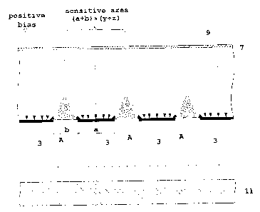
radiation detecting operation. 'Thus, as shown in Fig. 4,
charges generated by the light (i.e. holes where a positive
bias is applied to the common electrode 9) are already
collected in regions of space between the split electrodes 3.
1p Consequently, lines of electric force are distorted, and each
sensitive area is (a+b) x (y+z) from the beginning. When an
incidence of radiation takes place in this state, as Shawn in
Fig. 5, the charges moving toward the split electrodes 3, of
the charges generated in the regions of space between the
20 split elcJctrodes 3, follow the lines of electric force to reach
the split electrodes 3. No additional charges will collect in
the spaces between the split electrodes 3. Thus, no change
occurs in the state of the lines o.f electric force or the
sensitive areas, and hence no sensibility variations. The
2;p light emission may be continued after cessation of the
CA 02438777 2003-08-29
incidence of radiation. Then, the char ges collected in the
regions of space between the split electrodes 3 are not swept
out gradually, and no after-output, occurs.
The light emission or irradiation herein includes all
emission modes that produce the advantages of this inven-
tion, such as emitting light continuously or intermittently
during a detection of the radiation.
Preferably, the light has a wavelength shorter than a
wavelength corresponding to a band gap energy of the
semiconductor used.
Since the irradiating light has a wavelength shorter
than a wavelength corresponding to the band gap energy of
the semiconductor used, the irradiating light does not gene-
trate deep inside the semiconductor, but operates only in
portions very close to the surface farming the split electrodes.
The charges generated by the light collect only in limited
regions very close to the surface forming the split electrodes,
thereby reducing insensitive regions.
Further, it is preferred that the light has a wave-
length shorter than a wavelength that halves a transmit-
tance of the semiconductor used, and longer than a wave-
length c.:orresponding to a band gap energy of the
semiconductor.
Since the wavelength of the irradiating light is
2p shorter than the wavelength that halves the transmittance
_;_
CA 02438777 2003-08-29
and longer than the wavelength corresponding to the band
gap energy of the semiconductor used, part of the irradiating
light penetrates deep into the semiconductor to enlarge
insensitive regions. However, since the irradiating light
has a smaller energy than the band gap energy, the
semiconductor is free from damage (generation of crystal
defects) done by the irradiating light. No increase occurs ire
the dark current resulting from a charge detection by the
irradiating light itself. Damaging of the semiconductor by
l0 the irradiating light is conspicuous with the amorphous
semiconductor such as amorphous selenium (a-Se). This
feature is effective particularly for the radiation detector
using the amorphous semiconductor.
In another aspect of the invention, a radiation detec-
l for for detecting a spatial distribution of incident radiation,
comprises a radiation-sensitive semiconductor; a common
electrode formed on one surface of the semiconductor for
receiving a bias voltage; a plurality of split electrodes
formed on the other surface of the semiconductor for
20 outputting, as electric signals, charges generated within the
semiconductor by the incident radiation; a carrier selective
intermediate layer formed at least between the
semiconductor and the split electrodes; and a light
irradiating mechanism for emitting light at least during a
25 detection of the radiation.
CA 02438777 2003-08-29
The radiation detector having an intermediate layer
as noted above produces effects similar to those of the first
aspect of the invention.
Preferably, the light has a wavelength shorter than a.
wavelength that halves the t,ransmittance of the intermedi-
ate layer. It is more desirable that the light has a wave-
length shorter than a wavelength that reduces the transmit-
tance of i.he intermediate Iaver to 10%.
Where the intermediate layer has more defects than
to the semiconductor layer and charges tend to collect in the
intermediate layer, deflections of electric fields occur only in
the intermediate layer. Thus, also where the intermediate
layer is provided adjacent the split electrodes, the emission
of light from the side of split electrodes to the intermediate
ta> layer eliminates sensitivity variations and after-output due
to the charges collected in the regions of the intermediate
layer between the split electrodes. With the light having a
wavelength shorter than a wavelength that halves the
transmittance of the intermediate layer, a Large part of the
'~0 irradiating light is absorbed by the intermediate layer,
thereby reducing the irradiating Light reaching the
semiconductor. This provides the effect of suppressing dark
current, in the semiconductor due to the irradiating light,
besides suppressing dark current by means of the intermedi-
2~> ate layer.
_g.
CA 02438777 2003-08-29
Preferably, the semiconductor comprises an amor-
phous material selected from non-dope selenium or non-dope'
selenium compound, selenium or selenium compound doped
with As or Te, selenium doped with an alkali metal, a sele-
nium compound doped an alkali metal, selenium doped with
a halogen, a selenium compound doped with a halogen, and
selenium or selenium compound doped with a combination
of As, Te, an alkali metal and a halogen. It is also
preferable that the semiconductor comprises a
polycrystalline material different from the intermediate
layer and selected from compound semiconductors such as
CdTe, CdZnTe, PbI2, HgI2, TIBr and GaAs, and the
compound semiconductors doped with a halogen.
The intermediate layer is provided in order to reduce
dark current by using its carrier selectivity. The carrier
selectivity is a property for remarkably differentiating the
contribution to the charge transfer function between elec-
trons and holes acting as chaa°ge transfer media (carriers)
within the semiconductor.
Materials having strong carrier selectivity for
increasing the contribution of electrons are n-type
semiconductors including, :for example, polycrystals such as
CeO~, CdS, CdSe, ZnSe and ZnS, and amorphous materials
such as amorphous selenium doped with As or Te or alkali
2~ metals to lower the contribution of holes.
-10-
CA 02438777 2003-08-29
Materials for increasing the contribution of holes are
p-type semiconductors including polycrystals such as ZnTe,
and amorphous materials such as amorphous selenium
doped with halogen to lower the contribution of electrons.
Furthermore, ~b2S3, CdTe, CdZnTe, PbI~> and HgIz,
TlBr, and non-dope amorphous selenium or selenium com-
pound may increase the contribution of electrons or holes.
depending on film-forming conditions.
Where both the intermediate layer and
1c:> semiconductor Iayer a.re formed of amorphous materials, the
following combinations can be considered, for example.
Where a positive bias is applied to the common elec-
trode, an amorphous material with a large contribution of
holes is used for the intermediate layer adjacent the split
15 electrodes. This inhibits entry c>f electrons from the split
electrodes to reduce dark current. In this case, an
intermediate layer with a large contribution of electrons
may also be provided adjacent the common electrode. This
will inhibit entry of holes from the common electrode,
20 thereby further reducing dark current.
Where a negative bias is applied to the common elec-
trode, an amorphous material with a large contribution of
electrons is used for the intermediate Iayer adjacent the
split electrodes. This inhibits entry of holes from the split
2a electrodes to r educe dark cur rent. In this case, an
11-
CA 02438777 2003-08-29
intermediate layer with a large contribution of holes may
also be provided adjacent the common electrode. This will
inhibit entry of elects ons from the common electrode,
thereby further reducing dark current.
Where the semiconductor layer is an amorphous
material and the intermediate layer a polycrystal, the
following combinations are conceivable.
Where a positive bias is applied to the common elec-
trode, a polycrystal with a large contribution of holes is used
1o for the intermediate layer adjacent the split electrodes.
Where a negative bias is applied to the common electrode, a
polycrystal with a large contribution of electrons is used for
the intermediate Layer adjacent the split electrodes. In
these cases, an intermediate layer may also be provided
15 adjacent the common electrode for further reducing dark
current.
Where both the intermediate layer and
semiconductor layer are polycrystals, the following
combinations can be considered, for example.
2o Where a positive bias is applied to the common elec-
trode, a polycrystal with a large contribution of holes is used
for the intermediate layer adjacent the split electrodes.
Where a negative bias is applied to the common electrode, a
polycrystal with a large contribution of electrons is used for
?5 the intcermediate layer adjacent the split electrodes. In
CA 02438777 2003-08-29
these cases, an intermediate layer may also be provided
adjacent l;he common electrode for further reducing dark
current.
Preferably, the intermediate layer is formed on the
surface of the semiconductor having the split electrodes, by
using a material having a threshold wavelength of transmit-
tance between a wavelength that halves a transmittance
and a wavelength corresponding to a band gap energy of the
semiconductor.
to The intermediate layer formed on the surface of the
semiconductor having the split electrodes, by using a mate-
rial having a threshold wavelength of transrnittance
between a wavelength that halves a transmittance and a
wavelength corresponding to a band gap energy of the
semiconductor, has a filtering effect to produce the above
effects without limiting the wavelength of irradiating light.
Preferably, the split electrodes are transparent or
translucent to the irradiating light.
:iince the split electrodes are transparent or translu-
cent, the light irr adiates not only the regions of space
between the split electrodes, but also electrode forming
regions. Even when an incidence of radiation takes place at;
a higher rate than a charge sweep-out so that the charges
once collect adjacent the split electrodes, the energy of the
2~:o irradiating light excites the charges immediately again to
- 13-
CA 02438777 2003-08-29
;3454-22
give kinetic energy thereto. Consequently, the electric
potential profile is not distorted, and no increase occurs
with the potential adjacent the split electrodes. Thus, even
with the a-Se film requiring application of a high bias
voltage in use, the TFT switches can maintain a normal
operation.
BRIEF DESCRIPTION OF THE DRAWINGS
Examples of embodiments of the present
o invention will now be described with reference to the
drawings, in which:
Fig. 1 shows schematic views illustrating a first
problem of a conventional radiation detector, in which Fig.
1A shows a state before an incidence of radiation, and Fig.
1 B shows a state during an incidence of radiation;
Fig. 2 shows schematic views illustrating a
second problem of a conventional radiation detector, in
which Fig. 2A shows a state before an incidence of
radiation, and Fig. 2B shows a state during an incidence of
2 U radiation;
Fig. 3 is a view in vertical section showing an
outline of a radiation detector according to an embodiment
of this invention;
Fig. 4 is a schematic view showing a state before
2 5 an incidence of radiation, for illustrating a first function of
the radiation detector according to an embodiment of this
invention;
- 14 -
CA 02438777 2003-08-29
13454-22
Fig. 5 is a schematic view showing a state during
an incidence of radiation, for illustrating the first function of
the radiation detector according to an embodiment of this
invention;
Fig. 6 is a schematic view showing a state during
an irradiation with light having a wavelength shorter than a
wavelength corresponding to a band gap, for illustrating the
first function of the radiation detector according to an
embodiment of this invention;
Fig. 7 is a view illustrating a second function of
the radiation detector according to an embodiment of this
invention;
Fig. 8 is a timing chart showing an example of
control of light irradiation during a detecting operation;
Fig. 9 is a timing chart showing another example
of control of light irradiation during a detecting operation;
Fig. 10 is a timing chart showing a further
example of control of light irradiation during a detecting
operation;
Fig. 11 is a view in vertical section showing an
outline of an X-ray detector which is a modification of the
embodiment according to this invention;
Fig. 12 is an explanatory view showing that an
intermediate layer has more defects than a thick
semiconductor film, and tends to collect charges therein;
Fig. 13 is a partly enlarged view in vertical
section showing an example of light guide plate;
F'ig. 14 is a graph showing transmittances of a-Se
_ 1~> _
CA 02438777 2003-08-29
.' 34 54-22
and SbaS3 thin films;
Fig. 1 S is a graph showing, in enlargement, a rise
portion of response characteristics in time of irradiation
with lights of various wavelengths;
Fig. 16 is a graph showing, in enlargement, a fall
portion of the response characteristics in time of irradiation
with the lights o.f various wavelengths;
Fig. 17 is an explanatory view showing charges
collecting in both the thick semiconductor film and
~~ o intermediate layer;
Fig. 18 is a graph for comparing characteristics of
a testing X-ray detector according to an embodiment of the
invention; and
Fig. 19 is another graph for comparing
characteristics of the testing X-ray detector according to an
embodiment of the invention.
DESCRIPTION OF EMBODIMENTS
Embodiments of this invention will be described
o in detail hereinafter with reference to the drawings.
A radiation detector according to an embodiment
of this invention will be described with reference to Figs. 3
through 7. Fig. 3 is a view in vertical section showing an
outline of the radiation detector. Fig. 4 is a schematic view
showing a state before an incidence of radiation, for
illustrating a first function of
_ Z
CA 02438777 2003-08-29
the radiation detector. Fig. 5 is a schematic view showing a
state during an incidence of radiation. Fig. 6 is a schematic
view showing a state during an irradiation with light having
a wavelength shorter than a wavelength corresponding to a
band gap. Fig. 7 is a view illustrating a second function of
the radiation detector.
As shown in Fig. 3, the radiation detector in this
embodiment includes a TFT substrate 5 having thin film
transistor (TFT ) switches, charge storage capacitors and
l0 split electrodes 3 formed on a transparent insulating sub-
strate such as a glass substrate. A thick semiconductor
film 7 of amorphous selenium (a-Se) is formed on the TFT
substrate 5, and a common electrode 9 for voltage
application is formed on the upper surface of the thick a-Se
la semiconductor film 7. The TFT substrate 5 has a planar
light emitting plate 11 attached by a transparent adhesive
to the back surface thereof adjacent the split electrodes 3.
The light emitting plate 11 has a green light emitting diode
mounted therein and having a peak emission wavelength in
20 the order of 570nm. During a radiation detecting operation,
this planar light emitting plate 11 can emit light uniformly
through the TFT substrate 5 to the surface of the thick a-Se
semiconductor film 7 adjacent the split electrodes 3. The
above TFT substrate 5 and adhesive may be transparent
25 only at the wavelength of the light emitted from the light
-17-
CA 02438777 2003-08-29
emitting plate 1 I.
The irradiation by the light emitting plate 11 is
continued at least while charges are read as electric signals
by a signal processing circuit 13 and a gate driver 15.
The light emitting plate II corresponds to the light
irradiating mechanism of this invention.
With the radiation detector constructed as described
above, light is emitted from the light emitting plate 11
before an incidence of radiation. Thus, as shown in Fig. 4,
Io charges generated by the light (i.c~. holes where a positive
bias is applied to the common electrode 9) are already
collected in regions of space between the split electrodes 3
(as referenced ~~). Consequently, as indicated by dotted
arrows in the thick semiconductor film 7, lines of electric
15 force are distorted, and each sensitive area is (a+b) x (y+z)
from the beginning.
When an incidence of radiation takes place in this
state, as shown in Fig. 5, the charges (i.e. holes in the
construction shown in Fig. 3) moving toward the split elec-
2o trodes 3, of the charges (electrons and holes) generated in
the regions of space between the split electrodes 3, follow
the lines of electric force to reach the split electrodes 3. No
additional charges will collect in the spaces between the
split electrodes 3. ~hhus, no change occurs in the state of
25 the lines of electric force or the sensitive areas, and hence no
18-
CA 02438777 2003-08-29
sensibility variations. The light omission from the light
emitting plate 11 may be continued after cessation of the
incidence of radiation. Then, the charges collected in the
regions of space between the split electrodes 3 are not swept
out gradually, and no after-output occurs.
The invention according to claim 2 or 3 may be
implemented by selecting an emission wavelength of the
light emitting diode elements in the light emitting plate 11.
Where, f'or example, an amorphous selenium (a-Se)
1c) film lmm thick is used as semiconductor, a transmittance
halving wavelength is '740nm and a wavelength correspond-
ing to 2.2eV band gap energy is 560nm. Thus, a blue light
emitting diode having a peak emission wavelength in the
order of 450nm may be used to emit light of a wavelength
n> shorter than the wavelength corresponding to the 2.2eV
band gap energy.
Where the light emitted has a wavelength shorter
than the wavelength corresponding to the band gap energy
of the semiconductor used, as shown in Fig. 6, the
2o irradiating light does not penetrate deep inside the
semiconductor, but only reaches shallow positions
(referenced dp in Fig. 6). Since action takes place only in
portions very close to the surface forming the split electrodes
3, the charges generated by the Light collect only in limited
2~ regions very close to the surface forming the split electrodes
19-
CA 02438777 2003-08-29
3, thereby reducing insensitive regions.
The above planar light emitting plate 11 may be
replaced with a cold cathode tube (25) and a phosphor as
described hereinafter.
By using a yellow light emitting diode having a peak
emission wavelength c>f about 590nm or a red light emitting
diode having a peak emission wavelength of about 630nm,
light may be emitted with a wavelength shorter than the
transmittance halving wavelength, and longer than the
wavelength corresponding to the band gap energy.
Where the wavelength of the irradiating light is
shorter than the transmittance halving wavelength and
longer than the wavelength corresponding to the band gap
energy of the semiconductor used, part of the irradiating
10 light penetrates deep into the semiconductor to enlarge
insensitive regions. However, since the irradiating light
has a smaller energy than the band gap energy, the
semiconductor is free from damage (generation of crystal
defects) done by the irradiating light. No increase occurs in
the dark current resulting from a charge detection by the
irradiating light itself. Damaging of the semiconductor by
the irradiating light is conspicuous with the amorphous
semiconductor such as amorphous selenium (a-Se). The
construction set forth in claim 3 is effective particularly for
2~5 the radiation detector using the amorphous semiconductor.
CA 02438777 2003-08-29
Where the split electrodes 3 are in the form of
transparent or translucent electrodes such as ITO, the light
irradiates not only the regions of space between the split
electrodes 3, but also electrode forming regions (upper
regions) through the split electrodes 3. Even «then an
incidence of radiation takes place at a higher rate than a
charge sweep-out so that the charges once collect adjacent
the split electrodes 3, as shown in Fig. 7, the energy of the
irradiating light excites the charges immediately again to
give kinetic energy thereto. Consequently, the electric
potential profile is not distorted, and no increase occur s with
the potential adjacent the split electrodes. Thus, even with
the a-Se film requiring application of a high bias voltage in
use, the TFT switches 8 can maintain a normal operation.
The split electrode 3 may be transparent only to the
wavelength of the irradiating light.
Examples of preferred materials for the thick
semiconductor film 7 will be cited hereunder.
Amorphous materials include non-dope selenium or
non-dope selenium compound, selenium or selenium com-
pound doped with As or Te, selenium doped with an alkali
metal such as Na, K or Ial, a selenium compound doped an
alkali metal, selenium doped with a halogen such as F or Cl,
a selenium compound doped with a halogen such as F or Cl,
and selenium or selenium compound doped with a combin a-
-21-
CA 02438777 2003-08-29
tion of As, Te, an alkali metal such as Na, K or Li and a
halogen such as F or C~l..
The above materials doped with impurities have an
advantage of excellent transport characteristics such as
p carrier mobility. Further, the amorphous materials may be
prevented from crystallizing at high temperatures to realize
an enhanced resistance to environment.
Polycrystalline materials include compound
semiconductors such as CdTe, CdZnTe, PbI2, HgI2, TIBr and
l0 GaAs, and the above compound semiconductors doped with a
halogen such as F or Cl.
As shown in Fig. 3, the radiation detector may
include an on/off switch 16A operable by a photographer or
the like, and a power source 16B operable on an instruction
1r from the on/off sv~ritch 16A to supply electric power to the
planar light emitting plate J1 for emitting light. During a
detection of radiation, a manual operation may be performed
to emit light continuously or intermittently.
Further, the radiation detector may include a cc:>ntrol
2o unit 16C for automatically controlling light emission by
operating an on/off switch (not shown) mounted in the power
source 16B. In a control mode alternative to the control of
the power. source 16B, a shutter film may be operated for
mechanically cutting off irradiating light, for example.
20 examples of light emission control by the control
_y_
CA 02438777 2003-08-29
unit 16C will be described with reference to Figs. 8 through
10. Three different control modes will be shown and
described hereinafter. Figs. 8 through 10 are timing charts
showing examples of control of light irradiation during <~
detecting operation
Fig. 8 refers.
In this example, while the control unit 16C performs
a detecting operation through the signal processing circuit
13, radiation is emitted .for two periods T1 and T2 in the
meantime. During a period T3 including the detecting
open anon, the control unit 16C operates the on/off switch in
the power source 16B to emit light continuously or
intermittently. Particularly where light is emitted
intermittently in a pulse shorter than a responsiveness of
1~ charge variations, an increase in dark current components
by the Light may be inhibited without spoiling the effect of
charge collecting.
Fig. 9 refer s.
Z'he control unit 16C emits radiation for two periods
2o T1 and T2 during a detecting operation through the signal
processing circuit 13. The control unit 16C turns on the
on/off switch in the power source 16B only for periods 'l'4
and T5 corresponding to the radiation emitting periods T1
and T2 during the detecting operation. With this light
2,:> irradiation control, after-output cannot be reduced but
-23-
CA 02438777 2003-08-29
sensibility variations can be reduced. Further, this control
can inhibit an incr ease in dark current components by the
light when no incidence of radiation takes place.
Fig. 1U refers.
a In this case, the control unit 16C emits radiation for
two periods T1and T2 during a detecting operation through
the signal processing circuit 13. The control unit 16C turns
on the on/off switch in the power source 16B only for periods
'r6 and T7 immediately following the radiation emitting
l0 periods Tl and 'r2 during the detecting operation. In other
words, a control is made to emit light immediately after an
incidence of radiation and until start of a next incidence.
With this light irradiation control, sensibility variations can-
not be reduced but after-output can be reduced. Further,
1p this control can inhibit an increase in dark current compo
nents by the light during the incidences of radiation.
Next, a modification of the radiation detector in this
embodiment: will be described with reference to Fig. 11. Fig.
11 is a view in vertical section showing an outline of an
20 X-ray detector serving as the modification.
As shown in Fig. 11, this X-ray detector includes a
TFT substrate 5 having thin film transistor (TFT ) switches
17, charge storage capacitors I9 and split electrodes 3
formed on a transparent insulating substrate such as a glass
2~~ substrate. An intermediate layer 27., which is a thin film of
-24-
CA 02438777 2003-08-29
antimony tri.sulfide (Sla2Ss) with a thickness of 1 ~,m, is
formed on the TFT substrate 5. A thick semiconductor film
7 of amorphous selenium (a-Se) is formed on the intermedi-
ate layer 21, and a common electrode 9 for voltage applica-
<, tion is formed on the upper surface of the thick a-Se
semiconductor f11I11 7.
The intermediate layer 21 herein has carrier selectiv-
ity, and has an effect of inhibiting dark current. The
carrier selectivity is a property for remarkably
to differentiating the contribution to the charge transfer
function between electrons and holes acting as charge
transfer media (carriers) within the semiconductor.
Materials for increasing the contribution of electrons
are n-type semiconductors including, for example, polycrys-
15 tals such as Ce02, CdS, CdSe, ZnSe and ZnS, alkali metals,
and amorphous materials such as amorphous selenium
doped with As or Te or- alkali metals to lower the
contribution of holes. Materials for increasing the
contribution of holes are p-type semiconductors including
2o polycrystals such as ZnTe, and amorphous materials such as
amorphous selenium doped with halogen to lower the
contribution of electrons.
Furthermore, 5b2~3, CdTe, CdZnTe, PbI~~ and HgIz,
TIBr, and non-dope amorphous selenium or selenium com-
25 pound may increase the contribution of electrons or holes,
CA 02438777 2003-08-29
depending on film-forming cc>nditions.
'hhe TFT substx°ate 5 has a light guide plate 23
attached by a transparent adhesive to the back surface
thereof adjacent the split electrodE~s 3. The light guide
plate 23 is in the form of an acrylic plate having
micromachined surfaces. A cold cathode tube 25 is
attached to an end surface of the light guide plate 23 to act
as a white light source. The light guide plate 23 and cold
cathode tube 25, which correspond to the light irradiating
mechanism and planar light emitting means of this
invention, can, during a radiation detecting operation, emit
light uniformly through the TFT substrate 5 to the surface
of a-Se thick semiconductor film 7 adjacent the split
electrodes 3 where the intermediate layer 21 is formed.
The cold cathode tube 25 corresponds also to the linear light
emitting means of this invention.
Where, as shown in the schematic view of Fig. 12,
the intermediate layer 21 has more defects than the thick
semiconductor film '7 and charges A tend to collect in the
intermediate layer 21, deflecaions of electric fields occur only
in the intermediate layer 21. Thus, also where the
intermediate layer 21 is provided adjacent the split elec-
trodes 3, the emission of light from the side of split
electrodes 3 to the intermediate layer 21 eliminates
sensitivity variations and after-output. due to the charges
-2Ei-
CA 02438777 2003-08-29
collected in the regions of the intermediate layer 21 between
the split electrodes 3.
An indirect Iight emitting device may be formed by
combining the abave cold cathode tube 25 and a phosphor
that emits light of a preferred particular wavelength as
described hey°einafter. In this case, the cold cathode tube
25 (field emission tube) may be replaced with an
incandescent tube or gas discharge tube. The gas discharge
tube may be a plasma display panel (Pl~P) or field emission
1o display panel (FFDP), for example.
The above light; guide plate 23 may be constructed as
set out below. Fig. 13 is a partly enlarged view in vertical
section showing an example of construction of the light
guide plate.
The light guide plate 23 includes, .for example, a
transparent plate 23a having micromachined surfaces, a
light diffusing sheet 23b and a light reflecting sheet 23c.
The light diffusing sheet 23b is applied to the surface of
transparent plate 23a opposed to the split electrodes 3,
while the light reflecting sheet 23c is applied to the other
surface of transparent plate 23a. The transparent plate
23a may be a glass plate or acrylic plate, for example.
With this construction, the light reflecting sheet 23c
reflects the light from the light source to the transparent
2p plate 23a to promote use efficiency of the light. In addition.,
'
CA 02438777 2003-08-29
the light diffusing sheet 23b diffuses the light to uniform the
Iight emission.
A large part of irradiating light may be emitted only
to the intermediate layer 21 by using a wavelength shorter
than a wavelength that halves the transmittance of the
intermediate layer 21. Based on the results of experiment
described below, the light may be directed more concentrat-
edly to the intermediate layer 21 by using a wavelength
shorter than a wavelength that reduces the transmittance of
1 o the intermediate layer 21 to 10%. In other words, the light
may be prevented from reaching the thick semiconductor
film 7. This eliminates adverse influences of an increase in
dark current in the thick semiconductor film 7 due to the
light irradiation.
15 The ~~avelength that reduces the transmittance of
the intermediate layer 21 to 10% is a wavelength of about
710nm as seen from h~ig. 1~, where amorphous selenium
(a-Se) is used as the intermediate layer 21. This
wavelength is about 660nm where antimony tr isulfide
20 (SbzSs) film is used as the intermediate layer 21.
The basis for preferring the above wavelength will be
described with reference to Figs. 1 ~ and 16. Fig. 15 is a
graph showing, in enlargement, a rise portion of response
characteristics in time of irradiation with lights of various
W> wavelengths. Fig. 16 is a graph showing, in enlargement, a
_~8_
CA 02438777 2003-08-29
fall portion of the response char acteristics in time of irradia-
tion with the lights of various wavelengths.
These response characteristics were measured using
planar light emitting diodes of wavelengths other than
green and an infrared light source, and with the same
conditions as in the embodiment described hereinafter (with
an intermediate layer ~ 1 of SbzSs film with a thickness of
lum). The specifications of the light emitting diodes and
infrared light source used in the experiment are as follows:
blue ... central wavelength of 450nm (400 to 530nm)
green ... central wavelength of 5'70nm (460 to 650nm)
red ... central wavelength of 630nm (590 to '720nm)
infrared light source ... halogen lamp + short wave-
length cut filter SC 70 with an emission
wavelength of at least 700nm
As seen from the two graphs, the red light
(referenced R in the drawings) shows low effects of reducing
sensitivity variations and residual char ges. Ii~urthermore,
for infrared light (referenced IR in the drawings), there is
not only almost no effect of reducing residual charges, but a
side effect; of causing sensitivity to fall off at a rise time
appears. This shows that: a light of a long wavelength
transmitted thl°ough the intermediate layer 21 not only fails
to improve the situation but even has adverse influences.
Thus, where the intermediate layer 21 is formed of
g_
CA 02438777 2003-08-29
antimony trisulfide (SbzSs) at least, it is preferable to emit
light of a wavelength shorter than 740nm which is a
transmittance halving wavelength.
The blue light (referenced B in the drawings) and
green light (referenced Cx in the drawings) with shorter
wavelengths than the red light show outstanding effects of
reducing sensitivity variations and residual charges. Thus,
a light of short wavelength not transmitted through the
intermediate layer 21 is preferable. These results show
l0 that, at least where the intermediate layer 21 is antimony
trisulfide (SbzS;3), preferred light has a wavelength shorter
than the wavelength (660nm) which reduces transmittance
to 10%.
The radiation detector in this embodiment and its
1 p modification apply a bias voltage to the common electrode 9,
and operate while the irradiating light is emitted. Charges
(electrons and holes) generated in the thick semiconductor
film 'l by incident radiation move toward the opposite
electrodes. Charges induced by the movement of the
20 charges (electrons and holes) are once stored in the charge
storage capacitors 19 on the 'rFT substrate 5 connected
through the split electrodes 3. At reading times controlled
from outside, a gate driver 15 sends ON signals to turn on
(connect) the thin film transistor (TFT) switches 1'7. Then,
2~ the stored charges are successively outputted as radiation
CA 02438777 2003-08-29
detection signals to the signal processing circuit 13
connected to the outside, thereby obtaining a
two-dimensional image of t;he radiation.
Examples of materials suited for the above
intermediate layer 21 will be cited hereunder. The
materials suited for the thick semiconductor film 7 are
shown herein.before.
Amorphous materials include non-dope selenium or
non-dope selenium compound, selenium or selenium com-
1o pound doped with As or Te, selenium doped with an alkali
metal such as Na, K or Li, selenium compound doped with
an alkali metal, selenium doped with a halogen such as F or
Cl, selenium compound doped with a halogen such as 1i' or Cl,
and selenium or selenium compound doped with a combina-
tion of an alkali metal such as As, Te, Na, K or Li, and a
halogen such as E~ or C 1.
However, in order to operate the intermediate layer
21, the thick semiconductor film 7 should be formed of a
material different from a material for the intermediate layer
21. Or the intermediate layer 21 should be formed of a
material different from a material for the thick semiconduc-
for film 'l.
Specifically, where both the intermediate Iayer 21
and thick semiconductor film '7 are formed of amorphous
2p materials, the following combinations can be considered, for
31-
CA 02438777 2003-08-29
example,
Where a positive bias is applied to the common elec-
trode 9, an amorphous material with a large contribution of
holes is used for the intermediate layer 21 adjacent the split
electrodes 3. This inhibits entry of electrons from the split
electrodes 3 to reduce dark current. In this case, an
intermediate layer 21 with a large contribution of electrons
may also be provided adjacent the common electrode ~).
This will inhibit entry of holes from the common electrode 9,
l0 thereby further reducing dark current.
Where a negative bias is applied to the common elec-
trode 9, an amorphous material with a large contribution of
electrons is used for the intermediate layer 21 adjacent the
split electrodes aB. This inhibits entry of holes from the split
electrodes 3 to reduce dark current. In this case, an
intermediate layer 21 with a large contribution of holes may
also be provided adjacent the common electrode 9. This
will inhibit entry of electrons from the common electrode 9,
thereby further reducing dark current.
Where the thick semiconductor film 7 is an amor-
phous material and the intermediate layer 21 a polycrystal,
the following combinations are conceivable.
Where a positive bias is applied to the common elec-
trode 9, a polycrystal with a large contribution of holes is
era used for the intermediate layer 21 adjacent the split elec-
. 3y _
CA 02438777 2003-08-29
trodes 3. Where a negative bias is applied to the common
electrode 9, a polycrystal with a large contribution of elec-
trons is used for the intermediate layer 21 adjacent the split
electrodes 3. In these cases, an intermediate layer 21 may
also be provided adjacent the common electrode 9 for further
reducing dark current.
Where both the intermediate layer 21 and thick
semiconductor film '7 are polycrystals, the following
combinations can be considered, for example.
l0 Where a positive bias is applied to the common elec-
t.rode 9, a polycrystal with a large contribution of holes is
used for the intermediate layer 21 adjacent the split elec-
trodes 3. Where a negative bias is applied to the common
electrode 9, a polycrystal with a large contribution of elec-
trons is used for the intermediate layer 21 adjacent the split
electrodes 3. In these cases, an intermediate layer 21 rnay
also be provided adjacent the common electrode 9 for further
reducing dark current.
Polycrystalline materials suited for the intermediate
layer 21 include compound semiconductors of Sb~~Ss, CeOz,
CdS, CdSe, CdTe, CdZnTe, ZnSe, ZnTe, ZnS, PbI~~, HgI~~,
TIBr and (~aAs, these compound semiconductors doped with
a halogen such as F or Cl, and a combination of these
polycrystals forming multiple layers.
v5 The indirect light emitting device may be replaced
-33-
CA 02438777 2003-08-29
with a direct light emitting device for directly emitting light
of a particular wavelength. Such direct light emitting
device may be a light emitting diode, laser diode (LD) or
electroluminescent device (EI~).
In this case, instead of the cold cathode tube 25, the
above direct light emitting device may be arranged linearly
to act as a linear light emitter, or may be arranged in a
plane for use as the planer light emitting means of this
invention. Furthermore, these direct light emitting devices
to may be formed directly on the TFT substrate 5 by
double-sided device technique. This will realize a thin and
compact mechanism relating to light irradiation.
Where the intermediate layer 21 is provided, as
shown in the schematic view of Fig. 17, charges may collect
1 ~ in both the thick semiconductor film 7 and intermediate
layer 21. It is therefore necessary to emit light to both.
By appropriately selecting materials for the thick
semiconductor film 7 and intermediate layer 21 to produce a
filtering effect to allow light to reach a desired depth. That
eo is, of the wavelength components of white light, short
wavelength components are absorbed by the intermediate
layer 21, and do not reach deep into the thick semiconductor
film 7. Thus, a large part of the light may act on the
intermediate layer 21 without causing damage due to
z5 irradiation and an increase in dark current. Long
-34-
CA 02438777 2003-08-29
wavelength components are transmitted through the
intermediate layer 21 to reach and act on the thick
semiconductor film 7.
Where, for example, 1mm thick amorphous selenium
(a-Se) is used as the thick semiconductor film 7, as shown in
hig. 14, the transmittance halving wavelength is 740nm,
and the wavelength corresponding to band gap energy 2.2eV
is o60nm. Thus, the intermediate layer 21 may be formed
by using a mater ial having a threshold wavelength of
l0 transmittance of 560nm to 740nm. Fig. 14 is a graph
showing transmittances of a-Se and Sb'~Ss films.
Since the transmittance threshold wavelength of
antimony trisulfide (Sb2Ss) film with a thickness of l~,m is
580nm, the antimony trisulfide (Sb2Ss) film with a thickness
of 1 ~,m may be formed between amorphous selenium and the
split electrodes 3. Then, the short wavelength components
of 580nm or less of' the white light emerging from the cold
cathode tube 25 are cut, whereby the energy of irradiating
light becomes smaller than the band gap energy to avoid
2o damage to the semiconductor by the irradiating light and an
increase in dark current. It is necessary to select a
material and thickness of the intermediate layer 21
according to the material used for the thick semiconductor
film 7. I-Iowever, it becomes unnecessary to limit the
wavelength of irradiating light, thereby providing an effect
.
CA 02438777 2003-08-29
of simplifying the construction relating to light io°radiation.
In other words, even where a white light source instead of a
monochromatic light source is used as the irradiating light
source, the radiation detector is free from sensitivity
variations without causing damage due to irradiation and an
increase in dark current.
The intermediate layer 21 may be disposed directly
under the common electrode 9 instead of being directly over
the split electrodes 3 as in the foregoing example. The
1 o effects similar to those of the above construction may be
produced by forming intermediate layers 21 directly under
the common electrode 9 as well as directly over the split
electrodes 3. In this case, the two intermediate layers 21
need not be formed of the carne material.
l o "Implementation"
To confirm that; the radiation detector in this
embodiment actually inhibits sensitivity variations, a
testing detector was fabricated as follows. The
intermediate layer 21 of SbzS;i film was formed with a
thickness of 1 um on the TFT substrate 5 with the split
electrodes 3 formed of ITO, which is a typical material for
transparent electrodes, with an electrode size of a = 130um
and an electrode pitch of a+b = 150~m. The a-Se
semiconductor layer '7 was formed with a thickness of lmm
20 on the intermediate layer 21, and then the common
3f
CA 02438777 2003-08-29
electrode 9 of Au film was formed with a thickness of 0.1 ~,m.
A planar green light emitting diode is attached to the back
surface of the TFT substrate 5 by a transparent adhesive.
By using this testing detector, a comparison was made
r~ regarding the extents of sensitivity variation and
after-image phenomena in time of emission and
non-emission from the light emitting diode.
Fig. 18 shows output variations in time of emitting
X-rays from an X-ray tube to the tE~sting detector for four
to seconds with conditions of 55kV tube voltage, Z5m A tube
current, and 1 m distance. It will be seen that, when the
light emitting diode emits no light, the detector is slow in
response, and its output increases gradually, that is its
sensitivity varies. When the light emitting diode emits
1:~ light, the output rises almost instantly and remains
constant during the X-ray irradiation. In time of
non-emission from the light emitting diode, the output fails
to exhibit a sharp stop upon cessation of the X-ray radiation,
with a residual output continuing for one second or more.
20 Next, F'ig. 19 shows output variations in time of
emitting X-rays in an increased dose from the X-ray tube
with the same 55kV tube voltage and the tube current
raised to a range of 50mA to 80mA. When the light
emitting diode emits no light, the detector shows a still
'~5 slower response, and its output varies far in excess of the
-37-
CA 02438777 2003-08-29
value accounted for by the electrode size and electrode
intervals. Further, peculiar residual curves appear after
cessation of the X-ray radiation, which suggests
malfunctioning of the TFT switches 1'7. However, this
phenomenon does not occur when the light emitting diode
emits light. The output rises almost instantly and remains
constant cluring the X-ray irradiation. Almost no residual
output occurs after cessation of the X-ray irradiation.
This invention i.s not limited to the foregoing embodi-
l0 menu, but may be modified as follows:
(1) In the foregoing embodiments, the light
irradiating mechanism is attached to a lower position of the
radiation detector. Where the split electrodes 3 of the
radiation detector are located in an upper position, the light
1.5 irradiating mechanism may be attached to the upper
position of the radiation detector.
(2) The light irradiating mechanism in this inven-
tion may comprise a combination of a planer light emitting
plate or a cold cathode tube and a power source, a combina-
2o tion of a cold cathode tube, a phosphor and a power source, a
combination of these and a manual switch, a combination of
these and a control unit, or in any other form that emits
light.
This invention may be embodied in other specific
2r~ forms without departing from the spirit or essential attrib-
-38-
CA 02438777 2003-08-29
utes thereof and, accordingly, reference should be made to
the appended claims, rather than to the foregoing specifica-
tion, as indicating the scope of the invention.
-:39-