Note: Descriptions are shown in the official language in which they were submitted.
CA 02438889 2003-08-20
WO 02/069409 PCT/US02/04643
HIGH POWER LED
FIELD
The embodiments relate generally to packaging for use in manufacturing light
emitting diodes (LED), and the like, that may provide greater light output and
increased
reliability. One aspect of the embodiments may be to produce an optically
efficient LED
that can generate a higher degree of illumination per unit area than is
currently available
in the art. Another aspect of the embodiments may be to provide a means of
mechanically attaching the device to a light fixture or printed circuit board.
Another
aspect of the embodiments may be to provide an improved package for LEDs and a
method for packaging multiple LEDs on strips, which better facilitates
automated
manufacturing methods for assemblies utilizing the LEDs. Another aspect of the
embodiments may be to provide a means of producing a white light. Another
aspect of
the embodiments may be to provide a means of mounting multiple LED dice.
PRIOR ART
The art of manufacturing the light emitting component of LEDs is widely
described
in the art and well known to those so skilled. Furthermore, the art of
producing white
LEDs is well known and described in the art. Pertinent patents include: U.S.
Patent No.
5,813,752 issued to Singer et al. on September 29, 1998, entitled "UV/Blue LED-
Phosphorus Device With Short Wave Pass, Long Wave Pass Band Pass and Peroit
Filters,"
which describes the use of a layered blue/UV LED semiconductor having a top
layer of
phosphor and filters for producing white light; U.S. Patent Nos. 5,998,928 and
6,060,440
issued to Shimizu et al. on December 7, 1999 and May 20, 2000, respectively
and each
entitled "Light Emitting Device Having A Nitride Compound Semiconductor And A
Phosphor Containing A Garnet Fluorescent Material," which describe the design
of white
LEDs that utilize blue LEDs to excite a layer of phosphor material comprising
garnet
fluorescent materials activated with cerium and/or including the use of
dispersing materials
surrounding the phosphor containing components to diffuse the resulting
illumination.
The structural makeup of various LED packages are also disclosed in the
commercial data sheets of a number of LED manufacturers, see for example, the
technical
1
CA 02438889 2003-08-20
WO 02/069409 PCT/US02/04643
data sheets for Super Flux LEDs, by LumiLeds (a joint venture between Philips
Lighting
and Agilent Technology); SnapLED 150 LEDs, by LumiLeds; Six LED High Mount
Stop
Light Array, by LumiLeds; Luxeon Star, by LumiLeds; Shark Series, High Flux
LED
Illuminators, by Opto Technology, Inc.
BACKGROUND
A light emitting diode (LED) is a compact semiconductor device that generates
light of various colors when a current is passed through it. The color depends
primarily
upon the chemical composition of the light emitting component, or chip, of the
LED die.
LEDs exhibit various advantages over filament based lighting devices such as
longer life,
lower power requirements, good initial drive characteristics, high resistance
to vibration
and high tolerance to repeated power switching. Because of these favorable
characteristics
LEDs are widely used in such applications as indicators and lower power
lighting
applications.
Recently LEDs for red, green and blue (RGB) having high luminance and
efficiencies have been developed and employed in large screen LED displays.
This type of
LED display can be operated with less power and has favorable characteristics
as being
lightweight and exhibiting long life. The application for use of LEDs as
alternative light
sources is burgeoning.
Even in light of its positive characteristics, since the device is not 100%
efficient at
generating light from the supplied electrical current, a great deal of heat
can be produced
by the LED chip. Therefore, heat sinks are employed to dissipate heat
generated by the
LED, usually provided through the metal lead frame of the LED itself. If the
heat is not
adequately dissipated, stress is imposed on various internal components of the
LED due to
differing coefficients of thermal expansion. Some manufacturers have produced
more
powerful LEDs having large heat sinks but at a trade-off. First, if a LED with
a large heat
sink is soldered using conventional methods (i.e. wave solder, reflow solder),
the heat from
the soldering process is transferred to the LED chip, which may cause failure
of the LED.
Second, if the LED is soldered using non-conventional techniques (i.e. bar
soldering or
laser soldering), this must generally be performed by the LED manufacturer due
to the heat
sensitive nature of the process. Therefore, the LED manufacturer provides a
high flux
2
CA 02438889 2003-08-20
WO 02/069409 PCT/US02/04643
LED as a "board level" component. Unfortunately, such a configuration may not
accommodate the physical space requirements of the intended end product
design.
In addition, optical coupling of the LED to an associated lens is inefficient.
Generally, an LED consists of a semiconductor chip potted into place on a
substrate using
an optically clear epoxy. This direct interface of the chip (index of
refraction n ~ 3.40) to
the epoxy (n ~ 1.56) creates a dramatic index of refraction gradient between
the two
materials. As light travels from a medium of high index of refraction to low
index of
refraction, Fresnel losses are experienced due to the inability of the light
to escape the
package caused by internal reflection. Therefore, a material or a layer of
material that
minimizes the transition in index of refraction will decrease the Fresnel
losses that would
otherwise occur. By substituting the clear epoxy with one or more layers of an
optical gel
or fluid (hereinafter, collectively referred to as a "gel") having an index of
refraction value
midway between the LED chip material and the epoxy, photon extraction, and
thus light
output, will be enhanced.
Furthermore, because the epoxy used to encapsulate the conventional LED chip
is
generally rigid when fully cured, thermal expansion can cause a degree of
shear and tensile
stress on the bonds) between the wire and LED chip. By encapsulating the chip
and wire
bond in a gel instead of an epoxy, the wire bonds are enabled some movement
within the
gel under normal operating conditions, thereby lessening the shear and
stresses between the
chip and the wire bonding.
Finally, when incorporated into various product applications, LEDs (in their
numerous package designs) are generally designed to be assembled onto a
printed circuit
board and secured using a soldering process. However, since the LED package of
the
present invention can be assembled using an alternative mechanical process
(i.e., pin &
socket, laser-welding, etc.), the use of LEDs is more flexible for automated
manufacturing
processes, utilizes less board space than previously required and can
accommodate a wider
variety of product applications. Mechanical attachment of the LED package of
the present
embodiments will greatly reduce or even eliminate altogether the heat to which
the LED
chip is exposed during the LED assembly process, thereby eliminating a major
source of
component failure. In addition, the LED is provided with an integral metal
lead frame
3
CA 02438889 2003-08-20
WO 02/069409 PCT/US02/04643
providing substantial greater heat sinking than that provided by conventional
LEDs
coupled to an epoxy printed circuit board.
SUMMARY
One embodiment provides a system comprising an LED package. The LED
package comprises an annular anode and a cathode coupled to the annular anode.
The
LED package also comprises an LED die coupled to the cathode and the annular
anode and
a lens coupled to the annular anode. The LED package also comprises a viscous
material
located in a cavity defined by the lens, the cathode, and the annular anode.
Another embodiment provides a system comprising a mounting device and an
LED package. The LED package comprises an annular lead frame with a central
opening,
a heat sink coupled to the lead frame adjacent the central opening, an LED die
coupled to
the heat sink and via wire bonding to the lead frame, and a lens coupled to
the lead frame.
The lens comprises protrusions that are utilized to mechanically secure the
LED package to
the mounting device. The LED package further comprises silicone material
located in a
cavity defined by the lens, the heat sink, and the lead frame.
Another embodiment provides a method for making a system with an LED
package. The making of the LED package comprising the steps of a) providing a
heat sink
with a die cup, b) providing an annular lead frame with a concentric opening
that receives
the heat sink, c) coupling an LED die to the die cup of the heat sink, d)
coupling the LED
die, via wire bonding, to the lead frame through the concentric opening, e)
dispensing a
viscous material into a cavity defined by the lens, the lead frame, and the
heat sink, and f)
coupling a lens to the lead frame.
Another embodiment provides a system comprising an LED package. The LED
package comprises an annular anode and a cathode coupled to the annular anode
The LED
package also comprises an LED die coupled to the cathode and the annular anode
and a
lens coupled to the annular anode. The LED package also comprises a cavity
defined by
the lens, the cathode, and the annular anode.
4
CA 02438889 2003-08-20
WO 02/069409 PCT/US02/04643
Another embodiment provides a system comprising an LED package. The LED
package comprises an anode and a cathode coupled to the anode. The LED package
also
comprises an LED die coupled to the cathode and the anode and a lens coupled
to the
anode. The LED package also comprises a viscous material located in a cavity
defined by
the lens, the cathode, and the anode.
Another aspect may be that the viscous or silicone material is a gel, a
grease, a non-
resilient material, or a non-liquid material.
Another aspect may be that the system comprises a mounting device, where the
LED package is mechanically coupled to the mounting device via the lens.
Another aspect may be that the system further comprises an anode strip
comprising
an array of anodes utilized to form an array of the LED packages and a carrier
strip
comprising receiving devices to receive the array of LED packages.
Another aspect may be that a portion of the lens is either coated with or
comprises
light excitable material such that the system emits white light. Another
aspect may be that
the silicone or viscous material includes light excitable material such that
the system emits
white light.
Another aspect may be that a plurality of LED dies are used.
BRIEF DESCRIPTION OF THE DRAWINGS
Further features of the present invention will become apparent to those
skilled in
the art to which the present embodiments relate from reading the following
specification
and claims, with reference to the accompanying drawings, in which:
Figure 1A is a cross sectional view of one embodiment of a LED package;
Figure 1B is a cross sectional view of one embodiment of a system;
Figure 2 is an exploded view of one embodiment of an LED package;
Figure 3 is a partial cross section view of a section of one embodiment of an
LED
package;
Figure 4 is a perspective view of an anode according to several embodiments;
Figure 5 is an illustration of another embodiment of a system comprising a
printed
circuit board and an LED package;
S
CA 02438889 2003-08-20
WO 02/069409 PCT/US02/04643
Figure 6 is an illustration of another embodiment of a system comprising a
carrier
strip and LED packages;
Figure 7 is an exploded view of another embodiment of an LED package with
plural LED dies;
Figure 8A is a side view of another embodiment of an LED package;
Figure 8B is a bottom view of the LED package of Figure 8A;
Figure 9A is a side view of another embodiment of an LED package;
Figure 9B is a bottom view of the LED package of Figure 9A;
Figure 10 is an illustration of another embodiment of the system comprising a
casing and an LED package; and
Figure 11 is an illustration of another embodiment of the system comprising a
carrier array and LED packages.
DESCRIPTION OF THE PREFERRED EMBODIMENTS)
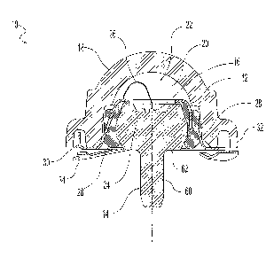
With reference to Figures 1-4, an LED package 10 of a system 100 is shown. The
LED package 10 of the system 100 comprises an annular anode 12, a cathode, 14,
an LED
die 16, and a lens 18. Also, a silicone or viscous material 20 may be located
in a cavity 22
defined by the annular anode 12, the cathode 14, and the lens 18. This viscous
material 20
may be a clear silicone gel or grease, a non-resilient material, a non-liquid
material, or the
like. In other embodiments, the cavity 22 may contain a liquid, resilient or
solid material
or may not contain any material.
The LED die 16 is coupled to a die cup 24 of the cathode 14 and to the anode
12 via
wire bonding 26. The LED die 16 may be coupled by a thermally and electrically
conductive epoxy or the like to the die cup 24. The die cup 24 may have
reflective
surfaces. The cathode 14 is coupled to the anode 12 through use of a coupling
material 28,
which may be liquid crystal polymer, or the like, so long as the material is
thermally
conductive and electrically insulating. After dispensing the viscous material
20 into the
cavity 22, the lens 18 is coupled to the anode 12 via complementary coupling
devices 30
(see Figure 3), which may be barbs or anode retention tabs, and coupling
devices 31 (see
Figure 3), which may be receiving openings. The lens 18 further comprises
protrusions 32,
which may be lens feet, that allow the LED package 10 to be removeably secured
in a
6
CA 02438889 2003-08-20
WO 02/069409 PCT/US02/04643
coupling device 36 of the mounting device 54 in a socket like fashion, where
the feet 32
are biased against the coupling device 36 via flexible extensions 34 extending
from a
peripheral portion of the anode 12. Alternatively, as seen in Figures 9-10,
the socket
device may be incorporated directly in a light fixture to eliminate the need
for secondary
coupling devices and printed circuit boards. After being removeably secured in
the
mounting device 54, extensions 55 extending from the mounting device 54 are
received in
openings 56 in a printed circuit board (PCB) 40 and extension 57 extending
from the
mounting device 54 is received in opening 58 in the PCB 40 to couple the
mounting device
54 to the PCB 40. Within the mounting device 54, an opening 59 receives the
cathode post
60.
The annular anode 12 is central to the system 100. The annular anode 12 is a
lead
frame for the LED system 100. As best seen in Figure 4, in the circular
embodiment
shown, the annular lead frame 12 somewhat resembles an inverted pie pan having
a
centralized, preferably concentric window 50 formed in the "bottom" 52
providing access
to the LED die 16 and wire bonding 26, and through which light emitted from
the LED die
16 is distributed to the lens 18. However, other embodiments contemplate other
generally
symmetrical shapes, which are equally well suited as lead frames, as is the
annular
embodiment. As discussed above, in an embodiment the stamped barbs 30 are
formed
about the periphery of a body of the lead frame 12 for captive engagement
between the
lead frame 12 and the receiving openings 31 of the lens 18 during assembly of
the LED
package 10.
The LED package 10 also allows for significant improvement in the product
assembly process. Since the circular LED package 10 is not orientation-
specific, it may be
mounted in the mounting device 54 on the PCB 40, or as seen in Figure 10 the
LED
package 10 may be mounted in mounting device 254 in a light illumination
device 200, or
as seen in Figure 11 the LED package 10 may be mounted in a mounting device
354 in an
light fixture assembly 300, where in any of these embodiments the LED package
10 is
mounted in any orientation, radially about its center. This eliminates the
need for specific
component orientation prior to assembly. The embodiment shown in Figures 1-5
may
resemble an RCA-type plug that allows the LED package 10 to be easily
installed into the
7
CA 02438889 2003-08-20
WO 02/069409 PCT/US02/04643
coupling device 36 in the mounting device 54 in a socket like fashion without
the need for
heat or any specialized tools.
The annular form of the lead frame 12 is further designed to provide a large
surface
area for sinking heat generated during use. The shape has the still further
benefit of
reducing thermal expansion due to hoop stresses inherent with the annular
geometry.
Other embodiments of the LED package 10 utilize multiple LED dies 16, such as
the embodiment shown in Figure 7, which may include a red, green, and blue LED
die 16.
In some of these embodiments, each of the LED dies 16 must be coupled via the
wire
bonding 26 to different segments of the lead frame 12 to provide a separate
anode segment
12A-C for each LED die 16. With the annular configuration of the embodiments,
multiple
wire bonding 26 from the lead frame 12 to the multiple LED dies 16 can be
easily
accommodated.
Finally, the lead frame 12 may be laser welded, rather than soldered, or
otherwise
mechanically coupled to the PCB 40 to provide electrical contact between the
LED
package 10 and the PCB 40, thereby minimizing the risk of overheating the LED
die 16
during assembly of the LED package 10 into a product or subassembly.
The LED package 10 utilizes a lens 18, which may be premolded and may be
constructed of any one of a number of known materials, which may be epoxy
resin, urea
resin, silicon resin, acrylic resin, glass, or the like, in various lens
patterns or geometries.
While shown in a circular embodiment, the shape of the lens 18 may be any
generally
symmetrical shape such as, without limitation, square, hexagonal, triangular
and the like.
The lens 18 provides the optical pattern for the LED package 10, and may be
configured as
a convex, concave, or collimating lens and may be optically clear or contain
dispersants to
diffuse the outputted light. In several embodiments, the inside surface of the
lens 18 may
be coated with a suitable light excitable material or the lens 18 may comprise
a suitable
light excitable material, which may be a phosphor material, for generating
white light when
excited with a blue, ultraviolet, or other color LED die 16. In other
embodiments, the
silicone or viscous material 20 may comprise the light excitable material. In
addition, the
lens 18 both partially defines the cavity 22 for the viscous material 20 and
acts as a
protective shield for the LED die 16 and attendant wire bonding 26. By
premolding the
8
CA 02438889 2003-08-20
WO 02/069409 PCT/US02/04643
lens 18, the optical output of the LED package 10 is easily modified by
producing a
different configuration, pattern, or geometry of the lens 18.
The viscous material 20 may be an optical quality gel or grease or other
viscous
material, which may have a refractive index of n ~ 1.70 or greater. The
viscous material 20
is contained in the lens 18 to possibly provide gradual transition of index of
refraction
between the LED die 16, which may have an index of refraction about n ~ 3.40,
and the
lens 18, which may be have an index of refraction of about n ~ 1.5. If the
viscous material
20 is an optical gel it may be of the type manufactured by Nye Optical. In
addition, the
viscous material 20 reduces the stress on the wire bond 26 and LED die 16
caused by
thermal expansion. In one embodiment, the viscous material 20 is formed so
that it has
varying indexes of refraction by arranging it in layers within the lens 18,
where the layer
having the highest index of refraction is closest to the LED die 16. In
addition to
facilitating assembly of the LED package 10, the varying layers of viscous
material 20
between the LED die 16 and the lens 18 also lessens the Fresnel losses within
the LED
package 10.
As previously discussed, in some embodiments a white emitted or output light
is
produced using a blue, ultraviolet, or other color LED die 16 by exciting
light excitable
materials, which may be fluorescent materials, that may be located in or on
the lens 18, or
similar to what is disclosed in Shimizu et al. in U.S. Pat. Nos. 5,998,925 and
6,069,440, the
viscous material 20 may contain a suitable phosphor material. However, unlike
the
Shimizu et al. patents, in some embodiments one or more layers of the viscous
material 20
replaces the prior art cured epoxy coating resin. In addition, in other
embodiments, rather
than being confined to the cavity 22 holding the LED die 16, the phosphor
bearing viscous
material 20 fills the cavity 22 of the entire lens 18, which is more effective
for converting
more of the excitation output into white light. In the circular embodiment
shown in the
figures, the semispherical configuration of the phosphor bearing viscous
material 20 also
provides more of an omni-directional output than the LEDs generally depicted
by Shimizu
et al.
The wire bonding 26 used to connect the lead frame 12 to the LED die 16 may be
gold, but may also be made from copper, platinum, aluminum or alloys thereof.
The
diameter of the wire bonding 26 is typically in the area from 10-45 pm. As
recognized in
9
CA 02438889 2003-08-20
WO 02/069409 PCT/US02/04643
the art, because of thermal expansion coefficients between materials in LEDs
made
according to the prior art methods, wire bonds with diameters less than 25 pm
are not
recommended because of breakage at the bonding point. Accordingly, unlike the
prior art,
the wire bonding 26 is encapsulated in a viscous material rather than a hard
resin, thus
permitting some expansion without loss of the electrical bonding. The wire
bonding 26 is
connected to the electrodes) of the LED dies(s) 16 and the lead frame 12 by
normal wire
bonding techniques.
The cathode 14, which may be a copper slug or heat sink, is provided at the
center
of the LED package 10, and serves as the cathode for the LED package 10. As
discussed
above, the cathode 14 is configured to have the die cup 24 at its uppermost
surface, within
which the LED die 16 is mounted. As also discussed above, the liquid crystal
polymer 28
may be used to couple the cathode 14 into place within the anode 12. The
liquid crystal
polymer 28 also provides a barrier to seal the viscous material 20 in place.
In addition,
because the liquid crystal polymer 28 is thermally coupled to the anode 12 it
provides for
additional heat sinking for the LED die 16. The inner surface of the die cup
24 may be
finished with a reflective surface, via plating or other means, in order to
direct the light
emitted from the LED die 16 in a predetermined manner. The mass of the cathode
14
provides superior heat sinking for the LED die 16 to allow higher power to be
applied to
the LED die 16, resulting in higher lumen output.
In some embodiments, the cathode 14 may be provided with an integral center
post
60. When so configured, the LED package 10 can be assembled into a PCB 40
assembly
by normal soldering techniques or, without the use of heat, by press fitting
the LED
package 10 into a complementary socket arrangement of mounting devices 32 and
36. In
other embodiments, a base 62 of the cathode 14, when there is no integral
center post, can
be laser welded or otherwise mechanically coupled to the anode 12 to provide
electrical
contact. In other embodiments, as seen in Figure 6, each of the cathodes 14 of
each of the
LED packages 10 may be connected to receiving devices 72 on a carrier strip
42, where
each of the anodes 12 may be connected using an carrier strip 70. In other
embodiments,
as seen in Figures 8A-B, an LED package 410 comprises a cathode 414 with a
post 460
that comprises protrusions 470 that may be coupled to a complementary coupling
device in
the system, which may a bayonet type coupling system. In other embodiments, as
seen in
CA 02438889 2003-08-20
WO 02/069409 PCT/US02/04643
Figures 9A-B, an LED package 510 comprises a cathode 514 with a post 560
having a
threaded outer surface 570, which may be coupled to a complementary coupling
device in
the system.
The LED die 16, which may have an index of refraction of n ~ 3.40, provides
lumen output. The LED die 16 design and its method of manufacture are
described in by
Shimizu and others. The LED die 16 may be a multi-layer epitaxial
semiconductor
structure whose anode and cathode are electrically mounted to an inner lead 12
and mount
lead 14, respectively. When energized, the LED die 16 is the component that
emits light of
a wavelength predetermined by its chemical makeup. As discussed above, to
produce the
desirable white LED output, multiple colors of LED dies 16, such as red, blue,
and green,
may be combined into a single LED package, as seen in Figure 7. However, in
other
embodiments a blue, ultraviolet, or other color LED die 16 is used to excite a
phosphor
containing component in the lens 18 or silicone or viscous material 22 in
order to produce a
white light. Some prior art devices that have similar functions are Singer et
al. that teaches
the use of a phosphor layer on top of a blue LED chip to produce a white LED,
Shimizu et
al. that teaches the use of phosphor materials embedded into a resin coating
material place
over the LED chip, and Shimizu et al. that teaches the use of phosphor
materials in the
molded lens surrounding the LED chip.
As seen in Figure 6, one embodiment provides an array of the anodes 12 that is
formed continuously into the carrier strip 70, which may be an anode Garner
strip, maybe
by stamping or other conventional means. This configuration facilitates
manufacturing of
the LED package 10. The anode carrier strip 70 also provides for alternate
means of
packaging the LED package 10 into subassemblies. For example, the carrier
strip 42,
which may be a cathode carrier strip, containing receiving devices 72 having a
common
cathode may be employed as one assembly. In such an application, only one
electrical
connection to the cathode would be necessary. Likewise, the anode carrier
strip 70 can be
configured to have a common anode, in which case an entire strip of the LED
packages 10
can be easily assembled into a product by making only two electrical
connections. The
cathode carrier strip 42 and the anode carrier strip 70 may be periodically
scored (shown as
dashed lines) along their length to enable the cathode carrier strip 42 and
the anode Garner
strip 70 to be in broken into predetermined lengths.
11
CA 02438889 2003-08-20
WO 02/069409 PCT/US02/04643
The various embodiments have been described in detail with respect to specific
embodiments thereof, but it will be apparent that numerous variations and
modifications
are possible without departing from the spirit and scope of the embodiments as
defined by
the following claims.
12