Note: Descriptions are shown in the official language in which they were submitted.
CA 02439233 2003-08-22
WO 02/065165 PCT/USO1/20033
COMPENSATION AND/OR VARIATION OF WAFER LEVEL
PRODUCED LENSES AND RESULTANT STRUCTURES
BACKGROUND OF THE INVENTION
Field of the Invention
The present invention is directed to making lenses on a wafer level, in
particular to using wafer processing techniques to create a desired lens
functioning,
illustratively starting with substantially identical base lenses formed on a
wafer level,
and structures formed thereby: v
Description of Related Art
Previous wafer level manufacturing techniques have assumed that the lenses
made on the wafer level were identical within required parameters for their
end use.
As tighter tolerances are required, this assumption may no longer be
realistic. As the
use of arrays of micro-optical lenses becomes more prevalent, differences
between
lenses therein may result in erroneous functioning. Further, many applications
are
now requiring the use of microlens arrays in which the microlenses therein
have
different properties, e.g., different focal lengths. Typically, such different
arrays were
created using different parameters for the underlying lenses themselves.
However, it
is easier to create a wafer of substantially identical microlenses than to try
to adjust
the parameters for individual microlenses thereon.
This creation of an array of different lenses is particularly difficult when
the
microlenses are to be refractive lenses created using reflow techniques. When
etching
reflowed lenses into a substrate, lenses having different radii of curvature
require the
chemistry used during etching to be altered at different points. Thus, the
creation of
an array of different reflowed refractive lenses on a wafer level becomes
impractical.
SUMMARY OF THE INVENTION
The present invention is therefore directed to methods and structures which
overcome at least one of the above disadvantages.
-1-
CA 02439233 2003-08-22
WO 02/065165 PCT/USO1/20033
It is an object of the present invention to compensate andlor vary optical
characteristics of an optical lens structure based on a substantially
identical refractive
surfaces created on the wafer level.
It is another object of the present invention to correct for variations in a
refractive surfaces created on a wafer level from a desired functioning.
It is another object of the present invention to create an array of microlens
structures having different optical characteristics based on an array of
substantially
identical refractive surfaces created on the wafer level.
At least one of the above and other objects may be realized by providing an
array of
micro-optical components includes at least two micro-optical components. Each
micro-
optical component includes a refractive surface and a corresponding
compensation surface
for the refractive surface. The corresponding compensation surface includes a
corresponding
compensation feature when the refractive surface deviates from a desired
optical
performance. The micro-optical component provides the desired optical
performance. At
least two refractive surfaces of the array of micro-optical components are
formed to have
substantially a same desired optical performance. The array of micro-optical
components
includes at least one corresponding compensation feature, at least two
compensation surfaces
of the array of micro-optical components being different from one another.
All combinations of refractive surfaces and corresponding compensation
surface may operate at a same focal length or different combinations may
operate at
different focal lengths. The refractive surfaces and the corresponding
compensation
surfaces may be formed on a same substrate or on different substrates of at
least two
substrates bonded together. The corresponding compensation features may
correct
for aberrations in a corresponding refractive surface.
The corresponding compensation features may include a corresponding
separation of the corresponding compensation surface from the refractive
surface in
accordance with a desired focal length of the combination of the refractive
surface and
the corresponding compensation surface. The corresponding separations may be
formed in accordance with a measured focal length of a corresponding
refractive
surface.
CA 02439233 2003-08-22
WO 02/065165 PCT/USO1/20033
The desired focal point of the micro-optical component may be on a back
surface of a substrate on which the micro-optical components are formed or on
a
substrate bonded thereto.
The corresponding compensation features may include a diffractive element,
which may correct for aberrations in a corresponding refractive surface.
At least one of the above and other objects may be realized by providing a
method of forming micro-optical components having a desired optical
performance.
This includes creating a plurality of refractive surfaces on a substrate,
providing a
corresponding plurality of compensation surfaces, one for each refractive
surface,
measuring an optical performance of at least one refractive surface of the
refractive
surfaces, comparing measured optical performance with a desired optical
performance, forming a compensation profile on a compensation surface when a
corresponding refractive surface deviates from its desired optical
performance,
creating refractive surface-compensation surface pairs, each pair having its
desired
optical functioning; and
separating the plurality of pairs into a desired number of micro-optical
components.
The separating may create a plurality of pairs or may create at least one
array of
pairs.
The forming of compensation features may include forming compensation
features on the substrate on which the plurality of refractive surfaces have
been
formed. The forming of compensation features may include forming the
compensation
features on a different substrate than the substrate on which the plurality of
refractive
surfaces have been formed, and bonding the substrate having the compensation
features and the substrate having the plurality of refractive surfaces. The
forming of
compensation features may include etching the substrate in accordance with a
desired
focal length of the micro-optical component. The etching may result in
different focal
lengths for at least two of the micro-optical components. The forming of
compensation features includes etching the substrate in accordance with a
measured
focal length of the corresponding refractive surface. The forming of
compensation
features may include etching using a single mask to simultaneous create a
pattern for
all of the compensation features. The forming of compensation features may
include
-3-
CA 02439233 2003-08-22
WO 02/065165 PCT/USO1/20033
etching using a single mask to create a pattern for the compensation features,
the
single mask being moved to create the pattern for the compensation features.
The
forming of compensation features may include forming a diffractive element.
The
forming of compensation features may include creating at least two
corresponding
compensation features for different compensation surfaces that are different
from one
another.
A desired focal point of the micro-optical components may be on a back
surface of a substrate on which said at least two refractive surfaces are
formed or on a
substrate bonded thereto.
The creating of the plurality of refractive surfaces may include using the
same
process for all of the refractive surfaces.
The measuring of optical performance may include measuring optical
performance for each refractive. The measuring of optical performance may
include
measuring optical performance for a subset of the plurality of refractive
surfaces.
These and other objects of the present invention will become more readily
apparent
from the detailed description given hereinafter. However, it should be
understood that the
detailed description and specific examples, while indicating the preferred
embodiments of the
invention, are given by way of illustration only, since various changes and
modifications
within the spirit and scope of the invention will become apparent to those
skilled in the art
from this detailed description.
BRIEF DESCRIPTION OF THE DRAWINGS
The foregoing and other objects, aspects and advantages will be described with
reference to the drawings, in which:
FIG. 1 is a schematic side view of a microlens system in accordance with an
embodiment of the present invention;
FIG. 2 is a schematic side view of a microlens system on a substrate in
accordance with an embodiment of the present invention;
FIG. 3 is a schematic side view of a microlens system on a substrate in
accordance with an embodiment of the present invention;
-4-
CA 02439233 2003-08-22
WO 02/065165 PCT/USO1/20033
FIG. 4 is a schematic side view of a microlenssystem on a substrate
in
accordance with an embodiment of the present
invention;
FIG. 5 is a schematic side view of a microlenssystem on a substrate
in
accordance with an embodiment of the present
invention;
FIG. 6 is a schematic side view of a microlenssystem on a substrate
in
accordance with an embodiment of the present
invention;
FIG. 7 is a schematic side view of a microlenssystem on a substrate
in
accordance with an embodiment of the present
invention; and
FIG. 8 is a schematic side view of a microlenssystem on a substrate
in
accordance with an embodiment of the present
invention.
DETAILED DESCRIPTION OF THE EMBODIMENTS
In the following description, for purposes of explanation and not limitation,
specific details are set forth in order to provide a thorough understanding of
the
present invention. However, it will be apparent to one skilled in the art that
the present
invention may be practiced in other embodiments that depart from these
specific
details. In other instances, detailed descriptions of well-known devices and
methods
are omitted so as not to obscure the description of the present invention with
unnecessary details.
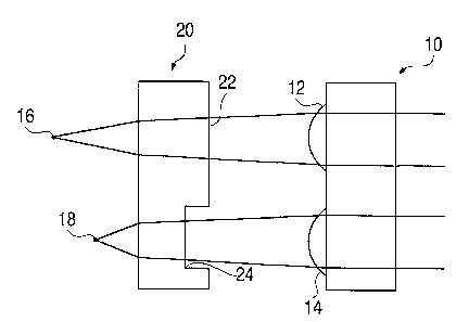
Figure 1 illustrates a lens array 10, here shown with two lenses 12, 14, which
are substantially identical to one another. In a desired application, these
two lenses
12, 14 are to have different focal lengths. Such applications may include
using the
lens array 10 to collimate or focus two or more sources 16, 18 provided at
different
distances from the lens array. By providing a thickness compensator 20, here
shown
as an etched spacer wafer presenting a first thickness 22 and a second
thickness 24,
the resulting optical path length is the same for both lenses. Thus, while the
lenses 12,
14 are the same and the sources 16, 18 corresponding thereto are at different
positions,
the output of the resultant lens structure of the lenses 12, 14 and
corresponding
thicknesses 22, 24 is the same.
When it is assumed that the substantially similar lenses 12, 14 are within the
required tolerances for the desired application, the thickness compensator 20
may be a
-s-
CA 02439233 2003-08-22
WO 02/065165 PCT/USO1/20033
spacer wafer having various etch depths 22, 24 therein, which may be formed
using a
mask. Not every refractive surface may require the thickness compensator 20 to
be
etched, e.g., when the thickness provided by the compensator 20 alone is
appropriate.
Since the desired focal lengths are known, the pattern for the different etch
depths
may be provided on a mask which is then transferred to a substrate, bonded to
the
wafer of micro-optics, with the resultant structure providing the desired
focal length to
the corresponding sources. While the configuration shown in Figure 1 is
especially
advantageous when the microlens system is to replace a graded index (GRIN)
lens,
since a flat surface at the interface will be provided, the thickness
compensator may
also be etched on an opposite face of the refractive lenses, with the
orientation of the
resultant structure depending upon the end use.
If parameters in addition to or other than focal length are to be altered,
other
optical elements may be provided in the system rather than or along with the
spacer
elements 22, 24. Rather than a thickness compensator 20, a profile compensator
30 is
provided, as shown in Figure 2. For example, diffractive elements 32, 34 may
vary
the focal lengths, other parameters, and/or correct for aberrations, e.g.,
variations in
the conic constant, in the array. These diffractive elements 32, 34 may be
different
from one another. Further, not all refractive surfaces in the array 10 may
required any
compensation features. The corresponding compensation surface of the
compensator
30 for these refractive surfaces would then be left blank.
When the parameters of the lens system itself are not to be varied, but are
rather to be maintained within a certain tolerance level for a desired
application,
deviations from the desired output may be compensated for in a similar
fashion. In
other words, the above compsenators may be used to correct for variations in
the
fabrication process. For example, as shown in Figure 3, if variations in the
fabrication
process result in microlenses 42-48 on a wafer 42 deviating from a desired
focal
length outside the tolerances for the end use, a thickness compensator 50 with
various
etch depths 52-58 can be used to compensate for the variations in the focal
lengths for
the corresponding microlenses to within the desired tolerances. As can be seen
in
Figure 3, the microlens components (42, 52), (44, 54), (46, 56), (48, 58)
focus/collimate to/from detectors/sources 62-68 from the same input plane to
the same
-6-
CA 02439233 2003-08-22
WO 02/065165 PCT/USO1/20033
output plane. While the microlenses 42-48 are shown in Figure 3 functioning as
an
array, once bonded with the wafer 50 containing the varying etch depths, this
resultant
structure may also be diced to form any desired array of microlens components
or
individual microlens components.
When the end structure is to be an array of microlens components and a flat
surface for coupling is not needed, the etch depths may be provide on an
opposite
surface of the substrate, as shown, for example in Figures 4 - 8. This
configuration is
particularly useful when all of the sources or devices to be coupled to 62-68
are set to
a fixed distance. In Figures 4-6, the two substrates 50, 40 are shown bonded
together
by bonding material 70. Figures 7 and 8 illustrate a single substrate
configuration.
In addition to or instead of correcting for focal lengths, additional optical
elements, shown in Figure 5 as diffractive elements, may be incorporated to
correct
for focal lengths or other errors in the refractive surfaces.
When the wafer 40 is to be diced to form individual microlens components, the
individual etch depths may be created to provide the focus at the surface of
the
substrate. The configuration is useful when no air gaps should be introduced
into a
system, e.g., when coupling to or from a fiber. Rather than adjusting the
apparent
focal lengths of the microlens components, the substrate is etched so that the
focus of
the corresponding refractive surface is incident thereon. In contrast to the
previous
embodiments, the focal lengths of the refractive surfaces are not corrected to
be a
desired focal length, but rather the corresponding thickness of the substrate
80 is set to
the actual focal length of the refractive surfaces, as shown in Figure 6.
While the above embodiments have employed two substrates, one substrate
with the microlenses thereon and the other substrate having compensators
thereon, if a
single surface is sufficient to provide the desired result, then the structure
may be
formed on a single substrate 100, as shown in Figures 7 and 8, with the
refractive
surfaces 42-48 on one side, and the compensation features 102-108 or 110-116
on the
other. Having a single substrate reduces positioning errors.
When the refractive surfaces are to be corrected, a variety of manufacturing
techniques may be employed. When the refractive surfaces have sufficiently
similar
deviations from a desired parameter, the same structure may be provided for
all
CA 02439233 2003-08-22
WO 02/065165 PCT/USO1/20033
refractive surfaces. If the refractive surfaces are predictably off each time
they are
generated in accordance with their respective position on the substrate, a
mask may be
created to form the compensator. If adjacent refractive surfaces suffer from
similar
errors, one refractive surface may be measured and the same compensator may be
provided for appropriate refractive surfaces. For situations where there are a
fixed
number of variations across the array, e.g., five, one of these different
patterns may be
provided where appropriate. In the most comprehensive compensation, the
parameters
of interest for each refractive surfaces are measured, with a compensator
being created
for each refractive surfaces on the measurement.
When compensating for measured refractive surface variations from a desired
focal length, instead of creating a mask for each wafer, a stepper can be used
to create
the desired etch depths. For example, the refractive surfaces may be created
on the
first side of a substrate in a conventional manner, e.g., using reflow or gray
scale
lithography. The focal length of each refractive surface is then measured. On
the
other side of the substrate opposite the refractive surface, the substrate may
be etched
to provide an appropriate thickness such that the combination of the
refractive
surfaces and its corresponding substrate thickness provide a desired focal
length.
Rather than creating a mask for the etching, the stepper of the lithographic
equipment
and a mask with a single rectangular or square opening can be used. For
example, if
the lens diameter, or useful area, is 300 microns, a 300microns by 300 micron
square
opening can be used for the mask. This opening is stepped across the wafer one
lens
at a time, only certain portions corresponding to certain refractive surfaces
are
exposed in accordance with the measured focal lengths. After exposure, the
second
side of the substrate is selectively etched. This process may be repeated N
times to
achieve up to 2N different levels of etch depth. Such etching is set forth,
for example,
in U.S. Patent Re 36352 to Swanson et al. Alternatively, the mask may be
stepped
and exposed with different exposure energies to get an essentially arbitrary
number of
distinct levels. After such varying exposure energies, the entire wafer could
be etched
one time to achieve the different etch depths corresponding to the exposure
energy.
Any other transfer process, e.g., laser direct write, which varies etch depth
with
exposure, may be used.
_g_
CA 02439233 2003-08-22
WO 02/065165 PCT/USO1/20033
Of course, the use of the compensator to both adjust the focal lengths across
the
array to be different from one another and to improve any errors arising from
the
processing may both be incorporated in determining the required compensation.
Further, the material in which the etch depths are formed may be of a higher
refractive
index than the refractive microlenses, so that variations in thickness will
have a more
significant impact on the focal length of the combination. This material may
be a
different substrate material or may be a layer of material provided on a
substrate in
which the varying etch depths are formed. Alternatively, rather than etching,
selective
deposition of material may be sued to form the compensation features.
It will be obvious that the invention may be varied in a plurality of ways.
Such
variations are not to be regarded as a departure from the scope of the
invention. All
such modifications as would be obvious to one skilled in the art are intended
to be
included within the scope of the appended claims.
-9-