Note: Descriptions are shown in the official language in which they were submitted.
CA 02441447 2003-09-18
METHOD AND APPARATUS FOR ELECTRICAL COMMONINO
OF CIRCUITS
Field of the Invention
This invention relates to electrical testing of electronic circuits and in
particular improved
methods and apparatus for testing electronic circuits such as those existing
in chip carriers,
printed circuit boards, substrates and other microcircuit devices.
D~ckground of the Invention
Flaws resulting in manufacturing processes of microcircuit devices can create
undesired
electrical conditions in electrical circuits contained within such devices
resulting in flawed or
inoperable electrical circuits wherein the flawed circuits do not function as
originally intended
and designed. In order to verify the electrical integrity of electronic
circuits such as those present
in chip carriers, printed circuit boards, electronic substrates or other
microcircuit devices, during
manufacture of such devices such circuits are typically submitted to
electrical testing in an effort
to detect unintended design flaws such as conditions of electrical shoats or
opens in the circuits.
There is a significant ongoing design and manufacturing effort ~~ithin the
electronics industry to
create physically smaller and more compact electronic components and
substrates. When
attempting to make smaller substrates, the density of the electronic circuits
on the substrates
increases and it is a requirement that the pads on the substrates be placed
much closer together
compared to substrates using less dense electronic circuits. With increases in
electronic circuitry
density the contact pads, which represent extremities of the circuits are
spaced ever-closer
together, especially in the region of the substrate where relatively smaller
chips or components
are to be subsequently connected. This causes difficulties in effecting
contact of the desired
individual circuit contact pads on the surface of the substrate ivor purposes
of detecting undesired
electrical conditions in the individual circuits.
Typical substrates, for example, chip carriers, printed circuit boards,
electronic substrates, or
similar devices, comprise electronic circuits and the substrates physically
and spatially support
CA9-2003-0004 1
CA 02441447 2003-09-18
the electronic circuits. A substrate comprises non-conductive material so that
it does not interfere
with the normal operation of the electrical circuits supported thereon. These
arrangements are
well known in the art. The substrate typically includes electronic circuits
and a first group of
pads located on one surface of the substrate, with the pads electrically
connected to ane or more
of the electronic circuits. The pads are used to connect the electronic
circuits to a first electronic
device, for example, an electronic chip. A second group of pads located on
another surface of
the substrate, are electrically connected to the electronic circlets and
intended to connect the
electronic circuits to a second electronic device, for example, a printed
circuit board. The
electronic circuits form a plurality of predetermined conductive pathways
between the first and
second groups of pads on the substrate.
A known approach used for testing and detecting undesired electrical
conditions such as open
circuits, where contact pads are relatively closely spaced is referred to as
electrical-communing.
With this approach, all the contact pads of one group of pads which represent
all the first
extremities of the electronic circaits of the substrate are electrically
shorted. The electronic
circuits are all thus effectively shorted and connected together. Test probe
devices are contacted
to the second group of pads which represent the other extremities of the
electronic circuits and
which pads are typically spaced further apart from each other than those pads
at the first
extremities of the circuits. The test probes are connected to a test mechanism
for testing the
electronic circuits for adverse electrical conditions and verify whether the
electronic circuits
exhibit any adverse electrical conditions. Electrical continuity-testing of
electrical circuits may be
carried out with the use of, for example: an ohm meter, a voltmeter, an
ammeter, or equivalent,
in order to verify the electrical iaotegrity of electronic circuits by
detecting undesired electrical
conditions in the circuitry, as is well known in the industry.
Problems exist resulting from the use of known electrical-communing methods
and apparatus for
detecting undesired electrical condition of electronic circuits on substrates
which could produce
'false open' results. These problems include:
~ the electrical-communing mechanism does not making suitable contact with the
contact
pads;
CA9-2003-0004 2
CA 02441447 2003-09-18
~ the pads are contaminated, for example, by a non-conductive substance on the
pads which
substantially prevents electrical contact being made between the pads and the
electrical-communing mechanism;
~ one or more pads may be deformed, thus creating a condition where the pad
does not
make contact with the electrical-communing mechanism;
~ the electrical-communing means is not sufficiently locally compliant with
the pads
resulting in ineffective electrical contact;
~ the electrical-communing mechanism does not have a capability to overcome
aspects of
'self damage' that may be reflected in the contacts so that a reliable
communing of the contact
pads can be effected, for example, the self damage being caused by
contaminants, or the pads
having surface inconsistencies, or the electrical-communing mechanism having
surface
inconsistencies; and
~ the electrical-communing means may deposit ara unwanted residual
electrically
non-conductive material on the surface of the pads and the substrate, such
that it may be difficult
to remove the residual material from the pads and the substrate after testing
is performed.
Known prior art attempts to solve the above and other problems associated with
electrical-communing approaches presently used include the use of a flexible
sheet, for example,
a conductive polymeric sheet or metallized polymeric sheet as described in US
patent 5,898,311
issued April 27, 1999, entitled Shorting Pad Having A Flexible Conductive
Sheet and US patent
5,900,316 issued May 4, 1999, entitled Flexible Conductive Sheet, both of
which are assigned to
International Business Machines Corporation. However. diff'zculties may arise
with the use of
such polymeric sheets in that:
~ the sheet may leave a residual contamination on the surface of the pads and
substrate
during the test which may be difficult to remove;
~ the sheet has a capability of being susceptible to phy°sical damage
when contacting the
pads;
~ the sheet requires relatively large contact forces to ensure that the
polymeric sheet makes
sufficient contact with all of the pads and the large forces may result in
damage to the substrate
and any test fixture; and
CA9-2003-0004 3
CA 02441447 2003-09-18
~ the sheet may be insufficient to completely prevent 'false opens' because
the polymeric
sheet does not have sufficient capability for being substantially and
completely locally compliant
with the contact pads.
From the above description, it should be appreciated that there is a need for
improvements in the
testing of electrical circuits that are manufactured on substrates and in
particular a need for a
new approach to temporarily electrically common or short such circuits. A
novel and unobvious
solution is needed to provide an electrical-commoning anechanism that
overcomes the
aforementioned problems inherent in the prior art.
Summary of the Invention
Therefore, an impoa-tant objective for manufacturers of substrates is their
constant desire to find
and detect circuits which are flawed and which contain undesired electrical
conditions, to
thereby reduce manufacturing waste, reduce customer complaints, and the like.
The present invention provides a method and apparatus for electrically
commoning the
electronic circuits supported by a substrate, and to effectively and cost
efficiently in a timely
manner to determine the existence of undesired electrical conditions
associated with the
electronic circuits to thereby reduce costs associated with manufacturing
waste and customer
complaints. Flaws in manufacturing processes which may have caused an
occurrence of
undesired electrical conditions in the electrical circuits thereby creating
flawed electrical circuits
not being able to function as expected or desired can be effectively detected
at an appropriate
early stage of the assembling process.
The present invention provides a method and apparatus for testing the
continuity of electronic
circuits and to accommodate requirements to make even smaller electronic
devices in attempts to
physically decrease the size of substrates thereby increasing the density of
the electronic circuits
and subsequently placing the pads much closer together compared t;o electronic
circuits used in
less dense circuits.
CA9-2003-0004 4
CA 02441447 2003-09-18
According to one aspect of the present invention, there is proaeided an
apparatus for use with a
substrate supporting a plurality of contact pads for electrically communing
the contact pads. The
apparatus comprises a container for confining a quantity of electrically
conductive particles and
having said substrate positioned within said container having a first group of
a plurality of
contact pads on a first surface thereof in contact with said particles. At
least same of said
electrically conductive particles contact other of said particles and said
contact pads of said first
group of contact pads on said surface of said substrate and means to maintain
said particles in
contact with the surface of said substrate and said contact pads whereby said
contact pads are
electrically communed.
According to another aspect of the present invention, there is provided a
method for electrically
communing contact pads located on a first surface of a substrate wherein each
pad is connected
to a circuit supported by said substrate. The method comprises the steps of
providing a
container for confining electrically conductive particles and providing a
supply of electrically
conductive particles in said container. A substrate having a first group of a
plurality of contact
pads on one surface thereof is placed and held in said container such that the
pads contact said
particles and the particles are maintained in contact with other of said
particles and said pads
whereby said pads are electrically communed.
Description of the Drawings
The above and other objectives of the subject invention will be better
understood with reference
to the drawings in which:
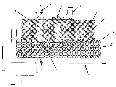
Figure 1 shows a cross section drawing of a testing apparatus embodiment of
the present
invention.
Figure 2 shows the drawing of Figure 1 incorporating a substrate having
recessed pads.
Figure 3 shows a cross-sectional drawing of another embodiment of the testing
apparatus
accommodating a substrate positianed on flexible walls of a container.
Detailed Description of the Preferred Embodiments of the invention
The term 'electrically communing' of contact pads or electronic circuits as
used in this disclosure
has the same meaning as electrically shorting of pads or circuits, as is well
known in the art.
CA9-2003-0004 5
CA 02441447 2003-09-18
An overview of aspects and advantages of the subject invention to effect the
described electrical
commoning of circuitry and to carry out electrical testing of circuitry while
eliminating known
problems of the prior art, will first be described followed by a more detailed
description with
reference to the drawings.
The disclosed invention incorporates the use of small electrically conductive
particles, preferably
but not limited to spheres, placed in a receptacle so as to somewhat limit the
horizontal
spreading of the particles. A suitable quantity of the particles for the
container or receptacle can
IO be determined to ensure that the surface of a substrate containing a group
of electrical contacts
or pads to be shorted will always come into contact with a minimum
concentration of particles.
The walls of the receptacle are made from suitable material that may be
flexible, resilient or
compliant, such as compressible rubber, with dimensions designed to ensure
adequate
compaction of the particles within the receptacle to allow the group of
electrical contacts or pads
to meet and be in physical and electrical contact with the contained
particles. As such the
particles simultaneously contact both themselves and the group of electrical
contacts which are
connected to the electrical circuits supported by the substrate to be tested.
The conductive particles are of dimensions which are sufficiently smaller than
the dimensions of
the contact pads such that numerous particles can individually and
simultaneously contact each
contact pad, but large enough to avoid the risk of adhering or becoming
attached to the contact
pads or substrate surface. The exterior of the particles comprise electrically
conductive and
non-oxidizing material such as but not limited to gold or platinum. One means
to effect such a
coating on the particles is by the use of a suitable electrolyses plating
bath. The exterior surface
of each conductive particle is sufficiently rigid to prevent excessive
deformation or
agglomeration of the particles, thus maintaining the original ability of the
particles to be
moveable and to contact themselves and the pads. In one embodiment of the
invention, the core
material of the metal particles is magnetic in nature such that the particles
can be moved by the
use of an external alternating magnetic field. In another embodiment, where
the particles can be
CA9-2003-0004 6
CA 02441447 2003-09-18
moved by ultrasonic means, the core of each particle ynay be made of magnetic
or non-magnetic
material.
As may be appropriate after testing, the substrate surface may be subjected to
a cleaning
operation by blowing inert gas across the surface of the substrate to remove
any residually
adhering conductive particles.
Having the size of the particles somewhat smaller than the dimension of the
contact pads ensures
that the loosely compacted particles, when retained in the receptacle of the
apparatus, acts in a
quasi-fluid nature. The overall surface formed by the particles within the
container/receptacle, is
thus compliant and readily changes shape to accommodate the shapes and
positions of the
contact pads supported by a substrate. In this way the bed of particles
effectively acts to
electrically common or short the contact pads. Numerous advantages follow from
this
arrangement.
If a portion of a surface of a contact pad is covered by a non-conductive
material as by
contamination or by design, the remaining conductive portion of the contact
pad will still be
contacted by some of the particles to ensure meaningful test results. In
addition, with the use of
particles of such small size the physical requirements and constraints
resulting from greater
density of contact pads on a surface of a substrate and decreasing contact pad
pitch/size will be
accommodated for the tesing of the connected circuitry.
This adaptability of the particle bed allows for effective contacting of
contact pads which may be
located somewhat lower than the overall substrate surface. This is the case,
for example, with
printed circuit boards which may contain a non-conductive solder mask of
approximately 20-30
microns thickness on their surfaces with openings, typically approximately 150
microns in
diameter, in the solder mask to reveal the contact pads below the surface
thereof. The contact
pads are therefore effectively 20-30 microns below the surface. The particles,
being significantly
smaller in diameter than the diameter of the openings in the mask and being in
the form of a
CA9-2003-0004 7
CA 02441447 2003-09-18
compliant bed of particles, will effectively enter the openings and make
electrical contact with
the pads.
The quasi-fluid nature of the particle bed in the container is not adversely
affected by or
susceptible to physical damage from any irregular shapes or protrusions from a
hard ceramic
substrate with contact pads. The particle bed can be re-used almost
indefinitely to perform the
testing operation.
The rigid nature of the core component of the electrically conductive
particles prevents
deformation and/or agglomeration of the particles within the container and
maintains the ability
of the particles to contact each other and the pads. The compliant nature of
the particle bed is
maintained and the nature of the particles reduces potential contamination of
the contact pads by
the particles. The non-oxidizing nature of the exterior surface of these
particles ensures
consistent contact between adjacent particles and between the particles and
contact pads. The
combination of the use of these described particles in a container or
receptacle having compliant
walls efficiently provides for the contacting of the pads with the pa~~ticles
using relatively small
forces to achieve the commoning of the pads on a substrate.
Where the core component of the pat-ticles is magnetic in nature a varying
magnetic field may be
used to maintain the particles in constant motion during electrical contact
with the pads and the
subsequent performance of the electrical test. This results in effective
electrical contact of
particles with the pads through constant homogenization of the "particle fluid
bed" while
minimizing the extent to which the particles adhere to themselves and to the
contact pads or to
the substrate itself. Ultrasonic means to place the particles in appropriately
constant motion may
2~ achieve similar advantages and allowing for the particles to be made from a
variety of materials.
With reference to Figure 1 of the drawings, details of a testing apparatus
embodiment 1 of the
present invention will now be described. This embodiment comprises container
or receptacle 10
for confining conductive particles 9 and causing particles 9 to physically
touch other particles
thereby electrically shorting physically touching particles 9. Container 10
and other aspects of
CA9-2003-0004 8
CA 02441447 2003-09-18
this embodiment maintains some shorted particles 9 in physical contact with
pads 6 of a first
group of pads 6 located on a first surface 7 of substrate 3 dvhen a contacting
force generally
shown by arrow 11 is applied on substrate 3 and forceing pads 6 to physically
touch some of the
shorted particles 9. Contacting force 11 may be created and applied by any
appropriate means as
would be known to those having ordinary skill. Since a sufficient quantity of
particles 9 exist in
container 10, pads 6 of the first group of pads on the first surface 7 of
substrate 3 are thereby
substantially electrically commoned or shorted together.
Substrate 3 further comprises circuits 4, such as conductive vias within
substrate 3, which are
connected to pads 6 of the first group of pads 6. Since electronic circuits 4
are connect to pads 6,
circuits 4 are also electrically shorted or commoned by particles 9.
Substrate 3 further comprises a second group of pads 8 :located on another
surface of the
substrate other than surface 7 of substrate 3 as shown. Pads 8 are
electrically connected to the
aforementioned electronic circuits 4 as shown. Substrate 3 physically
separates the second group
of pads 8 from the pads of the f rst group of pads 6 and further prevents the
second group of
pads 8 from physically touching particles 9.
Embodiment of Figure 1 further comprises test device 2 and includes one or
more test probes 5
shown electrically connected thereto and contacted to pads of the second group
of pads 8.
Typically a test probe 5 is connected to each pad 8. Test device 2 is also
electrically connected
to conductive contacting particles 9 contained within container 10. Test
device 2 is thus capable
of detecting the electrical conditions of the electronic circuits 4 connected
to test probes 5 and in
particular any flaw or undesirable electrical condition existing in each
circuit. In practice, test
probe 5 would be moved from one contact pad 8 to another contact pad 8 and
electrical contact
would be made in turn to each of the contact pads 8 in the second group of
contact pads to
thereby in turn assess the electrical condition of each of the circuits 4
connected to pads 8 and
thereby detect any undesirable electrical opens existing in circuits 4.
CA9-2003-0004 9
CA 02441447 2003-09-18
As previously described, particles 9 are electrically conductive thereby
achieving the desired
shorting or commoning relationship when they are in contact with each other
and with pads 6
when located within container 10. In a preferred embodiment, particles 3 are
essentially
spherical in shape and have an exterior surface thereon of a non-oxidizing
material to prevent
formation of electrically insulating oxide on the surface of the particles,
thereby ensuring that
particles 9 are electrically contacted to each other and to pads 6 when
assembled within container
10. Particles 9 may consist of a pore and have an exterior surface coating
formed, for example,
by the use of an electroless plating bath. The inert coating on particles 9
prevent particles 9 from
imparting any contamination to the pads of the first group of pads 6 and
surface 7 of substrate 3.
Various materials could be used for particles 9. The core material could be
any electrically
conductive material, for example, ferro magnetic materials such as iron,
nickel or cobalt. The
core of particles 9 could also consist of suitable non-conductive material
including plastic, with
an exterior coating of electrically conductive material including gold or
platinum. Particles 9
could also be made of all one material such as gold.
As examples of sizes of elements which have been used in association with the
present invention,
a substrate of 1.5 inches square having a chip size of .5 inches square,
include contact pads of
.005 inches in diameter and a pitch or spacing between pads of 150-250
microns. Particles in the
range of 25-30 microns have been found to be practical.
Particles 9 are sufficiently rigid to prevent excessive agglomeration of the
particles thereby
allowing particle 9 to be freely moved within container 10 and to contact pads
6. The
characteristics of particles 9 prevent them from becoming substantially
gathered into a heap or
localized when a contacting force 11 is applied to substrate 3 and thus
particles 9. However on
the other hand particles 9 form a quasi-fluid bed and this bed of particles is
suitably compliant,
flexible or resilient to ensure an extended usable life of the bed of
particles by preventing
individual particles 9 from being subjected to physical damage. Pa.uticles 9
in the bed of particles
as described are capable of being reversibly deformed, wherein a deformation
of the particle bed
allows the bed of particles to resume its original shape thereby preventing
the bed of particles
~CA9-2003-0004 10
CA 02441447 2003-09-18
from becoming permanently misshapen after the contacting force is removed. The
contacting
force may temporarily deform the bed of particles, and after the contacting
force is removed, the
bed of particles resumes its original shape.
The size of particles 9 is selected to ensure accommodation of sufficient
particles for the surface
area of each pad 6. Preferably the particles are sufficiently large so as not
to become wedged in
the space between pads 6 during the testing procedure and small enough so that
more than one
particle contacts the surface of a pad 6. In addition the size and number of
particles 9 in a
particular application are suffident to make electrical contact with pads 9
even when a portion
of pad surface may be covered by a non-conductive material. ~. predetermined
number of
particles can be determined to suitably cover the surface area of pads 6.
In general it has been found useful results are achieved when the diameter of
a spherically shaped
particles 9 is about 1 /3 the diameter of the surface of pad 6. The quantity
of particles 9 to exist in
container 10 for useful results varies on a number of factors including size
of surface 7 of
substrate 3 and configuration of pads 6. It has been found in general that the
thickness of the bed
of particles 9 should be at least as thick as the height of pads 6 above
surface 7.
Container IO has side walls to contain and lunit the horizontal spreading of
particles 9 and to
maintain particles in a predetermined volume of space. The walls of container
10 are preferably
resilient, flexible and compliant to enhance the desire of having some
particles 9 which are
contacting each other when an appropriate force 11 is applied to touch pads 6
of substrate 3. The
walls of container I O are preferably made of suitable flexible material and
are of dimensions so
as to ensure an adequate compression of particles ) when substrate 3 and pads
6 thereon is placed
in container 10 such that pads 6 contact some of particles 9.
Contacting force 11 is applied to substrate 3 to cause susbtrate 3 with pads 6
on surface 7 thereof
to physically contact the particles 9. The contacting force 11 is sufficiently
strong to maintain
pads 6 in stable contact with at least some of particles 9 whereby particles 9
make conforming
contact with pads 6 during application of force 1 I. Force 11 is maintained on
substrate 3 to
CA9-2003-0004 I 1
CA 02441447 2003-09-18
cause pads 6 to contact particles 9 for a sufficient time in order to have the
test performed. The
combination of applied force 11 and the force resulting from the flexibility
of the walls of
receptacle 10 is such as to ensure damage is not imparted to substrate 3 or
contacts 6 by the bed
of particles 9.
Substrate 3 may be connected to other electronic components while the
circuitry 4 supported by
substrate 3 is being tested. As had been described, the first and second
groups of pads on
substrate 3 as shown by references 6 and 8 respectively, may be electrically
connected to an
electronic chip or a printed circuit board, for example.
Tester or test device 2 is used to detect undesired electrical conditions such
as electrical opens
existing in the electronic circuits 4. Test probes S are caused to
sequentially make electrical
contact with pads 8 of substrate 6 during the testing of electronic circuits
4. Test device 2 could
comprise any one or more of an ohm meter, a voltmeter, and an ammeter.
Another aspect of the embodiment of the present invention shown in Figure 1 is
a
motion-inducing mechanism or means (not illustrated in Figure 1 ) for causing
particles 6 to move
toward and touch or make contact with any available surface of pads 6 of
substrate 3 thereby
ensuring particles 6 to be in touch with the surface of pads 6.. Such
mechanism is not shown in
Figure 1. The suitable motion-inducing means could be one of the following
mechanisms or a
combination of any two or more of the mechanisms namely, a shaking-motion
mechanism, a
magnetic-field mechanism, or an ultrasonic mechanism. Such mechanisms for
inducing motion
to the particles are considered to be well known to those of ordinary skill.
~f course for the
magnetic-field mechanism to be effective, particles 9 of magnetic material
would have to be
employed. A shaking-motion mechanism induces a shaking and vibrating motion to
particles 9
thereby causing particles 9 to mo ve toward and make more effective electrical
contact amongst
themselves and with pads 6 of substrate 3. This results from the physical
shaking and vibrating
of particles 9 within container 10. By inducing a shaking motion to particles
9, the particles are
caused to move in a back and forth motion with rapid jerky motions thereby
causing the particles
9 to change their spatial positions to enhance greater contact with pads 6 and
reduce the amount
CA9-2003-0004 12
CA 02441447 2003-09-18
of test time required to effectively test circuitry 4 on substrate 3. An
ultrasonic mechanism may
be coupled to container 10 for causing particles 9 in a similar manner to
shake and vibrate
resulting in more effective electrical contact between particles 9 and pads 6
on substrate 3. The
sound frequencies used may be beyond the range that can be heard by a human
ear. A
magnetic-field mechanism may be coupled to container 10 in which magnetic
particles 9 exist.
The magnetic-field mechanism imparts changing lines of magnetism to particles
9 which
magnetically interact with particles 9 whereby particles 9 become churned so
that freely available
particles 9 make contact with any remaining available spaces on the surfaces
of pads 6. This
enhances the contact of particles 9 with pads 6 and thereby reducing the time
to carry out the
electrical tests on circuitry 4 of substrate 3. The magnetic-field mechanism
may further entail a
degaussing mechanism to remove residual magnetism fiom the particles thereby
preventing the
particles from adhering to pads 6 and to substrate 3. As had been previously
mentioned, the
mechanisms to provide for the shaking-motion, ultrasonic and magnetic field
activity may be
used individually or in any combination in order to enhance the contact of
particles 9 with pads 6
on the surface of substrate 9.
Figure 2 of the drawings illustrates use of the apparatus embodiment of Figure
1 with a substrate
3 in which pads 6 are effectively recessed below the surface of substrate 3.
In practical
situations portions 12 of the surface of substrate 3 upon which contact pads 6
are located, may
be covered by a non-conductive solder mask. bask 12 has openings for providing
access to pads
6 which are thus effectively recessed below the surface of the substrate 3.
Particles 9 have a
smaller size compared to the size of the opening in mask 12 and thus particles
9 are capable o:f
entering the openings in mask 12 in order to make electrical contact with pads
6. Circuits 4 of
substrate 3 are tested in a similar manner with the test apparatue> and probes
as shown and
described with reference to Figure 1.
Figure 3 illustrates an alternative arrangement of the testing apparatus 1 of
Figures 1 and 2. As
shown in Figure 3 container 10 for retaining particles 9, is designed so that
substrate 3 is
positioned on the walls of container 10. In this embodiment: container I0 is
made of
appropriately resilient or compliant material so that the walls of container
10 change shape
CA9-2003-0004 13
CA 02441447 2003-09-18
somewhat when substrate 3 is forced downward by applied force 11 for pads b to
contact
particles 9. It has been found that the resulting force of the resilient walls
of container 10
enhances particles 9 contacting pads 6 along with the applied force 11. This
arrangement assists
in obtaining test results from the use of test device 2 and the associated
probes. Also shown in
the embodiment of Figure 3 is an arrangement where each of pads 8 have a test
probe 5
connected thereto during the testing process of circuits 4.
It is understood from the above description of the embodiments of the present
invention with
respect to Figures 1, 2 and 3, are provided for purposes of illustrating
aspects of the subject
invention. These drawings should not be considered as being to scale nor are
intended in any
manner to limit the nature, number, configurations or sizes of the various
components or
elements shown.
The invention has been described so far in terms of apparatus as generally
illustrated in the
drawings. The inventive aspects of the subject invention extends to methods of
electrically
shorting contacts pads such as pads 6 located on a surface of substrate 3. As
can be appreciated
with general reference to the drawings, a suitable container or receptacle 10
is provided for
confining electrically conductive particles 9. A suitable supply of particles
9 is added to
container 10. Substrate 3 having pads 6 on a surface thereof is placed into
container 10, or
alternatively on container 10, such that pads 6 make contact with particles 9.
Substrate 3 is held
within container 10 and a force may be applied thereto in order to ensure that
the particles
adequately contact each other and the pads whereby pads 6 become electrically
shorted.
Substrate 3 has a second group of pads 8 on a surface of substrate 3 different
from the surface
where pads 6 are located. Pads 6 and 8 are interconnected by circuitry 4
existing within or
supported by substrate 3. In order to electrically test circuitry 4 for opens,
pads 8 are electrically
contacted with a test device 2 while substrate 3 is located within container
10 and pads 6 are
shorted by particles 9 and test device 2 is electrically connected to
particles 9. Pads 8 are
contacted by the test device in order to test each circuit 4. It is preferable
to remove any
contamination on pads 6 and 8 prior to placing substrate 3 within container 10
and contacting by
test device 2. In order to ensure effective electrical contact of pads 6 and
particles 9 and also to
CA9-2003-0004 14
CA 02441447 2003-09-18
speed up and ensure that proper test results of the various circuits 4 are
obtained, shaking or
vibration motion may be induced into particles 9 as a result of the use of
shaking motion,
ultrasonic or magnetic mechanism attached to container 10.
It will be understood from the foregoing description that various
modifications and changes may
be made to the preferred embodiments of the present invention without
departing from its true
intent and spirit. It is intended that this description is for purposes of
illustration only and should
not be construed in a limiting sense. It should be appreciated that particular
arrangements shown
or described are provided for convenience in presenting the invention and
those having ordinary
skill in the art would understand that the scope of the invention is not
limited to the arrangements
of the elements as shown. The scope of this invention should be limited only
by the language of
the claims which follow.
CA9-2003-0004 I 5