Note: Descriptions are shown in the official language in which they were submitted.
CA 02441887 2003-09-22
-1-
METHOD FOR GENERATING RANDOM NUMBER
AND RANDOM NUMBER GENERATOR
BACKGROUND OF THE INVENTION
Field of the Invention
[0001] This invention relates to a method for generating random number and
a random number generator which are usable in information industry field such
as cryptograph, particularly in quantum computer field.
Description of the related art
[0002] Random number which is perfectly in disorder and has uniform
frequency of appearance is widely available in numerical simulation for social
phenomenon, physical phenomenon and the like. The random number also
plays an important role in cryptograph, and get a lot of attention in
information
security field. At present, various generating methods of random number are
researched and developed, but can almost generate only pseudorandom number
on software algorithm.
[0003] As of now, the algorithmic generating method of random number is
widely available on a certain level of reliability and high speed random
number
generation. Generally, however, since the computer can generate only definite
range of information, the random number generated by the computer has a given
periodicity. Therefore, in numerical simulation, precise solution can not be
obtained and in information security, sufficient security can not be realized.
In this point of view, random number with more perfect disorder is desired.
[0004] Recently, with the development of processing speed and reliability in
hardware, a physical generating method of random number has been developed.
For example, it is known that random number which is generated on physical
phenomenon such as thermoelectron noise or radioactive decay has low
predictability to be ideal. However, the physical generating method requires
large scaled devices fox generating the random number.
SUMMERY OF THE INVENTION
[0005] It is an object of the present invention to provide, with simple and
not
expensive devices, a new method for generating random number with more
perfectly disorder and a random number generator which is utilized in the
02087 (2002-282,842)
CA 02441887 2003-09-22
- 7
generating method of random number.
[0006] For achieving the above object, this invention relates to a method for
generating random number, comprising the steps of:
preparing a bistable multivibrator circuit comprised of a first transistor and
a second transistor,
applying a driving voltage to the bistable multivibrator circuit to switch on
and off one of the first transistor and the second transistor randomly,
allotting numerals "0" and "1" to on-state and off-state of the one of the
first transistor and the second transistor, thereby to generate a binary
random
number.
[0007] This invention also relates to a random number generator comprising
a bistable multivibrator circuit.
[0008] A bistable multivibrator circuit is comprised of two transistors which
are coupled in positive feedback, irrespective of the use condition of the
circuit
such as each part circuit or an integrated circuit. In the bistable
multivibrator
circuit, when a driving voltage is applied to the circuit, one of the
transistors is
render conduction in electric current and the other is render shut in electric
current, immediately. When the transistors are made of the same transistor in
characteristic value and the other components are made of symmetric components
in characteristic value, therefore, the bistable multivibrator circuit becomes
ideal,
so that when the bistable multivibrator circuit is switched on by supplying
the
driving voltage, it becomes difficult to predict which one of the transistors
is
rendered conduction in electric current. In this case, the switching
selectivity of
transistor depends on noise in the bistable multivibrator circuit.
[0009] In this point of view, if one of the transistors is detected in
electric
conduction, and for example, numeral "0" is allotted to the non-conduction
state
of the transistor and numeral "1" is allotted to the conduction state of the
transistor, a binary random number can be generated because the transistor is
switched randomly on the noise in the bistable multivibrator circuit.
[0010] The electric conduction of the transistor can be detected easily by
measuring the collector voltage thereof.
[0011] If the ideal bistable multivibrator circuit can not be constructed, the
selected one transistor can not be switched on/off randomly on the noise in
the
02087 (2002-282,842)
CA 02441887 2003-09-22
-3-
bistable multivibrator circuit, and thus, is likely to be switched on or off
stochastically. Therefore, the above-mentioned binary random number can not
be generated.
[0012] In this case, it is desired that the characteristic value of a
component
in the bistable multivibrator circuit are so adjusted as to render the
electric
conduction of the selected transistor random on the noise in the bistable
multivibrator circuit, particularly within a predetermined period of time.
Therefore, the occurrence probability of "0" or "1" can be rendered 0.5, and
thus,
the binary random number can be generated.
BRIEF DESCRIPTION OF THE DRAWINGS
For better understanding of the present invention, reference is made to
the attached drawings, wherein
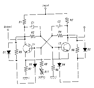
Fig: 1 is a circuit diagram of a bistable multivibrator circuit included
in a random number generator according to the present invention,
Fig. 2 is a circuit diagram of an electric power supply controlling
circuit for generating a driving voltage to be applied to the bistable
multivibrator
circuit,
Fig. 3 is a circuit diagram of a buffer circuit for measuring and out-
putting the collector voltage of one transistor in the bistable multivibrator
circuit,
Fig. 4 is a binary frequency distribution of a random number
generated by a random number generator and random number generating method
according to the present invention, and
Fig. 5 is a binary frequency distribution of another random number
generated by the random number generator and the random number generating
method of the present invention.
DESCRIPTION OF THE PREFERRED EMBODIMENTS
[0013] This invention will be described in detail with reference to the
accompanying drawings.
Fig. 1 is a circuit diagram of a bistable multivibrator circuit included
in a random number generator according to the present invention. The bistable
multivibrator circuit illustrated in Fig. 1 is constructed of, as fundamental
circuit
parts, transistors Tl; T1, collector resistances R1; R2, feedback resistances
R3;
R4, and biasing resistances R7, R8, R9; R11, and as supplemental circuit
parts,
02087 (2002-282,842)
CA 02441887 2003-09-22
-4-
condensers C1; C2, resistances R5; R6, and diodes D1-D4 for wave-shaping.
[0014] In order to realize the bistable multivibrator circuit, the transistors
T1
and T2 are made of the same transistor in characteristic value. The resistance
values of the collector resistances R1 and R2 are set equal to each other, and
the
resistance values of the feedback resistances R3 and R4 are set equal to each
other.
Also, the capacities of the condensers C1 and C2 are set equal to each other.
Herein, it is not always required to set the resistance values of the
resistances R5
and R6 and the characteristic values of the diodes D1-D4 equal to one another.
Generally, however, it is desired that the characteristic values of the
supplemental
circuit parts such as the resistances and the diodes are set equal to one
another.
[0015] When a given driving voltage is applied to the bistable multivibrator
circuit from the input, one of the transistors T1 and T2 is rendered
conduction in
electric current and the other is rendered shut in electric current. In this
case, if
the characteristic values of the transistors Tl; T2, the resistance values of
the
collector resistances R1; R2, the resistance values of the feedback
resistances R3;
R4, the capacities of the condensers C1; C2, and the resistance values of the
biasing resistance R8; R9+R11 are set equal to each other, the conduction
states
of the transistors Tl and T2 can not be predicted, and thus, depend on noise
in
the bistable multivibrator circuit.
[0016] For example, numeral "0" is allotted to the conduction state of the
transistor T1 through switching operation (switch on), and numeral "1" is
allotted
to the non-conduction state of the transistor Tl through switching operation
(switch off). Since the conduction state or the non-conduction state of the
transistor T1 depends on the noise in the bistable multivibrator circuit, the
numerals "0" and "1" can be generated randomly, so that a given binary random
number can be generated.
[0017] The conduction state and the non-conduction state of the transistor T1
can be easily detected by measuring the collector voltage of the transistor T1
at
the output.
[0018] Generally, however, it is difficult to realize the above-mentioned
ideal
bistable multivibrator circuit only if the characteristic values of the
transistors T1
and T2 are set equal to each other, so that the transistors Tl and T2 are
likely to
be conduction state or non-conduction state stochastically. Therefore, the
02087 (2002-282,842)
CA 02441887 2003-09-22
probability in conduction state or non-conduction state of the transistor T1
is
larger than the probability in non-conduction state or conduction state of the
transistor T1 stochastically, so that the occurrence probability of the
numeral "0"
or "1" is larger than the occurrence probability of the numeral "1" or "0". As
a
result, a binary random number can not be generated.
[0019] In this case, the characteristic values of the circuit parts in the
bistable
multivibrator circuit are adjusted within a predetermined period of time to
render
the occurrence probability of the numeral "0" or "1" equal to each other
(occurrence probability=0.5). Therefore, since the conduction state and the
non-conduction state of the transistor T1 can be set randomly on the noise in
the
bistable multivibrator circuit, the occurrence probabilities of the numerals
"0"
and "1" can be set to 0.5, so that a given binary random number can be
generated.
[0020] In this embodiment, the resistance value of the biasing resistance R11
as a variable resistance is adjusted to realize the equal occurrence
probability of
0.5 relating to the numerals "0" and "1". The biasing resistance R11 may be
coupled in series to the resistance R8 on balance condition.
[0021] Fig. 2 is a circuit diagram of an electric power supply controlling
circuit for generating a driving voltage to be applied to the bistable
multivibrator
circuit illustrated in Fig. 1. In the electric power supply controlling
circuit
illustrated in Fig. 2, the output is coupled to the input of the bistable
multivibrator
circuit illustrated in Fig. 1.
[0022] In the electric power supply controlling circuit in Fig. 2, a given
biasing current is introduced into the circuit, and a given rectangular wave
is also
introduced into the circuit via the condensers C3 and C4. Then, the transistor
T3 is switched to generate and output a driving voltage at the collector for
the
bistable multivibrator circuit. Instead of the condensers C3 and C4, a single
nonpolar condenser may be employed.
[0023] Fig. 3 is a circuit diagram of a buffer circuit for measuring and
outputting the collector voltage of the transistor T1 in the bistable
multivibrator
circuit illustrated in Fig. 1. In the buffer circuit illustrated in Fig. 3,
the input is
coupled to the output at the collector of the transistor Tl in the bistable
multi-
vibrator circuit illustrated in Fig. 1. A given collector voltage measured at
the
output of the buffer circuit is supplied for calculation.
02087 (2002-282,842)
CA 02441887 2003-09-22
-6-
[0024] In the use of the buffer circuit illustrated in Fig. 3, the collector
voltage of the transistor T1 can be easily measured without the influence on
the
bistable multivibrator circuit illustrated in Fig. 2. Therefore, the binary
random
number can be generated easily and stably.
[0025] Figs. 4 and 5 are binary frequency distributions of random numbers
generated by using the random number generator comprised of the circuit
components illustrated in Figs. 1-3. Fig. 4 shows 5000 random number pieces
and Fig. 5 shows 10000 random number pieces. In Figs. 4 and 5, no checkered
pattern appears, and only dot-like pieces appears, which shows the generation
of
a binary random number.
[0026] Although the present invention was described in detail with reference
to the above examples, this invention is not limited to the above disclosure
and
every kind of variation and modification may be made without departing from
the scope of the present invention.
[0027] In the circuit diagram illustrated in Fig. 1, for example, if
condensers
C11 (0.001 ~F), C12 (0.1 ~,F) and C13 (1 ~.F) are coupled in parallel to the
line
between the input and the earth, the operation of the bistable multivibrator
circuit
can be stabilized. In the above embodiment, although the transistor T1 is
employed and driven in on/off switch, the transistor T2 may be employed and
driven. Also, numeral "0" may be allotted to the non-conduction state of the
transistor T1 and numeral "1" may be allotted to the conduction state of the
transistor T1.
[0028] Moreover, in the above-mentioned embodiment, although the biasing
variable resistance R11 for balancing the transistors T1 and T2 is coupled in
series to the resistance R9, it may be coupled in parallel. In addition,
instead of
the resistance R11, another variable resistance may be coupled in series or in
parallel to a resistance of the bistable multivibrator circuit.
[0029] As mentioned above, according to the present invention, with simple
and not expensive devices, a new method for generating random number with
more perfectly disorder and a random number generator which is utilized in the
generating method of random number can be provided.
02087 (2002-282,842)