Note: Descriptions are shown in the official language in which they were submitted.
CA 02442308 2009-07-31
INDUCTIVE CURRENT SENSOR FOR AN ELECTRICITY METER
Field of the Invention
The present invention relates to current sensors for measuring current flowing
in
conductors. More particularly, but not exclusively, the invention relates to a
current sensor forming part of an alternating current (AC) fiscal electricity
meter
for measuring the energy supplied by a utility company.
Background to the Invention
In a published PCT patent application PCT/GBOO/02851 (WO 01/11376), there is
described a current sensor which responds to a magnetic field generated by a
current flowing in a load conductor.
In a published United States patent no. 4,894,610 there is described a current-
transformer arrangement for a static electricity meter.
In a published PCT patent application no. PCT/GBOO/02604 (WO01114894) there
is described an electronic circuit formed on a printed circuit board which is
configured as a current-to-voltage converter using a printed circuit track as
a
-1-
CA 02442308 2009-07-31
sensor, the sensor being placed in parallel with a primary current carrying
conductor, for example a bus bar.
Situations arise where a current sensor is required having the following
characteristics:
a) a load current bearing conductor having a simple linear shape;
b) a sensor scaling factor susceptible to modification merely by altering
dimensions of the sensor in one direction;
c) a circuit board real estate which is used efficiently and is substantially
rectangular in format with a minimum number of vias and/or cross-overs;
and
d) virtual immunity to remotely generated alternating magnetic fields.
Current sensors described in the aforesaid PCT applications and US patent are
not capable of providing simultaneously all the characteristics (a) to (d)
above.
Summary of the Invention
In a first aspect of the present invention, there is provided a current sensor
comprising:
a number of conductor paths for carrying a number of currents to be sensed,
and
sensing means for coupling to a magnetic field pattern generated by a flow of
current in said conductor paths;
wherein said sensing means comprise a substantially planar arrangement of
conductive elements, consisting of:
a first coil comprising a first inner coil portion having an effective
magnetic centre
at a first location (Cl), and a second outer coil portion having an effective
magnetic centre at the first location (Cl) wherein the first coil has a
central region
of positive response to time-increasing magnetic field perpendicular to the
plane
of the said coil, surrounded by a region of negative response to said magnetic
-2-
CA 02442308 2011-02-17
field and wherein the region of positive response is centred at the first
location
(C 1); and
a second coil, in a plane substantially parallel to said first coil,
comprising a third
inner coil portion having an effective magnetic centre at a second location
(C2),
and a fourth outer coil portion having an effective magnetic centre at the
second
location (C2), wherein the second coil has a central region of negative
response
to said magnetic field surrounded by a region of positive response to said
magnetic field and wherein the region of negative response is centred at the
second location (C2);
1o wherein the first coil and the second coil are located relative to each
other so that
along the line joining C1 and C2, the region of positive response of the first
coil to
said magnetic field substantially coincides with the region of positive
response of
the second coil to said magnetic field and so that the region of negative
response
of the second coil to said magnetic field coincides with the region of
negative
response of the first coil to said magnetic field.
According to one aspect of the invention, there is provided a current sensor
comprising:
a number of conductor paths for carrying a number of currents to be sensed,
and sensing means for coupling to a magnetic field pattern generated by the
flow of current in said conductor paths;
wherein said sensing means comprising a substantially planar arrangement of
conductive elements, consisting of-
a first coil comprising a first, inner, coil portion having an effective
magnetic
centre at a first location (Cl), and a second, outer, coil portion having an
effective
magnetic centre at the first location (Cl); wherein said first coil portion
and said
second coil portion are wound in opposite directions; said first coil portion
and said
second coil portion being connected by a conductor or by concatenation,
whereby
the first coil has a central region of positive response to time-increasing
magnetic
field perpendicular to the plane of the said coil, surrounded by a region of
negative response to said magnetic field and wherein the region of positive
response is centred at the first location (Cl); and
-3-
CA 02442308 2011-02-17
a second coil, in a plane substantially parallel to said first coil,
comprising a third,
inner, coil portion having an effective magnetic centre at a second location
(C2),
and a fourth, outer, coil portion having an effective magnetic centre at the
second
location (C2); wherein said third coil portion and said fourth coil portion
are wound
in opposite directions; said third coil portion and said fourth coil portion
being
connected by a conductor or by concatenation; whereby the second coil has a
central region of negative response to said magnetic field surrounded by a
region
of positive response to said magnetic field and wherein the region of negative
response is centred at the second location (C2);
io wherein the first coil and the second coil are located relative to each
other so that,
along the line joining C1 and C2, the region of positive response of the first
coil to
said magnetic field substantially coincides with the region of positive
response of
the second coil to said magnetic field and so that the region of negative
response
of the second coil to said magnetic field coincides with the region of
negative
response of the first coil to said magnetic field.
Such a sensor is capable of one or more of the following:
a) operating in conjunction with a load current bearing conductor having a
simple linear shape;
b) providing a sensor scaling factor susceptible to modification merely by
altering dimensions of the sensor in one direction;
c) occupying a circuit board real estate which is used efficiently and is
substantially rectangular in format with a minimum number of vias and/or
cross-overs; and
d) being substantially immune to remotely generated alternating magnetic
fields.
Preferably, to improve manufacturability and reduce cost, the elongate
elements
3o are implemented in the form of conductive tracks on a printed circuit
board.
-3a-
CA 02442308 2009-07-31
On account of the use of a transformation described later, it is feasible to
reduce
the need for track cross-overs and thereby largely circumvent the need to use
circuit board vias. Thus, the elongate elements of the sensor are preferably
interconnected on the circuit board substantially without the need to use
vias.
More preferably, the printed circuit board is a multi-layer board and the
elongate
coil elements are duplicated at a plurality of levels in the board and
corresponding
overlaid zones coupled together in order to enhance current measuring
sensitivity
of the sensor.
For example, the elongate coil elements are preferably duplicated at several
of
the layers in the form of a stack and connected in series to provide an
increase in
output signal magnitude resulting from magnetic fields generated by current
flow
in the one or more conductive paths coupling into the stack.
Preferably elongate coil elements of the overlaid zones are interconnected at
regions remote from where the one or more load conductors couple magnetically
to one or more of the elements. Implementing interconnection at regions remote
for active coupling zones of the sensor enables a greater sensor measurement
sensitivity to be achieved.
Insensitivity of the sensor to uniform remotely-generated magnetic fields is
an
important performance characteristic of the sensor. Especially when the sensor
is implemented comprising a stack of elongate coil elements, there is tendency
for the sensor to become sensitive to uniform magnetic fields incident
parallel to
the plane of the sensor. By alternately swapping connection of elongate
elements in the several layers, it is possible to arrange for EMFs generated
by. in-
plane uniform fields to mutually oppose rendering the sensor substantially
immune to such uniform fields. Thus, preferably, the elongate coil elements
are
connected alternately between layers so as to render the sensor less sensitive
to
uniform magnetic fields incident on the sensor having field components
parallel to
the plane of the sensor.
-4-
CA 02442308 2009-07-31
Conveniently, in order to render the sensor more efficient in its use of
circuit
board real estate, the elongate coil elements are preferably arranged so that
their
elongate axes are substantially mutually parallel.
In order for the sensor to provide a substantially linear measurement response
for
a wide range of currents conveyed through the sensor to the load, the elongate
coil elements are preferably non-ferromagnetically coupled to the one or more
conductive paths. The use of ferromagnetic components in the sensor would
1o impart thereto an upper limit of linear measurement due to ferromagnetic
component magnetic saturation.
In cost sensitive applications, it is desirable that the sensor is capable of
providing
a measure of average current plurality of conductive paths. Therefore, the
sensor
is preferably arranged such that a plurality of the conductive paths are
disposed
on opposing major faces of the plane encompassing the elongate coil elements,
the sensor thereby providing in use an output signal indicative of the
summation
of the one or more currents flowing in the plurality of conductive paths. By
scaling
the summation by the number of current paths present, a measure of average
current flow in the current paths can be achieved.
The sensor can be supplemented by one of more voltage sensors for power
measurement purposes. Therefore, the sensor preferably further comprising
voltage sensing means for sensing substantially the voltage of the power
source
and generating a corresponding voltage measure. A product of the current
measure and voltage measure enables a measure of power to be calculated.
When the sensor is used to measure power, the sensor preferably further
comprises signal processing means for integrating the current measure with
3o respect to time to provide an integral current measure and computing means
to
compute a product of the integral current measure and the voltage measure to
derive a measure of energy consumed by the load.
-5-
CA 02442308 2009-07-31
In order to render the sensor relatively inexpensive to manufacture when
adapted
for power sensing applications, the signal processing means and the computing
means are preferably integrated onto a single silicon integrated circuit.
Advantageously, the sensor preferably further comprises a memory for storing
calibration data for one or more of correcting scale factor, offset and phase
errors
within the sensor. Such calibration is important for many potential
applications for
the meter, for example especially when customer billing occurs on the basis of
1o measurements provided by the sensor. Moreover, calibration can often be a
time
consuming and therefore expensive procedure during sensor manufacture hence
recording calibration data in the memory is capable of facilitating more rapid
calibration during manufacture. The calibration data can, for example, be
subsequently used to scale output from the sensor when the sensor is in
operation. More preferably, the memory is also operable to store serial number
information and the measurement of power consumed by the load. In order that
data stored in the memory is not lost when power is removed from the sensor,
the
memory preferably includes non-volatile memory, for example EEPROM.
Remote interrogation of sensors is an increasingly important contemporary
operating requirement. Thus, preferably, the sensor comprises interfacing
means
for enabling the sensor to be remotely interrogated. More preferably, the
interfacing means comprises an Internet connection for enabling the sensor to
be
interrogated and/or to output measurement data via the Internet.
In a second aspect of the present invention, there is provided an electrical
energy
meter comprising one or more sensors according to the first aspect of the
invention for use in measuring and recording electrical energy consumed.
Preferably, the meter is configured in a 2S-type configuration; the 2S-type
configuration is defined later. More preferably, in order to reduce the number
of
current sensors required, the meter comprises a single sensor according to the
-6-
CA 02442308 2009-07-31
first aspect of the invention arranged to provide in use an average current
measure of currents flowing through a plurality of load conductors mounted in
close proximity to, or in contact with, the sensor. More preferably, the
plurality of
load conductors are mounted on opposing major faces of the single sensor.
Alternatively, the meter can be in a 12S-type configuration; the 12S-type
configuration is defined later.
Alternatively, the meter is preferably implemented as a three-phase meter and
is
1o provided with two current sensors and means for deriving a third phase
current by
way of performing a simultaneous equation solution to signals derived from
said
two current sensors. By using the solution, for example based on Blondel's
theorem, it is possible to reduce the number of current sensors required and
thereby render the meter less expensive to manufacture, simpler in
construction
and more compact.
Description of the Diagrams
Embodiments of the present invention will now be described, by way of example
only, with reference to the following diagrams in which:
Figure 1 is a cross-sectional view of a load conductor and a circuit board
with a
magnetic field around the load conductor;
Figure 2 is a plan view of a transducer;
Figure 3 is a view of a response characteristic of the transducer in Figure 2
to a
local magnetic field generated along a line XX' in Figure 2;
3o Figure 4 is an illustration of a current sensor comprising two transducers
of the
type shown in Figure 2 mutually superimposed;
-7-
CA 02442308 2009-07-31
Figure 5a is an illustration of an alternative connection arrangement for a
first
region of the current sensor of Figure 4;
Figure 5b is an illustration of an alternative connection arrangement for a
second
region of the current sensor of Figure 4;
Figure 5c is an illustration of an alternative connection arrangement for a
third
region of the current sensor of Figure 4;
1o Figure 6 is an illustration of a current sensor incorporating the
alternative
interconnection arrangements of Figures 5a, 5b, 5c;
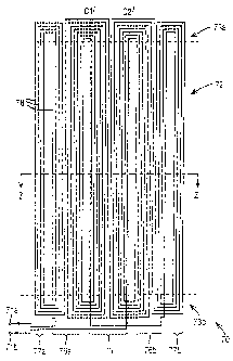
Figure 7 is an illustration of a current sensor comprising elongate
substantially-
linear coil elements;
Figure 8 is a diagram of a relationship between conductor elements of Figure 7
and the transducers of Figure 4;
Figure 9 is a schematic diagram of 2S-type and 12S-type fiscal electricity
meter
configurations;
Figure 10a is an isometric view of a three-phase fiscal electricity meter;
Figure 10b is a plan view of a circuit board forming part of the fiscal
electricity
meter of Figure 10a;
Figure 11 is a diagram of an electricity meter illustrating its principal
elements;
Figure 12a is a diagram of a first alternative configuration for elements of
the
meter of Figure 11;
-8-
CA 02442308 2009-07-31
Figure 12b is a diagram of a second alternative configuration for elements of
the
meter of Figure 11;
Figure 13 is a schematic block diagram of a sensor PCB sub-assembly for the
meter of Figure 11;
Figure 14 is a circuit diagram of the sensor sub-assembly of Figure 13; and
Figure 15 is a circuit diagram of a display PCB sub-assembly for the meter of
1o Figure 11.
-9-
CA 02442308 2009-07-31
Description of Embodiments of the Invention
Referring to Figure 1, there is shown a cross-sectional view of a printed
circuit
board (PCB) 10 and a load conductor 11. The load conductor 11 is mounted
above the PCB with a small separation, for example in a range of 0.5 mm to 4
mm, between it and the PCB 10. If required, the load conductor 11 can
alternatively be made integral with the PCB 10.
The load conductor 11 is shown with a current flowing through it into the
plane of
1o the drawing. This current produces magnetic field lines 12 which encircle,
in a
clockwise direction as illustrated by arrows on the magnetic field lines 12 in
the
drawing, the load conductor 11. To a left-hand-side of the load conductor 11,
the
magnetic field lines 12 rise out of the plane of the PCB 10 and are
concentrated
in a region whose effective magnetic centre is designated by M1. On a right-
hand-side of the load conductor 11, the magnetic field lines 12 descend into
the
plane of the PCB 10 and are concentrated in a region whose effective magnetic
centre is designated by M2.
An alternating current (AC) flowing through the conductor 11 results in a
sinusoidal variation in the strength of the magnetic field lines 12 with time.
In the
case of a 50 Hz mains supply, 100 reversals of the direction of the magnetic
field
lines 12 occur each second.
Figure 2 is a plan view of a substantially circular planar transducer 20. The
planar transducer 20 is described in an earlier published International PCT
application no PCT/GBOO/02851 (WO01/11376). The transducer 20 is formed as
conductive tracks on a printed circuit board and comprises a sense portion 21
and a cancellation portion 22. As illustrated, the sense portion 21 is a
spiral coil
comprising four turns, each turn having a radius of substantially r1. The
cancellation portion 22 is a single turn of radius r2. The effective magnetic
centres of the sense portion 21 and of the cancellation portion 22 are
substantially co-located and are shown at Cl; C1 corresponds also to a spatial
-10-
CA 02442308 2009-07-31
centre of rotational symmetry of the portions 21, 22. The radius r2 of the
cancellation portion 22 is substantially double that of the sense portion 21.
Thus,
even though
-11-