Note: Descriptions are shown in the official language in which they were submitted.
CA 02442332 2003-09-26
WO 02/080357 PCT/US02/09478
VARIABLE GAIN LOW-NOISE AMPLIFIER FOR A WIRELESS
TERMINAL
BACKGROUND OF THE INVENTION
This application claims priority to U.S. Provisional Application Serial No.
60/279,451, filed March 29, 2001, whose entire disclosure is incorporated
herein by
reference.
1. Field of the Invention
This invention relates generally to a circuit for controlling gain in low
noise
amplifiers (LNA's) or in preamplifiers, and more specifically to gain control
circuitry for
use in LNAs or preamplifiers used in wireless communication systems.
2. Background of the Related Art
In wireless communication, the incident signal at a terminal unit (e.g. an
handset)
has various magnitudes, depending on the environment of the radio-wave
propagation
(including the distance between the terminal and the base station). A strongly
radiated
signal from a transmitting terminal is helpful to a remote station, but is of
less use if the
station is nearby. Such a strong signal may impose unwanted spurious signals
on foreign
terminals near the transmitter, and waste the transmitter's battery.
Additionally, the
circuit for amplification in a receiving terminal may clip and distort its
output signal for
a large magnitude input.
In general, the inward and the outward signal in a terminal are amplified by a
low-
noise amplifier (LNA) in the receiver block and a preamplifier in the
transmitter block,
respectively. Good linearity must be achieved in order to suppress the
distortion in the
next stages. To prevent the LNA from clipping its output signal for a large
input, the
LNA's gain has to be made controllable (the gain being lowered fox large input
signal).
Similarly, the gain of a transmitter's preamplifier must be controlled so as
not to waste
the battery and also not to overdrive its next stage, the power amplifier.
Figure 1 shows a related art low noise amplifier that employs current-
splitting
gain-control techniques. In related art gain-control schemes, the LNA's gain
is decreased
-1-
CA 02442332 2003-09-26
WO 02/080357 PCT/US02/09478
by reducing the drain bias current (i.e., by decreasing the gate bias voltage)
of its subcircuit
responsible for the gain, i.e., a differential-amplifier stage. If the
magnitude of an input
signal exceeds some prescribed level, then the LNA is entirely bypassed so
that no
amplification occurs. Unfortunately, the reduction of the bias curxent is
accompanied by
degradation of linearity caused by an unwanted cutoff of the driving
transistor. An abrupt
change of LNA's gain inherent in the bypass operation makes it hard to
simultaneously
achieve good linearity and the desired noise performance. Accordingly, a new
approach is
desirable to control the gain.
SUMMARY OF THE INVENTION
An object of the invention is to solve at least the above problems and/or
disadvantages and to provide at least the advantages described hereinafter.
Another object of the invention is to provide a method and apparatus for
controlling
gain in a low-noise amplifier or in a transmitter's preamplifier.
Another object of the invention is to provide a low-noise amplifier and method
of
operating same that reduces or avoids clipping its output signal when
receiving a large input
signal.
Another object of the invention is to provide a method and apparatus capable
of
controlling the gain of a teansmitter's preamplifier so as not to waste the
battery and not to
overdrive the next stage (the power amplifier).
In a preferred embodiment of the invention, a variable gain amplifier
includes, at least
in part, a first transistor having a control electrode, a first electrode, a
second electrode and
a drain, wherein an input sigYial is coupled to the control electrode, a first
reference voltage
is coupled to the first electrode and an output signal is coupled to the
second electrode; a
load inductor coupled between a second reference voltage and the second
electrode of the
first transistor; a load capacitor coupled to the second electrode of the
first transistor; and
a variable resistor coupled in parallel to the load inductor.
_2_
CA 02442332 2003-09-26
WO 02/080357 PCT/US02/09478
In another preferred embodiment of the invention, a multi-frequency amplifier
includes, at least in part, a driving transistor having a source, a gate and a
drain, wherein an
input signal is input by an input terminal coupled to the gate, the source is
coupled to a
reference voltage source, and an output signal is output by an output terminal
coupled to the
drain; a load inductor coupled between a power voltage source and the output
terminal; a
load capacitor coupled between the output terminal and the reference voltage
source; a
variable resistor coupled between the power voltage source and the output
terminal in
parallel to the load inductor; and at least one pull-up capacitor deployed in
paxallel with
the load inductor wherein each of the at least one pull-up capacitors are
independently
selectable by a plurality of switches coupling each of the at least one
capacitors with the load
inductor.
Additional advantages, objects, and features of the invention will be set
forth in part
in the description which follows and in part will become apparent to those
having ordinary
skill in the art upon examination of the following or may be leaxned from
practice of the
invention. The objects and advantages of the invention may be realized and
attained as
particularly pointed out in the appended claims.
BRIEF DESCRIPTION OF THE DRAWINGS
The invention will be described in detail with reference to the following
drawings in
which like reference numerals refer to like elements wherein:
Figure 1 is a circuit diagram of an LNA with current-splitting gain-control
technique
according to the related art;
Figure 2(a) is a circuit diagram of a low-noise amplifier with a desired gain
in a narrow
band of frequencies according to an embodiment of the invention;
Figure 2(b) is a circuit diagram of an embodiment for the amplifier in Figure
2(a)
~5 according to an embodiment of the invention;
Figure 2(c) is a circuit diagram of a PMOS transistor operating as a switch
with a turn-
on resistance according to an embodiment of the invention;
-3-
CA 02442332 2003-09-26
WO 02/080357 PCT/US02/09478
Figure 3(a) is a circuit diagram illustrating a circuit designed to reduce
power
consmnption by providing a variable conductance parameter k which is achieved
by dividing
the driving transistor MN1 into distributed NMOS transistors MN[1]~MN[n]
according to
an embodiment of the invention;
Figure 3(b) is a circuit diagram of the PMOS switches which turn the NMOS
transistors MC[1]~MC[n] on and off according to an embodiment of the
invention;
Figure 4(a) is a circuit diagram illustrating a circuit which is capable of
switching
between two resonant frequencies according to an embodiment of the invention;
and
Figure 4(b) is a circuit diagram illustrating a generalized version of Figure
3(a) which
LO enables multi-band operation using a single driving transistor MN1,
according to an
embodiment of the invention.
DETAILED DESCRIPTION OF PREFERRED EMBODIMENTS
A gain-control method and apparatus for a low-noise amplifier (e.g., tuned)
and a
preamplifier used in wireless communication systems will be described
according to
preferred embodiments of the present invention. For example, one preferred
emboclitnent
of the gain control method and apparatus can be adopted for the circuitry in a
wireless
terminal and implemented in an LNA or a preamplifier. However, the present
invention is
not interpreted to be so limited. Further, the invention is applicable to any
type of device
technologies, such as the bipolar-junction transistor (BJ'I~ or junction field-
effect transistor
QFE'I~. For purposes of illustration, preferred embodiments according to the
invention will
be described below using metal-oxide-semiconductor field-effect transistor
(MOSFE'1~
technology.
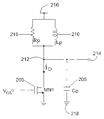
Figure 2(a) is a diagram that shows a preferred embodiment of an amplifier
according
to the present invention. Figure 2(a) shows a tuned LNA which has a desired
gain in a
narrow band of frequencies. The LNA may be constructed with an n-channel MOS
(NMOS) transistor MN1 200 and a load composed of a capacitor Cp 205, an
inductor Lp
210, and a resistor Rp 215. An input signal may be applied at the gate node of
the common-
-4-
CA 02442332 2003-09-26
WO 02/080357 PCT/US02/09478
source NMOS transistor (MN1) 200, and its amplified signal may appear at the
drain node
212 or an output terminal 214 may be coupled thereto. Preferably, the resistor
Rp 215 and
the inductor Lp 210 are coupled between a power supply voltage 216 (e.g., Vdd)
and the
drain node 212, and the capacitor Cp 205 is coupled between a ground terminal
218 and the
drain node 212. The capacitance Cp 205 may be attributed to the input
capacitance of the
next stage (e.g. a mixer) and/or parasitic capacitance at the output node. The
inductor Lp
210 preferably forms a parallel-resonant circuit with the capacitor Cp 205,
and tunes the
LNA's gain at a desired frequency, locating the peak of gain at the resonant
frequency. The
inductor 210 may be implemented using a spiral or a bond-wire inductor (or by
using an
external inductor).
To adaptively control the gain of the LNA and avoid the input signal
distorting the
output (by saturating or cutting offj, resistor Rp 215 may be variable
according to one
preferred embodiment of the invention. Reducing the drain bias current (i.e.,
the DC
component of iD in Fig. 2(a)) in order to lower the gain for increased
magnitude of input
signal saves power, but involves a possible degradation of linearity caused by
the unwanted
cutoff operation of MN1 200. Decreasing the value of Rp 215 in Figure 2(a) to
lower the
gain, however, does not affect linearity of the LNA. Hence, to change gain, Rp
215 may be
controlled rather than the drain bias current, provided the linearity is more
important than
reduction of power consumption.
The gain is proportional to Rpz at the resonant frequency. Accordingly, the
gain is
proportional to the quality factor QZ of the resonant circuit (i.e.,
proportional to the
sharpness of the gain peak) for fixed values of Cp 205 and Lp 210, since the
quality factor
Q of the resonating load is directly proportional to Rp 215:
Cp
Q = Rp L (Eq. 1) Hence,
p
controlling Rp 215 is equivalent to controlling Q for fixed values of Cp 205
and Lp 210.
-5-
CA 02442332 2003-09-26
WO 02/080357 PCT/US02/09478
Figure 2(b) shows a preferred embodiment of a circuit implementation for the
amplifier in Figure 2(a). The variable resistor or a variable resistance as
shown in Figure 2(b)
is implemented with the p-channel MOS (PMOS) transistors MP (1]~MP[n] (220,
225, 230)
aligned in parallel. Each PMOS transistor is made to operate in its linear
region when turned
on (i.e., when its gate voltage is lowered), so it can be regarded as a switch
with a turn-on
resistance as shown in Figure 2(c). The net resistance is controlled by the
logic of the gate
signals ctrl[1]ctrl[n] (235, 240, ... 245). Controlling these PMOS switches
one by one, the
amplifier's gain is adjusted stepwise. The amplifier has minimum gain when all
these PMOS
switches are turned on (by lowering all their gate voltages).
A common-gate NMOS transistor MC1250 is added to further isolate the input
from
the output, reducing the Miller effect. The bias-generating block BIAS_GEN1
255 keeps
the operation of MC1 250 unaffected or less affected by the swing of the
output signal by
maintaining MC1 250 in the saturation region.
It is true that decreasing the load's Q degrades the linearity less than
reducing the DC
bias current, but at the expense of higher power consumption relative to other
approaches.
To maintain the linearity with the circuit in Figure 2(b), the drain bias
current must be
maintained, being accompanied by a constant DC power consumption. Because the
conductance parameter k (proportional to the gate width) of MN1200 is fixed
for the circuit
in Figure 2(b), it is impossible to reduce the amplifier's DC power
consumption. If the DC
power consumption must be reduced, a new approach of gain control may be
necessary.
To reduce the power consumption by making k variable, a circuit in Figure 3
(a) may
be used in a preferred embodiment according to the present invention. As shown
in Figure
3(a), the driving teansistor MN1 200 is divided into the distributed NMOS
transistors
MN[1] ~MN[n] (e.g., 300, 305, ... 310). These transistors are controlled by
the corresponding
NMOS transistors MC[1]~MC[n] (e.g., 315, 320, ... 325), which are respectively
turned on
and off by the corresponding PMOS switches 330, 335, ... 340 also illustrated
by example
in Figure 3 (b). As the magnitude of the input grows, it may be preferable to
inexease the gate
bias voltage with BIAS GEN2 345 signal in Figure 3 (a) to maintain the
linearity. To
-G-
CA 02442332 2003-09-26
WO 02/080357 PCT/US02/09478
decrease the gain and reduce the DC power consumption at the same time, it may
be
preferable to decrease the value of k at a much faster rate than the rate of
increase of the gate
bias. Here, a trade off is needed between the reduction of power consumption
and the
smoothness of gain control, since the fast variation of k entails widened gaps
of gain steps.
Advantageously, smoother gain control results if the pull-up resistor (Rp) 350
is made
variable as described for Rp 215. In one preferred embodiment, the variable
resistance may
be implemented with p-channel MOS (PMOS) transistors as in Figure 2(b).
The circuit in Figure 3(a) may also be used for a transmitter's preamplifier
in a
wireless terminal unit, but in this case it may necessary to place a low
capacitive load at its
output. This is because a typical preamplifier drives the power amplifier
whose input
impedance may be set to 50~ (a standard impedance in microwave engineering).
A pull-up capacitor Cp' 400 may be connected in parallel with the pull-up
inductor
Lp 410 and turned on and off with its series-connected switch 405 as shown in
Figure 4(a).
For this preferred embodiment according to the invention, switch 405 may be
implemented
with a complementary-MOSFET (CMOS) "transmission gate," in which case the
resonant
frequency may be shifted down and up correspondingly. The resonant frequency
may be
made to fall on another desired frequency band, provided that the amplifier
functions stably
at the shifted band. One example of dual-band operation may be an amplifier
for wireless
communication, usable for a cellular band around 800 MHZ and a PCS band around
1800
MHZ (time-multiplexingly). The desired frequency band may be selected by an
external
signal that controls the CMOS switch. Additional band selectivity may be
achieved by
employing the circuit shown in Figure 4(b), which is an alternative preferred
embodiment
to the circuit in Figure 4(a). The preferred embodiment shown in Figure 4(b)
can achieve
mufti-band operation with a single driving transistor MN1 415. In operation,
capacitors
Cp' [1] - Cp' [n] (e.g., 420, 425, ... 430) may be turned on and off
discretely or
combinationally by corresponding series-connected switches (e.g., 435, 440,
... 445) (such as
the CMOS transmission-gate switches).
-7-
CA 02442332 2003-09-26
WO 02/080357 PCT/US02/09478
As described above, preferred embodiments of methods and apparatus for gain
control in a wireless communication system have various advantages. To avoid
the clipping
distortion of the output signal of an integrated preamplifier or low-noise
amplifier employing
MOSFET technology (e.g., in a terminal unit for wireless communication), the
gain may be
made adjustable by incorporating a variable resistor in the pull-up load
according to the
preferred embodiments. The variable resistor may be implemented using
distributed PMOS
transistors operating in the linear region as shown in Figure ~(b). Also, to
attain the
controllability of the DC power consumption as well as the gain
controllability, a driving
transistor may be divided into the distributed transistors in a preferred
embodiment, which
can be turned on and off individually. In addition, a resonant frequency can
be adjusted
and/or a mufti-band operation may be implemented in a preferred embodiment by
selectively coupling an additional capacitor or the like in parallel with a
load inductor.
The foregoing embodiments and advantages are merely exemplary and are not to
be
construed as limiting the present invention. The present teaching can be
readily applied to
other types of apparatuses. The description of the present invention is
intended to be
illustrative, and not to limit the scope of the claims. Many alternatives,
modifications, and
variations will be apparent to those skilled in the art. In the claims, means-
plus-function
clauses are intended to cover the structures described herein as performing
the recited
function and not only structural equivalents but also equivalent structures.
_g_