Note: Descriptions are shown in the official language in which they were submitted.
CA 02442375 2003-09-24
1.
IMp80V~EN'1'S IN .A.1~TD RELATING TO ?~N.~LOG~ MAINTENANCE
DETFCTT01~1
Fi.Ald of the .Islvcatiaus
The present inzrPnl-ion relates to methods and appa.catus
sui table for the proces~i nc~ of optical signal., modulated
by lover frequmc:y siqnalS Such as anal o~stA maintanamce
signale. Sucli methods and a~~dratus are suitet~tP tor: but
oot liznitod t:o, improving the detectability of analoc_~ue
maintenance ~i ~.alc .
8ackgrouad of the taventioa
Modern optical commun.icatiorl systcnis, 5uc:h as those uSAd.
in the telecommunicationo fic~.d, typica7.ly use ~nravel~~yLxx
division mult:ylexinc~. GJa.vr~length division xnultiplc~sing
(~nTDMj .is tree serzdiYiq of signals of diftc~rpni-. wavelen?ths
2o simulta.x~eously along the same Lrarismission mc~c3imm
(xxormally an opts. cal fibre) . Lac:H of the separate
wavelengths ca.n carry a ecparate inforztsation siu,~~,a1 J l.luu5
allowing the simw:l,tanarny~ transmission of a r~umber of
vliffe.~ellt Sic.Tr~a,ls . Ty~iCally, each wave I Pnc~th utilised to
2,5 carry an 111fUZL1lc't1.1U11 ,.~'l~JIli'll is referreQ to as a Channel.
Informatior~ is: earriod within each cha~~arseZ by moc~ulal.i~y
the Optical signal a1-. a rr~latively high speed e.g. bit
rates of 2.5Gbls to ~UGb/s are commnn_
Analogue ma.int:enamce i5 the application of a relatively
1 nw fr_ pc~lAney tone ( less than the ix~for~nation bit rate) ,
at a relatively small ~m~lifio.We to the optical signal.
CA 02442375 2003-09-24
Z
FOr instanCC, t011es WiLxl3.n Lhe frequency range ~nokT~2 to
4001r~-I~ may 1=c u3ed. Such a fr~c~uenoy is utilised to
amrlitude modulate the optical inforniaLiuli signal at a
relatively ~m~'il modulation depth c.g. 1Rs of the peak
power of the ~~pLical signal.
Analogue mair;tenance signals c:drl be utilised to Carry
signalling data, for instance inaiCaLive uL' the source of
the r. p1 Rv,~.x~.t channel, or for control of the optical
z0 rletwork , )r'om examp I P,. ~ each channel within, a WDM vigr~.al
may Le ~.lloc;dted a frecxueney ba~Cid within the r~nr~e 3flOkH2
400kH~, each band covering ~ic~~.~t separate frequenri_P~
separated by 32Hz . Nigxlalling imformaLioil can Lhus be
tran~mi tted bar applying izr turn different sequences of the
eight frequenc:.i p~ fin mr~dulate the relevaxxt optical signal .
As the r~malc>guc maintenance siGnal is applied at a
predEtcrmincd propoa:tion of the up~ic;d1 signal power.
d.Ptertion an<~, datex'mi.nation of the amplitude of d.i1
zU analoq»P m,~ini.-enance signal can be uoed tv calculate the
power 1n the relevant channel, r~t~»~ pas.i_1y allowing the
mona.toring of l.lle pezvoxittance Of an optical link.
Fi~,are 1 shows an optical network 100, incluaiy a muae
200. The nor3F~ x(.10 inr_ludes apparatus for tho detection of
2us dzlalocTUe maintenance ~i gna I . In this instance, the
node 200 also illc:ludes a receiver 300 for detecting at
least ono of the information signals rra~~,i~a by a relevant
channel. The recciv~r 300 will typically include d WDM
jU demultipl PXRr, arranged to demultip~.ex the optical sig~n.er,7.
into individual charmPl~. Each individual channel can
therx be dstected Ly a. prloto de>=eC'tor .
CA 02442375 2003-09-24
3
,Asz opl.ical 5i~mcll, C:U1ILY1'151I1C3 a x~.uzt~aer of channels, is
rcccivcd Eton', the rest of the network 100 by the node 200.
The rnajoxzty of this signal is passed to the receiver 300.
rx'edPtermir~ed rroportion of the signal (tyrically 1~
5~) is remo~cr'e~d bx optical tap zlU, and passed to a photo
detector 22 0 , suCx1 as a pho'COC~iod~ . The photo detector
converts the optical signal to an electrical sig~.~al _ For
convenicnac an. amplifier 230 amplifies the electxvcal
signal, the «utput voltage of the ampl.a.fier being passed
:1U to both a hanr3 pass fi I tPr »c.) and. a. .Low sass filter 240 _
The low pass filter 240 is arranged to pass only vary low
frequency cc~mponcnts of the electrical signal (e. g.
signals less than lkHz), with 'the resulting DC output
1 S vnl tac~p 'hPi n~ i nr7i c~~fi.a..vP of 'the total power of the ortical
slcf~,a1 i.e. the sum of the powers within each channel.
The band pa3~3 filter 250 is arranged to filter out both
the DC component of thA input signal, and th~ high
20 frer_~_tenr_y r~o~rponpnts (a_g_ thc~sr~ frAC,~uonr_iAS r_orr~spnnr_Zing
to the b~.t-rate of the information signal) , and hence to
ya.ss trxose frequencies corresponding to the analogue
znaintcnamce signals. Typically-, the band pas3 filter may
be arraz~,ged 1;o pass frequencies within the range lkHz to
IMH~.
The signal passed by the band pass filter will thus
contain frequency signals corresponding to each of the
analogue maintenance eignalE for each channel. By
30 mr~asurinrJ tr.e relative amplitudes of mach frer_h_tenr_.y
cnmpnnPnt , t~ha rPlar i.vc~ pn~snrPrs of each channel within the
upLic.~l 5ic>.mxl c:ati k~~ ci~'L~:cmimc~ (a5 Lrie ,~UWCt U.C a
maintenance :signal is a predetermined proportion of the
CA 02442375 2003-09-24
total signal powAr~ . l~,s the total ,~uwar of the oprin~l_
signal can be: dc~t.Prm.ined from the output of Lhe low pass
tiltez 240. eonSequPni-.ly the optical power per charnel can
be dete~-mi~,mc7.. Further. by analysing the e::act fxequez~cy
present at ~,ny given, instance, Lhe signal i xifarmation
r_arripd by the analogue main l.erlance signal Can he
determined_
Typically , to determine the .rpl Pe~ant frec~u.ency eouriponeats
and amplitudes of the aixalocN.e ma.intc~nanne sisals, the
omtput of the band pass filter 250 is passed to an
analogue t-.n digital convertcx 260, which cliyitiaes the
~siCinal. The rp~~_vl'ting digital oignal is passed ~u d
d~,giLal signals proceSSOr ~7ft, which can d~termine both the
25 frequency cumpuu~nLS and atfC~litudc~s c, f. the frequex~cy
comporxentc px~caent.
Stimulatpc~ R.anuan Scatt~aring (SR.6y results in the ~:LdIlSfer
~.C opLiCal povlex' between ~7i f.ferr~nt wav~langths of optical
zo signal bei=y transmitted simult-.anenusly along a
tranomicsion znedium such ei5 vpcica~, fibre. The pnwc?r
t-.r~nsferxed hettveon the different wav~7.~ngths is a
function of i-:hP instar~tanaous channel powers.
25 rigure 2 illustrates the Haman gain. c-:c~affiCi~nts for a
typical opticml fibre W 1 t'cla.tiUn Lo a pulp si ~3n~ I a'~
153 onm. Wit,h~.r. the graph., the soJ.ia lime izidieates the
actual Raman gaa.n aoaffieient, with the dotted line
~indiCating an ~pprn.ximation, o~ the Raman gain coefficient
JO g Lha(: can be used. Lo Simplit~r the R.ama.n power transfer
calcult~tion. X15 c:cizt be seen, Lhe AZaman gain nnr~ffi.ri2nt
within this raz~ge inerca3es with iacreasiilc~ wavelenqLh.
CA 02442375 2003-09-24
J
C:011S1PC~(7PT~~ly-, aTl opt1C31 ~1g11a1 lnGOt'jJUL'dtinCf two or more
c:hanx~,els at separate wav~length will see pOWe~, k~einy
transfetxed from zhP lower wavelength channel to the
higher wav'elE:lscJ, th channel as thQ si~'nal is tran.cznitted
along the optical fibz;e.
It is an ai m of embodiments of the pr esent itlY~IYtlOIl t0
provide apparat,~s anr~ methods for improved optical
processiy of art optical signal, so as to impxove the
detection of s:he amalo~ue maintenance sianal_
summarir of t~~a z~c~ntion
In a Li:G'st ~~SpGCL, 'the prPfipnfi invention providc3 an
apparatus fut Y~'OCessinG' arx optical ~i yn.al, the optical
signal Comprising at least. a .Cirsz Charinel, signal at-. a,
first ~nravelenc~th modulated by a first itec3uenc3T, a second
chazlnel signal at a s~cond wavolcngth module.ted Ly .d
seuciid frequency, and a thi rd channel sigzial at a thi,xd
wavelen~L~~ ~uvdulated by a third trpr~.iency, the apparatno
comprising: an input fv,~ Lec;eiving the optical signal ~ a
spl i~t~tQr arranged to split 'txl4~ l~CCiVCL3. c~pzica~. Signal
into at least two ortical bands, a fir3t optical. Lz~mcl
conlfrtising at least ~:hr~ tirst axed second channel signals,
~5 and a secmla optical band corilprising afi. lpa.st th~ th~.rd
channel Elgna,/,; ax~,d a fi~:sL ~xmto detector arranged to
rpceivo the first optical band, amcl Lc output a firS~G
eleeLx'iCal signal rroportional to the total optical pwsnre~
of the first o;~tica l hand .
J U
sy processing the optical sid'rlal in this ca~a~r, fi,he largest
va i us compoaer.~ts of ghost a.rnalo~-ue mai~Weziance s~.cmals
( f ormed b~,r SR:~ t runs f orrirg power bEtwcen the di f f erGiz L
CA 02442375 2003-09-24
6
chaxulals ) c,axi be relnV V ec3, axed Lllus the analogu~
mairitengnc-.P detection error due to SRS IeduLed.
Pr~fesd?~ly, tile apparatms forth~r comprises a first
clectricnl fil~ex~ arranged to filter the first elec trical
signal so as tv pas5 Said tirsL freque~ry and to block
s~i~7, third frequency; a second photo detector arranged
t~
receive t~'hP second
~~econd optical
band, and to
ou~,~ut a
electrical Si~~r131 pro~sc~rr.~.onal to the total powa~
optical
of the secorirl filter
optical band;
anal a second
electrical
arranged to as
filter LHe to
secozld electrical
~i c~n.al so
pasa said, t:zird frequezzcy' amr.'L l.~ block said fi
rst
trequenr_y .
1~ Pr~L~~,wT~ly the aDnaratus f,.~.rthpr eompriseo an. adder
arranged to sLUn the ;~iltexed elecCrical si g-na'1 s
Prpfprably, the apparatus further coillpri5es a si.,qllal
processinS~ unit arra.n~ed to analyse the electrical signal
l.a determine zhe amplituciP~ of frequency componcnto vrithixz
the signal.
Pr~fRr.~hly, said splitter comprises a fused Lih.~~e coupler
Ill c1llUttler asl~eCt, the presAnt-. inVentlOa providee a rode
for an optical m~~wuz~k inc7.udiTig the ahn~re apparatus .
Tn a, further aspect, thG Qresent invem~i~m provides an
optical nc~tv~~r'c comprising such a node.
Z;,z a tut~ther aspect. the pr~~Pnfi. invention, provideE a
method of off~:ring a data tzax~sznission service over an
opt-.i ral n.etwor~~ colnpriEing a node.
CA 02442375 2003-09-24
7
Im another aspect, the prc:,cnt inveml.icxi provides soft-.wa.xe
for use in imglementinc3 the above apparatus.
In ax~othcr as:~cct, LW preSeriL lriventi nn nrovidas a irectlzod
0~ pror_essin~~ an optical S:LI'J,Lltll, the optical signal
compri ~; n7 at least a first chaaalml signal at a t i rat
wavelength modwl ai-ad by a firEt frequency, amc3 a seCOrid
che~u3e1 Sit_in~,l at a ~PCOnd vu~ava7,ength modulated Ly a
cccond ~requeacy, and a third channel ci~mal at a third
1 n wavelength modulated by a Llliid freguency, i:hp method
rnmrrising tha etopa of : receiving ~xxe opziCal signal;
splitting thp .r_eceived optical :~.gnal into at lease. two
optical baridS. a first. optical band compriei.ng at least
the first. ~ma second channel. signals, an~3 a second optical
~.5 baxxd comprisir.;g the ~~.W r~c3 channel Sigx7.al; and prnr3z~ring a
first alectric:al signal proportional Lc~ the Lvtal opt7.ca1
pnwPr of the first optical band.
P;~eLe.cak~ly, at. laser. said first frPC~.~enc~,r is an analogue
20 maintenance sii~nal.
prafr~rably, wher~ix~. the f~.rst optical band culnpLiSes over
50~ of said. tir~t nhannel siclx~,a1 anal ease than 50~ of said
tlz:i.rs c:r~dxmel 51gi1a1.
Hriaf n~s~era.pt:ioa of t~,o Drawa.ags
r~or a better wc~P.rstandinc~ of the invention, and to show
how embodiments of the same may be carried into effect,
reference will law be made, by waY of example, tn tre
accompa.nyixzg d:_agrammatic 4lZawilic~s ira which:
CA 02442375 2003-09-24
Figur.p Z is a schematic diagraru c~:~ a typical an~lor~..~e
rua.inter~.ance cletert-.n~r (PRIOR ART) ;
rigure 2 stnows a graph nt the Kaman gain coefficiml. as a
function of wavelength, for a tyTical wa~relcngth ian.ge
S used for opti~~a1 comiimui~atiOZ1 (rltlUR ART) ;
Fi.rJure 3 is a schematic diagra..i.u illus~Cratirig the Pf.fect of
SCimulated. R.:3man Scattering on three u~~annel Sictnals
including resj~ect i zrP analogura maintcx~ance signal ;
rigure ~ 111ustrates how thp aot~ual analogue maintenance
signal for ea~~h of Lhe channels sho~um i.n Figur~ 3 will be
affected by ghost tones;
r'igure 5 shrews a schematic diagram of axt analogue
mairitenanCe dc?~-e~i-.or in accordance with a prefei:iec7,
~uLoelin~ent of 'the present iwsrPrt.ic~n;
~'igura 6 illu~~trates the wavelength ari~7 tro~,v.ency plan, for
the dctectox ahom.~ im Figure 5 whexl utilisr~~3 for
determining i:hc analogue maiizl.eilarme signals of ~U
channels, fihe srlitter being implemented by a coarse
Wavelength i~ivision MuJ.tip1 Rxer;
Figui~ 7 illu:~trates the pertormanr~P of the transmittancc
of ,~ fused fix>re couplet ds a furlCtion OF wavelength, the
r_oupler bextzg suitable for use i1a LW detector Shown 1.ri
r~igure 5 ;
Fiyu,~~e 8 show: the fs»pd fibre coupler tranornittance and
the filteL tz~a:nsmittarices for a grid of ahannr~ls according
to a preferred lmp~.el~l-C'111.4,1.~Vi1 Of Zhe apparatus ~t,n~,m in
Figure 5;
Figure 9 shnt,,~s how the accuracy of the detector varies zss
a function of wa~rpl Pri~th due to the fuEed fibre couples:
amcl Lifter Ch.~raCteristics l ti.r~t r~.rarh) , but how this
fi:~:ed offset: e,aij be corrected so as to imprn~rp arr_,vracy
( gx'aPn
CA 02442375 2003-09-24
9
Figures 10 .~lluEtrntes the accuracy of the pxesant
iziventiorx comp~rQC~ with a comvcliLl~na7, azlaloguP
maintexxaLme detector, as a function of wavelength;
Figure 11 sY.:uws two graphs , c~omraxing the performs~.ac~
between a cowver~ta,onal analocfue maintPn~nr~p detector axed a
detector according to the ptwf erred embodiment-. ~ each graph
indicari"r~ th~~ maximum number of cha~uml,s permitted so a~
to maintain t~hP accuxacy of the axzslogue mair~.tenance
detectiO.c~ witriin a pxedetermi nPd limited;
l0 Figure 12 shows a schematic ~7i ac~_ram of an analogue
maixztenancc detector im accordance with a further
errih~~l,iment to the preccnt invention;
r~igure 1:i er:nurs a schematic diagram of an cum~,ogue
nuxiutenance dEaector in acr_Or~7~nc~e with another embodiment
to the ,Nr.eSent invention;
Figuxe 14 snows a ac:lzematic diagram oL an anal o~ue
maintenance i~eteGtO~' in a'~uLvance With a further
ezrihr~c~i ment to th~ present invcxstion; axzd
P'iqLtre 15 SbOWS a ~rhpma.i-ir_ diagram of an analogue
maiml.emance detector i1~ accordanrp with another embodiment
to the pLesent 111V~L1L:.l.vil.
Detasled Dpwrr. ipCioa of ~ra~erred Embod3.~anessts
z5 The pLeeexit inventors have rPa'Ii~Pd the problems
ac~ociated with utili5imc~ analogue maintenanr_p si.~nals in
optical signals escperiencimg~ Stimulated Razrian Scattering
(~Rfi) . 2'hAy have realised haw this will effect l:lte
acCUraCy ofi pnwer measurements per chanrxcl gained from
such aignals, and propose a sr_hPmP fc~r increasing the
accuraoy oLLa:~mble from such znea5urement ~ _
CA 02442375 2003-09-24
1~
Figure 3 illustrates the effect of SRS 0~ si.r~na.ls being
transmitted along a length o~ optical fibre 202. For the
purposes of Rwrlanation, i~t is assumed that. ~lx~ee se~paraLe
clzcuumls aTe simultane~,mly input to the fibre at three
di f f erent waw lengths ( under 1~~ . ~~ , and ,7s3 ~ , as shown on
the lcf t k~ew.c. side uL, the f idure . Thc~ si.rsnal powers of
~-he xespecti~re channels are 5u.k~stan.tially egual. and
indir_atPCl by sseparate upright arrows .
each of the ttiree Channels has a separate, low frequency
analogue ma.int:ezm~c:e Signal applied lts. ta, fsa .
TYw~e signals are input to , a length uF upll,ca.1 fib~'e.
Luring transmission along tk~e fibre, due to the Raman
erfect, ariQ the dependPnrp of the Rarnan gain on both
instamtamevus ~tiannel 'power and wav~?1 pngt.h., power is
transferred f.rmn Slm.c l,ew wavelength Channels to 'I on~Rr
wavelength channels. Thus power frVm Llie Llxst channel at
,?~~ will rc~ fira:,sferred ix~.to the ahannelc at both ~;~ and A3.
Similarly, power from fihe channel at A~ will be
traizsfeLtea to the channel at A3.
As the Remits gain is dependant on l:he iliStantaneouS
channel rower, and as the pawcx of each cha.m~E1 is
utodulated by Che analngmp ma.intQnance signal, ghost tones
of the origilml analogue mainr.pnance signals will apgcar
on each chinos l, .
T'hp a,x'rows at vh9 right hand aide of rigure 3 iildiuat;e how
Che relaL7.ve S:iQrlal pc'~wPrc will have changed. The oignals
ahuve each ~~rxow indica~:P the respective analaguc
maizltenance si~yals ~lua~ will be present in each ctzannel _
The signals c~irclod are ghost tones, tlmt~ have been
CA 02442375 2003-09-24
11
transferred t« thA r_.h~nnel clue to SLimula'ted Rama.n
Sr_at~'F!ri ng_
As tile Rarilaiz gain is depenclcxzt upon the irmtantaneo,.~.s
powe r o f bo th the channa 1 f xom ~ahi ch pnwPr i s be iztc_t
tran3fcx~rcd and thA channel to whi c~h power is beiz'1q
transferrod, gl,nst-. tones of all three az~alogue ma.i~~Lcma~.zce
f rpcp.c~xlcies ( fz . f~ , f~ ) Wi 1l be Fat eeent iiz each of the
Channels . HowwvGr, on7.y tho3c analogue mairztenance
Lrey;txemcies be~.ng t:rarxoferred in power to a longer
wavelcncth chmr~el will. be in phase with the original
frequency componrant ; t~,hn~p frequency componezaLs appearing
a n 1 nwPr .wave:lein,gzh Channels will be i~.~, anti-phase voitrh
the original C ~lLIjJVIlCI~t .
ror inatan.ca, ~i is the freryez~.r.-y r_omponen't originally
appca.ring in t:he channel at: Al _ As bower is Lransfezwml.
froze t.hp r.'hanr~el at ?~1 co both Lhe exxamnels at 1~2 arid
then Coxa.seque:ztly a proportion of the powEr from the
dz~dlu~ue ma~.ni~ena.nce signal will be trans~ArrAd ~-.~ fihc~
channel3 nt A; and leg, thus forming ac3rlitional modulation
tones (~~ghost sic3nals") nn the channels at wavelerlc~L~1 h2
anr7 ~3 _ These ghost sic=l7.als wi7.1 be izz-phase with tho
original analcque maint~tlame sicy a1.
similarly, a »roportiorl of the power from r_h.e cha~Cix7~e1 at
.?~2 ( ar~.d hence a prc~por_ fi i nn nt the analoctue maimteuamce
si~n.e,l at. t.r_ec;uency f~) will be traix~Lcrre.l to the channel
at Aa, result.inq in an im-~lzasc ghost signal of fZ at
3 D wctveley Llz ?,,3 _ However, as t~hc powex transf errr3d ~rnm the
channel atr 1~1 to the charnel at 3~.2 is prop~ri~ i.onal to IxoL
only the inst:antanPOi» power Ot the Channel dL. 1y, but
also the i n~t.antaneous power CL Lhe channel at ?~i, then
CA 02442375 2003-09-24
1Z
the power being transferrar7 from the channel at h, will be
depenr7Pnfi ,ipon the analogue maintena,uce 5i~ma1 f2 within
the channel at Ra. In otxjc~ words, the power tranofer
from wavelength 3~1 to wavelcrxgth 1~a e"rill result in a
signal of frcqmency f2 appearing witb.in the channel at A, .
This gkioct signal at frer_Iuenclr f3 at wavelength A, will be
the inverse ( ; _ p _ in anti-phase) Lo the i~m tamtameous
mad ~gne rnaintE~riaTlce sioynSl f2 at wav~sl.ci~.gth 1~a .
7.0 Similarly, the ghost ;~igxiale of the analoryp ma i nrenance
signal ,~.t freetuency f~ will a 1 1 ba in anti-phase tv the
original sign~~l at wa~r~?lengLh hs. as wcwer is beir~g
f-ransfp-rred trim the charix~els at h~ alacl ?v2 to the charsrxcl
at A3.
Within Figure 3, the respecti~re ghesi-_ signals. also termed
ghoot tones, are circled ~n~i t-h a dotted line.
In the COriVent.iondl aclalogue maint.enancc detector, as for
instdmc:e sllomz in rigure 1, .~ photo-det6c'tor 220 gPnarates
an electrical sigxaal proportional t=o the total incident
optical power i _ a _ the ~i~m et the different powexw withii7.
peach. rh~r~nel. t:onsequent~.y, as imsi.~:ates in rigurc 4,
each actual f~:eGuency c;mu,~ro~irr~.t present on the respective
z5 c:hcuuicl will be summed with the ghost tonPS of the
frequency com~orient appearing on the ot;hpr wavelengths.
For inst.anc~p, the actual analogue uuximLemance signal a.t
frequency Fi on the channel at hl (Which has an amplitude
prvpvr~iuW 1 1:o the power of al) will be suman2r~ wi t-h 'the
iii-phase ghost: sigz~.alc appearing on thra rtnanrml5 at h~ and
thus resulting i n a total freCZu.eriCY toile f~av~i~lg d
CA 02442375 2003-09-24
13
larger aznplitu~3e than the art-.»a1 trequency 'tone f, on Lhe
channel at-. ~s.
zn contras l., Ltze actual ar~alogue maintenance signal f3 on
the channel at Z,.3 will be summed with the two nmt-. of phase
ghost vcroione: of the analc~g~Le maint-.c~nance signal at
frequency f~ frozt~ rhannPls at ~1 and A~, thus resull.i~y :tea
a dø~-rpa:~~d am~alitude ~a cornlponent .
1.0 A5 Lhc analoow,e maintEr~,anee Eigza.al at frec~wnr_y t~ tin
channel 3~z wil:l be sumrcled both with an i.n-phase and an ouZ
of phase ghost: tone from rPSpectively Lhe chdruxel al. hg
anal. t-.l,p channel at W . the amplitude ~f Llae signal v~rill be
almost urichangea.
The amplitudee; o~ the frequency rnmpcnpnts are normally
tal~cn to be proportional fn the y~ower within the
respc~rtivp channel. It wall thus be apprec;ial.ed that, due
zhe ghost tones, L2w amplitude of the frequency
Z0 cornponer~ts aL relatively shorter wavelengths will be over
estimatEd, anti the amplitude of the frpc~,uency Components
at loxrger wavelengths »nder estimates, with a
carree~,~nc~i ng inaccuracy in Lhe ~~ LiutaLwl power per
channel.. The present inverxLoLS leave appreciated that this
is J,i.k.elx to tae a problem in optical comanunicatit~n sy~t.pms
utilising ~igmal:~ c~cpcrier~.cing SRS, and p .rnp~~~ apparatus
and methods treat allow imprwpr3 accuracy in measuring suc:~r
frer_~uQncy r..nm~mnPnts of analogue main~tenarac:e sig~,zals.
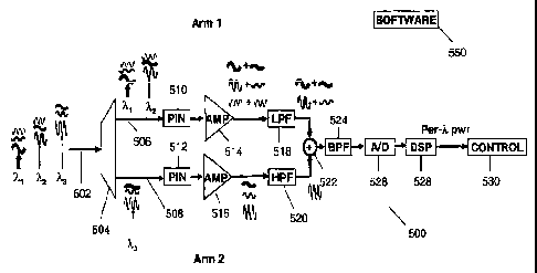
~U Figure 'rJ W1UW~3 r3la apparatus So0 for detecting am analr~rJt~R
~nc~iaatenanCe signal ire. accordance with a prRferred
embodiment o~ the prrrsent: inwPntion.
CA 02442375 2003-09-24
14
~rhe apparatus compra.~ps an. input BUG for receiV~.ng an
~hr.i rail signal cort~risina a plux'aliLy o~ c:~~amels , in the
exart~ple shown, the optical sig.c~al comprises three equally
spaced. c:ha.iuzeZ;~ at wavelengths A.1, ?.z and ~sj ( as described
S in relation to Figures 3 and 4).
The rQr_eivPC1 c-,pt-i ral signal is passed to a spliLGe.c 504.
Thp splitter acts to split zhe zwc;eived optical signal
ixito two bamd~; ut wavelength. in thi3 inotance, th~a two
so ba~~ds are rouo~hly of equal blocke of wavelength, w~_~:.h t-.hp
lower wavelength baz~d brainy prwi dPd via output 506 to~ Prxm
1 (510, 51a, 51B) , raTtCj rllP higher wavelength b~md being
pr~triaed via output 508 to Arm 2 (512, X26, 520) of the
detector.
Z5
Trx thin particular example, the first band Contains the
short wavaleru~th channel ~i finals at A1 and .?~z, and the
s2r_on.rl 'higher band Contains A~.
2D Lac:h d.ilu Of the dGteCtor COtnpx'scc~ a respective phoro-
detector 510, 5J.2 arranged to prnrl,~rc-! an output signal.
proportional to the tnta 1 power Of the iri'puC optical
si gr,a1 . FurtJler, each arm incorpox~a,te5 a filter Slfl, 520
arranged Lo pass substa=nt~.ally only the frequencicN of the
2S dxialugue maintenance signal3 withira the optica.~. band a.np»t
to the relevant arm. ~'or insta~n.ce, the ti rat-. arm has the
two lo~,rar wa~velcngt~h, s; finals As, ?~2. with respec:l.,ive
ana).~gmp mainvenance signals t~, ta. Txm low pass filter
513 is thus tirrariaed Lo pass L1 aiz:1 fz, but not pa.MC f3
30 1.e. ttte amaluguG mainterxatice sign.a.l of th,e chaxu~.el at A.3
(which is input to Aran 2) .
CA 02442375 2003-09-24
Sim~.larly, t-,hF hi gh pass E7.lLer 520 is arx'ay~d to pass
t3. but noL pass the lower Lt~c~u~zzcy ~snalogue maintenance
signals f~ and fz.
ror cOnvonicntse, each arm further r_~ntains ail electrical
am~,o~.ifier 514, 516, arranged to airiglify the output sic~mc~1
of t.hp respeCt;ive photo detector 510, X12 , p~ iox to irxput
to the filter.
s0 ~f vlssired, tfie outputs of each filter cam 1 c~ subse~xexitly
bo separatoly analysed r.~ c7caterml.ne Lhe separ3Le fz'ec~umloy
com~nnPnt~ present, and, the aFwli~udes of the frec~u.er~.cy
components. However, Lo zeduce costs, the preferred
eil~odim~il~ sh.~~wn in rigure 5 re-COmb~.nes the two omt~pi~t-.
15 signals ~rom t:he f~.lter~ 51.8. 520 by an adder 522 _
i
The output of 1-.hP adder 522 is vpY'ovided tc~ e~ band pass
filter, arranaed to pass all analogue mai,ntenaace
frequmc;y 5igizals, and to filter out: extremely lo~,r anr7
~x~r~mcly higl.a components that might be present. i n signal
(c:g. due to the informat:i_nrv hi. t.-rate) . 'This bcWd pass
filter 52d.: i s t:he ec~uivalenc filter to ~~m band pass
filter 250 Shown in F'ic~ux~ 1.
r'LS ~ per I~'igure: 1, the output of the band rasp i:i:Lter 524
can subccqueatly ba converted tn a di_git,al Signal by Lam
ar~,aloguQ to ~l i chi t-.a l converter' S2 b' . a7dd their Y.c ucessed by a
digital. sicTn,31 process~j 528 so as to dctcrmiae the
r
fr~queney CUIII~IU.~l~tl l.s present ( a . g . uwing Fast Fourier
Tra~,zsform pwocessing) . Subs~qu~antly, the frequency
coinponcntc presex~t and the ger ch~nnr~l. power Cal be passed
toy a r_ont.rnl unit 53U.
r
CA 02442375 2003-09-24
i
Thc~ control ur..it 530 can use this information to Control
the ~ perfnrmanoP nt at least one of : a node irsc;U~puraLii~g
fihp~detector; a link through whycxs n~ least a portion of
I
the; vptica~. ;dismal. has beers transmitted, ox will be
Lrasismitted subsequent to the analogue maintr~nax~.cP signal
I
measurement J:~cing made; or overall c-~ntrol of the
cor~s~.ectivity within the nPtworlc.
I
C:oznputer SoftiJare 550 may be used to implement contral
wittiirs l.he cvots;ol unit 530, and/or may ba used to contras I
the! detector 500, arsd/or pexform pa.x.t-. nt the Signal
proccccing within the dAter_.tnr 510 (e.g. Fourier asia,lvsi5
of ~ the P1 Pr1-.rical signal to determirse Lhe frequency
Coritponents prs;sent, a.ssc3 the amplitudes of ouch frequency
Component ) .
It 'will be appz'eeiatAd that the ahnvc~ apparatus d02S l7.ot
function so ac t-.n remove all of the ghost tvs~ee ref the
ease i oc~,~p mainvenarlce sic~xmls . 8owewer , i t doe3 ocrve to
~U rerctove those ~lmsl. tones originating from charirsels a
relatively lomg wavelength away from thp rPlavant ohanriC?1.
Corisequcntly, the accuracy of trR r3Ptected amplitude of
the xelevant anal ogv.e m3iriLenanCe tone i~ 5i~izifictxntly
i
i mprnvc?r1.
i
Il. ~ will also be appreciated that the abo~re amhndi.ment is
provided by way of example only, ~nc~ that vary-ous ways of
impl~amenting ~=he apr~ratus will be apparent tv l.he skilled
persn~ a~ telling within, the sc:u~e of the pre3cnt
3U invention.
ror inNtance, the splittar 5f74 has been d2soribed d5
cpl.a.tting thE: rer~?ivp~l AptiCal signal irsGu Lwo sepaiate
i
i
CA 02442375 2003-09-24
77
bands of wavel.enc~ths . S~~n'h a spl.itter Could be a coarse
Wavp~t pngth Diwisiori Multiplexer (oVDM) . IL clesized. the
splitter Coulc. be arranged to split. Lhe received optical
signal imtv l.~~L~~ o~: more separate bands of wavclongth.
Ire. the pre~e:cred embodiment , t~h. P ana l ogee mainteriar7.ce
sir~nal nn Par~li rh.annel has been referred to as d single
frp~,~pnc:y or gone. t'~owever, it will be dpp~~ciated that
analogue mainteimm~ sig~.mls might be pxovided by
1Q mudulaL,iazg eaclz chaxznal usit~.g a different modulation
format. for :.r~,stance one that wo~alc~ nr~:rupy a band of
frequencies r~.thpr tr,~n a single fregttency. It will also
hp apprPCiate~. that zhe present invemti,vm is applicable to
such modulation torma~s.
Whil9t the prcfez~red embodiment has hPaT ~7~scrib~ed with
reepect to or~:.y throe cha.nnpl ~ ( at-_ wavel~rl~L~7.s f 1~, . ?~~ and
?v.3) and rPSpective analogue maintenarlc;e 5i~nals (at
f rPC~uencies Ei . f? and :G~ ) , i I. wi 11 be apps eciated that the
2~ 'present inveza:.iuii voulJ. be implemented for anlr x~.umber of
cha.rix~,els . r;rcfarably, the splitter ar_ is fi~ split the
optical signal into r_nn.fi.irn~ous bands of wavelength, fox
exam~,l p a fiir:~t band including all c~L t~l~ lower wavelength
channels, and a second barra ilmluai~~y all of the higher
wavelengtxi cai<uulels. Preferably, the analogue mait~.texianr~Q
frequencies a:ee allocated to the channels sur_h i°hat-., once
the optical s:i.gnal has been split into bands, the analogue
maint.-.pnanr_P :signals fvr any band w~.zl tall within a
rr~spective~ r..on~overlappinq ra.rtye uL fzequencies. ThiN
facilitates L.Ll~~tiilg of the frequency o~.gnala.
Fi.guxe 6 sh~Tas an ex.~mr~ p where fox'ty Channels (dl.
wavelAnc~thc a~, J~3. A3. ....Aao) are utilised, each hnvirrg a
CA 02442375 2003-09-24
rp~pprt i vP .3n31ogue mdintenaxLCe frequenClr ( f~., ft, f3
...fao) . Fi,cfur~3 6 i11u5twctl.~~ l.~i~ wavwl~mgth plan i.e.
ouzpuc 506 of l.x~e 4VDM lilter cai~ be arranged to pass the
channels at wavelengths ?~1 ?~xo, whilEt output 509 of the
filter can be used to pass the chaxa..rP1 s at wa'crelengths
h2~,-- .~o . Ey a 7.7 y, t~hp 1 oar pass filter 5lti is arranaed to
pass analogue maintenance frequencies rl-LZO, and the high
pass filter 520 to pass Lz~~ueuci~s fZ~-f~o.
Alternati~src I,ow and high pass frequency plans, a.rd
splitter char acteri,st-.i r.s ran be used other than those
shown in r~igu:re ti. Fox instance, txae 5t~liLt~z need not
split the re~:eived optic:c~l 5i~na1 into two completel~r
Se,~araL~ ogti :al baryds . The splittcr merely needs to
1~ operate so tm to cn~ure that each portion of tha
respective signal from 1-ha ~p1 i rtc?r contains the maiority
ref th.P c~PSir~ci optical band, and a minority (i.e. less
than 501 .of the undesired optic:dl baii3(5) siyma2,
A~.z alteiriati~re embodimcz'~t of the present invention
utilises a fused fibre coupler. a:~ the sputter SUg. 'this
offers slightly reduced accuracy compared co a detec:Lct
incoxporatina a wavelenq, tPz c~i.vi5iom rnultiplexey , but at a
reduced cost.
Fuacd fibre couplers typically ha.vp a sinusoidal
transmittan,r~e h:?havi.ov.r with respect co waVelengtra. tai
the preferre6. embodiment, eac:x~. uutgut 50G, 5d~ of the
fused fibre c:ouplez~ i5 arrauyed to have full cxcuroion
across the total range o~ wavclengthe within the optir_'a1
signal. Fox- inetalzce, a typical band of wavPl.ength
utla.~.CRC~ t:C1 transmit optical siernals is Lhe C-bamc~ of
CA 02442375 2003-09-24
:19
Erhiaun, «i r.1, ~~hann~~l.s being arranged between wavelenctths
J.530 and 1560nm.
Figure 7 il.7.u~.~~d~e5 Llzc tzansmittance respoxme of a fucc
~ibx'e coupler acting ac a cplitter 504 for an optical
sigrzal containing only channels with.i n the ('.-hand. As can
be seen, thA first nLlt~mr. 5(7H o:h the splitter is arranged
to have a peak: LransmittanCe at Lhe low wavelezagLl~ eLlcl of
Lhe signal (153onrn) , aiic~ a luiuilnu,it't txaizsrnittance at the
high wavelerxgt;h end of the hand (1560nm) . with the otkzer
20 ov.tput 508 having a converse transmittance response.
Fiy .re ~ i 1 1 »=r_rar_es the wavelength and frec~uerac:y ~l~m fur
a..detector incorporating ouch a fused fibre coupler
splitter. Fow convenience, it i~ aacumed that each of the
.15 optical w.~vclc:ngthc has a respective analoc~uA mainl:.pnanr_p
frequ~ncy si0nal at a similarly increasing fregv,ency.
Cons2r~mntly t.ha 1nw 'pass ti.lter withii~ Arm 1 ConrieCLed Lo
OLttgtlL 50b Ot 'Che C011pler i5 dx~xcuy~~7. Lo pass the loMrex
LLwc.~uW lcy a~7.a.J-ague maintenance sigrs.a7..o~ whilEt the high
20 pass filter «~c~, the other arm is arranged to pass t-.hP
higher fre~xv.ez~cy analo~ap maintenance sicanals
corresponcla_z~c~ tn t-.hP .'Loner wave7.eiigth optical Channels.
=t will be i~~t~a Llzat in this ixrstance, there io come
2~ ovexlap betwc~~n the pace baz~.ds of the low pass fi l r.ar and
the high pass filter. This rwerlap i ~ provided so as Lo
compensate fnr r.hp fact that the coupler has a slowly
changing LxanamittanCe xesponse. HCwevcr, as this overlap
Occurs for analvcJ.u~ me.imL~naz~oe frec,~ue~a.cies corrcNponding
3o to channels having optical wavelex~gths close to the r-Pntrp
o~ the range of wavelengths used for t-.r~nsmi.ssion, then
these f..rpc~,~pnr~.iPS are relatively unaffected by SRS wlieiz
the wavelengtl2 band is fully u~ili5~~l.
CA 02442375 2003-09-24
Dine to thQ c~aupler and f. i.1 t-.pr nhar~rtpri stirs shown in
Figure 8, the analogue mainteriance tones received at ttie
~.xlput Lo Lhe digital sic~.znxl Ytuuesaut will have different
amplitudes even if all of the channclo arc of equal power
5 az~.d no SRS haE taken place . Tha lef t hand chart in Fic~urr~
9 shows the resulting reduction in ar_r_uraoy dmp t~ s»c~_'h
r.n»pl.er. and t filter characteristics . However, this error
is a fixed re~:ei'crer offset, and can ttaex~eluie Le currwl:ed
e.g. by using softv~tare, to give the accurate rccponoE
10 illustrated fir.. the right haxad eha.rt of Figure 9.
Figure 10 enoum a rnmperison between the l~red~.cted
accuracy of a conven'Cional analogue andizutemamc:c ~l~l.ectur
("uz'igiiial aw:uracy") , corresponding to performaxicc of a
15 detector has 'w~hOWn 1n Figure 1, and a detector as shown in
Figure 5 ("iz~proved accuracy") at different wavPlanQrhs.
This chart assumes that the ~nw pass and high pass filters
were fourth order c:hebyshev filters, and takes imLo
account i,h~ SRS glmst tone generation" the coupler
20 response, the filterixig attenuation and the phase. As can
be cecn, the original accuracy varies from approximately
. 3 to -1 _ SclES ar_rnss ~-k~.P c'.-har~r3 _ However, the pr'eseTlt
invention irlC~~eases the aCCUraCy of Lhe measux~e.~.uecm ut Llze
power pet wave:leriytlt ~uuh l.hal. the accuracy ahnre~ys remains
within the range 0.6 to 0.6d8.
Figure 1.1 provides performance prpc3i r_l~tons comparing 'the
original and in~roved analoGue maintenance det~c:tium
techniques fOr different SyStE.-'1Ll C:V11L1C~uratioms. In all
~:ases, the s~nc.ing between charmclo wac chosen such that
the chaz~nels covered the entire C-band. The graphs
aridicate for r~ar_h n»mhar of r_hannels, the max5.mum number
of ~panS Af optical fibre that maintain ttie aiialuc~.ua
CA 02442375 2003-09-24
maint.an~nc-p ~~~tpr.i-.i ~n ~r.rmrar_y within a predetermined
limit t 0 . 5db anc~ ldFS) . It swill also been seen t~ia.t by
u'tili~i.cx~ am ~YIIGtIUC~j.IlC lllCL111L1:11d11C:C twlmlquo in accordt~nC~
with the preee:nt in;rention, a grcatcr number of lengthE of
optical fibre wan utilised compared with the conventional
technique wh~.lst still maintaining a chi vPn 1 pv~'I nt
accuracy.
Tt will be apparent to the a7si11cd pcrwon that various
altcrziat~.vc analogue maintenance schemes, which split the
x~e_elved opti~-al signal into 1-wn or mnrp hanc3~ prior to
anainc~mp mairr.enance detection, will be understood as
falling wxth__n the scope of ' tx~e Y~wse~it it1V~11t1G11.
Figures 12--15 utilise identical reference ~nvmcrslo for
those componcmto that arc equivalent to tkze corresponding
components in the apparatus shown in Fir,~,.trP 5.
analogue maintenance detection apparatus 600 ,:~lUlNt1 111
f'l~ure 12 is ax-rangcd to ieceive a tap of an optical
s~' goal at input 502 . Epl.ittcr 504 oplits the optical
s.~'Zgnal into tin70 bands of equal blocks of ws.vRlAngth, wi.t.h
oil2 wavPlengt-h 1-»n~7 hPi ng provided by output 5U6 Lo a
f~ir5t input OE an optical switch 605, dmc~ tam vtlyer
Hiavelenytxa band Lily piuviJ,eJ. via output 50F3 to a second
input of the «ptica.l switch.
i
The optical scuitch 605 hay two inputs and a single output.
The switch 60~ is arranged to switch one of the ixaput5 ~o
the output, the output b~iy subset~ueiztly detected by
photo detecto__ 510. The photo detector 5~.0 i.s arranged to
~roducc are output signal proportional to the total power
r_rof the 1-ofi.al ~»w~r of the input optical sic~nal_ Hence, by
boggling the optical switch so as to direct ill l.urn the
CA 02442375 2003-09-24
22
t~o ban,r_1s. of barrel Pnc~t-.h t-.n i-.hP photo cYP~:ector, the photo
d lector can ~~eparately detect both th.e first band and the
second band.
Subsequez~txy, the rASUlting optical signal relatin7 to the
di tested optical band is amp11f1ed by PJ.er-t.ri c-al ampl i i~i.p'~'
51~, tilterea by band x~ass filtex 524 and converted to a
d~gitaZ siqna:. by analogue to digital eOraver 1. et 526 . lm
this particulaai ixzstance, the low pass filtoz'is~.g and the
hl gh pa33 filt:cring arc performed dig~.tal,ly by the digital
s~.gna2 processor 628.
1n the detection, apparatus 7D0 illustrated izx FiyuLe 13,
tizc two,bands of optical signal are separately detected by
respective photo dctcCtor~ 510, 513.
Ah eler_trir_al switch 7'f0 is arranged tn switch either the
a ectrical si~.~zla1 from photo Biode 57.0 or the electriedl
,5';LC.]Ilitll llUllt p7luLo dyodC 512 to the amplif~.er 51.x. IIence,
blur usixxg the :3witch to talcc altcrn3tc cample~e ~rom the two
I
photo diodes, and individually processing Pac->1 ef 1-.hP
s~c~n.als , an improved. ana 1 nc~,m ma i ntPnance deteCtiOn Cari be
p rformed. hgain, in this instance, the 1~w pe~.55
f ' ltering and ttie xli~I~ yeas Lil ~erimg (per formed by the
2~ f'lters; 51a, p20 in Figure 5) arc performed by the digital
~' final procoEe;or 628 .
Figures 14 aria, 15 show similar apparatus, in which each c,~
tlhe op'CiCSl bands from the spliLLe~ uuLp~xts 50G~ a08 are
s arately pr.oto detected, electrically amplified, band
p,ss filtcrcd and analogue to digitally converted_
CA 02442375 2003-09-24
1 the detection apparatus 800 ilyustx'ated in Figure 14, a
d~c~ital awi,Lc:h 827 ails l.v direct' either the digital
s~~-zal cerrespoading to the first band to the digital
olignal proccc:.or 62$, or the digital signal corresponding
ti th? secor:.~i ban.ri. t~n t.hp ~7i chi t-.a1 si final. processor 62ti .
Again, by togSTling the switch, altex'naLive samples can be
taken of each signal.
Ifs the appa,x'at:uc 900 illuotrated in Figure 15, the digital
si gns.l proces:~or 928 has taro inputs _ Thr~ digital s~_c,~na J
processor can be arranged to either process each o~ the
r puts in para11e1, ow a,lLe~ital,iv~l,y switch between the
izzputs ( 5u a;~ l.u ef ~ectively combine the operation of
dligital switars 82'7 and DEP 628 shown in Figuxe 14 ) . .
7~i-~ai", in hot=h the digital signal proCeSSOr 62$ Shown in
F' gate 14 anc, the digital sic_tnal processor 928 shuwzl :gym
Figure 15 , th~~ DSP dc; L s Lu per Lorni the low pas s f i1 tei ing
ald the high pass filtering.
.AnnthPr_ a~PP~a prr»ri c~.QS a method of offer7.xig a data
tI ansmission service over a network utilisizzy upLic:al
s' gnat. pruc:~:~si~y im accorcla~.ce With the present
iazventivn. As the advrantages of the invention can enable
a better r~,et~aork, eahich is more reliable, or m~ra
~lex~.ble, or having grPa.t-Pr r:apari.ty, or more Cost
ffeCtive for example, conseGuen~tJ.Y a data tz'azzsmussiul~
service ovax~ a izel,wuik ~:an show a corresponding
iV'yiUVerileilt. ~~~.~.J. the value of such services cats irzeresce.
ch i.ncrca~ed value over the life of the system, coulr_'l
rove far greater than the sales value o.f. t-.1~P pc~111 pment _
CA 02442375 2003-09-24
24
The reader's attention is directed to all papers and
documenLS whicrh are filed concurrently with oa~ previous to
this s~r~cifiCcaiVil i1~ cur~z~~ctzoxl with this application and
which arc open to public inspection with this
specification, and the contents c~f all such ropers and
cinri.~man,t~ arP inrnrpnrat-.P~7 hprE?in by rpfprpnrp_
A11 cat ttZe .Cecituz'e5 dlst;lUSed iii l.hi5 5,~~uiLiuaL1V11
( i7cicluding wtzy occompanyita,g cl,aimr, abstract and
1D dxawings), and/or all of the steps of an.y method or
rrncecs so ~3i ::r.__1 nsPC3, may hp rnmhinpd i n any nom.hination,
except combina3tions where at least some of such featuxes
andlor steps <<re xuutucr.l7.y exc:lu5ive.
Each feature discJ.osed in this specification (including
any acr_omranyir~g cJ.a.a.mc, ~~fost.r~r.t. anr7 drawings) , may YAP
rc~plar_Pd by alternative teatures serving the Swine,
equivalent or similar purpose, unless ~xpxwssly sts,tea
oth~~-vrise. Thos, unless ea,.-pxessly stated otherwise, each
fcaturc dioelnaod is one example only of a generic series
of Pc~.~ivalent or similar feat,_lrPS _
The invention is not restricted to txae aetail5 c1L Lhc
:~o:raguiilg ~1~1):~odizne~~t {s) . The invention e~Ctends to any
26 novel one, or any r~.oveJ. combination, of the ~eatures
disclosQd in this specification (inr_.luding any
~rr.nm~lan~ring r_laims, abstract and drawings) , or to ax~.y
novel one, ox any novel combination, of ttie steps ut ally
llll.-'~.11VC~ Vt ~JtVC:ejC~S S1.7 (~,.LSI:lOSCIa..