Note: Descriptions are shown in the official language in which they were submitted.
CA 02443616 2003-09-30
:kvava D. ..etNio. 502011-A-O1-i_J (Arnztt)
A COMMUNICATIONS CONNECTOR THAT OPERATES IN MULTIPLE
MODES FOR HANDLING MULTIPLE SIGNA.L. TYPES
TECHNICAL FIELD OF THE INVENTION
The present invention generally relates to communications connector
assemblies. More particularly, the present invention relates to a multi-
position
communications connector that is configured to operate in multiple modes for
handling multiple signals.
BACKGROUND OF THE INVENTION
Telecommunication equipment has benefited from the design of electrical
plugs and jacks that provide easy connect/disconnect capability between.
electrical
circuits within the telecommunications equipment and, for example, local
network
wiring. Such plugs and jacks are particularly popular in association with
telephone
sets, where they were first used, and, more recently, in association with a
large variety
of peripheral equipment that is connected to telephone lines. The modular
plugs and
jacks in use today have been standardized insofar as their performance
specifications
are concerned and also insofar as certain critical dimensions and structural
features are
concerned. The use of these devices has become so widespread that new houses
and
other buildings are pre-wired with jacks located throughout the various rooms,
as well
as in other strategic locations, to accommodate the communication equipment.
Where large numbers of such connections are needed, it is typical practice to
route the wires to a central location, such as a communication closet, where,
typically,
the jacks are mounted on patch panels. An example of such an arrangement is
disclosed in U.S. Pat. No. 5,096,439 of J. R. Arnett. In most installations,
it is
desirable that the jack be compact, and there have been numerous jacks
designed to
CA 02443616 2003-09-30
A.vaya Docket No. 502011-A-01-L'S (Arnett)
achieve this goal. For example, U.S. Patent No. 5,096,442 of J. R. Arnett
discloses
one such compact jack and plug arrangement, which together constitute a
compact
electrical connector. The compact electrical connector shown in that patent
includes a
metallic lead frame mounted to a spring block. The lead frame comprises a
number of
flat elongated conductors, each terminating in a spring contact at one end and
an
insulation displacement connector at the other end. The insulation
displacement
connectors are folded around opposite side walls of the spring block and
achieve
compactness, and the spring contacts are folded around the front surface of
the spring
block for insertion into a jack frame. The front surface of the spring block
includes a
tongue-like projection which fits into one end of the jack frame and
interlocks -
therewith.
The ability of connector assemblies to operate well at high frequencies is
limited by crosstalk within the assembly components, especially in the plug,
and as
frequencies increase, so does the limiting effect of crosstalk. In particular,
the rate of
data flow, which is ever increasing in communications, causes the wiring parts
to
become, in effect, antennae that both broadcast and receive electromagnetic
radiation.
This causes different pairs of wires to be electromagnetically coupled
together (i.e.,
crosstalk), which degrades the signal-to-noise ratio and increases error
rates.
Numerous arrangements have been proposed for reducing the effects of
crosstalk, including connector assemblies that are configured to minimize
crosstalk
and connector assemblies that comprise crosstalk compensating components in
the
overall circuit, such as additional capacitance in the jack for nullifying or
compensating for crosstalk in the plug. For example, U.S. Patent No. 5,186,647
of W.
J. Denkmann et al. discloses an electrical connector for conducting high
frequency
signals in which the input and output terminals are interconnected by a pair
of metallic
1
CA 02443616 2007-01-08
Avaya Docket No. 502011-A-01-US (Arnett)
lead frames mounted on a dielectric spring block. The lead frames, which are
substantially identical to each other, each comprise several flat elongated
conductors,
which terminate in spring contacts at one end and insulation displacement
connectors
at the other end. The conductors generally are parallel and close to each
other, but at
least one conductor of one frame is arranged to overlap at least one conductor
of the
other frame in a crossover region. As a result, the crosstalk between the
conductors is
reduced due to the reversal in polarities caused by the crossovers.
Notwithstanding these advances in dealing with crosstalk in connector
assemblies, an electrical connector having even less crosstalk would be
desirable.
It is also desirable to have a connector that is configured to make circuit
connections for uses other than crosstalk manipulation in order to provide a
greater degree of versatility. The connector assembly disclosed in the
aforementioned U.S. Patent No. 6,244,907, which is assigned to the assignee of
the present application, comprises a jack that is configured to mate with two
different types of plugs. A first one of the two types of plugs can be
inserted farther into the jack than the second one of the two types of plugs.
When the
first plug is mated with the jack, the contact wires on the plug abut free
ends of the
contact wires of the jack and cause the contact wires of the jack to deflect
toward and
come in contact with conductive pads on the wire board. The conductive pads
electrically connect the plug contact wires with compensation circuitry on the
wire
board, which has the effect of reducing crosstalk.
The second plug cannot be inserted as far into the jack as the first plug. The
contact wires of the second jack do not come into contact with the free ends
of the
jack contact wires, and so the free ends are not deflected onto the conductive
pads.
Hence, the compensation circuitry is not activated. Therefore, either the
3
CA 02443616 2003-09-30
Avaya Ducket No. 50201 1-r1-U1-US (Arnett)
compensation circuitry is on or off, depending on which type of plug is
inserted into
the jack, because either contact is made with the conductive pads or not.
Regardless of whether the compensation circuitry is activated or not, the
signal
path of the wire board is always the same, i.e., the signal path is never
through the
conductive pads and the compensation circuitry, but is always from the contact
wires
of the plug through the non-free ends of the contact wires of the jack (i.e.,
the ends
that are attached to the board). Consequently, regardless of the type of plug
that is
inserted into the jack, the sigrial path is always the same through the wire
board
circuitry.
A need exists for a communications assembly comprising a jack that is not
only capable of coupling with different types of plugs, but that is also
capable of
handling different signal types and of processing the signals in a manner
dictated by
the type of plug that is mated with the jack.
SUMMARY OF THE INVENTION
The present invention provides a jack that is configured to mate with at least
two different types of plugs. The jack comprises a wire board having first and
second
signal processing circuits thereon. When a first one of the different types of
plugs is
mated with the jack, the first signal processing circuit is activated. When a
second
one of the different types of plugs is mated with the jack, the second signal
processing
circuit is activated. The first signal processing circuit of the connector
assembly
includes crosstalk compensation circuitry for reducing or eliminating
crosstalk. The
second signal processing circuit of the connector assembly preferably does not
include
crosstalk compensation circuitry.
~
CA 02443616 2003-09-30
Avaya L,,.,xet No. 502011-a-01-L'S (Arnett}
Certain standard-compliant plugs exhibit a known amount of crosstalk and the
jacks with which the plugs are mated normally include crosstalk compensation
circuitry for eliminating or reducing the crosstalk. Because these standard-
compliant
plugs are still in wide use today, a need exists for a jack that is configured
to mate
with these plugs and that have circuitry for reducing or eliminating the
crosstalk in the
plugs. However, cables and plugs are currently being designed that exhibit no
crosstalk or only a small degree of crosstalk. Therefore, a need also exists
for a jack
that does not include crosstalk compensation circuitry. If a plug that
exhibits a certain
amount of crosstalk is mated with a jack that does not include crosstalk
compensation
circuitry, the connector assembly will not work properly. Similarly, if a plug
that does
not exhibit crosstalk is mated with a jack that includes crosstalk
compensation
circuitry, the connector assembly will not work properly.
The present invention provides a connector assembly comprising a jack that is
configured with a first signal processing circuit that includes crosstak
compensation
circuitry and with a second processing circuit that does not include crosstalk
compensation circuitry. This allows a single jack to be used with a low
performance,
standard-compliant plug that exhibits a certain level. of crosstalk as well as
with a high
performance plug that exhibits no, or very little, crosstalk.
The first and second signal processing circuits constitute separate signal
paths
on the wire board. Thus, when the first plug is inserted into the jack, the
signal is
operated on in accordance with the configuration of the first signal
processing
circuitry, and when the second plug is inserted into the jack, the signal is
operated on
in accordance with the configuration of the second signal processing
circuitry. Having
separate signal paths on the wiring board of the jack for each different type
of plug
ensures that the signal will be properly processed.
5
CA 02443616 2003-09-30
Avaya Docket No. 502011-A-O1-US (Arnett)
When the first plug is mated with the commi_rnications jack, a first conn-
.ctor
assembly is provided that compensates for crosstalk in the first plug. The
first plug
exhibits a predetermined level of crosstalk for whicli the first signal
processing circuit
is configured to compensate. When the secon.d plug is mated with tiie
communications jack, a second connector assembly is provided that does not
compensate for crosstalk. The second signal processing circuit does not
include signal
processing circuitiy because crosstalk is substantially absent from the second
plug.
These and other features and advantages of the present invention will become
apparent from the foliowing description, drawings and claims.
BRIEF DESCRIPTION OF THE DRAWINGS
Fig. I is a side view of the jack of the present invention in accordance with
the
preferred elnbodiment.
Figs. 2A and 2B are top views illustrating a first plug and a second plug,
respectively, mated with the jack shown in Fig. 1.
Fig. 3 is a side view of the jack shown in Fig. I inated with a plug of a
first
type.
Fig. 4 is a side view of the jack shown in Fig. 1 mated with a plug of the
second type.
2 0 Figs. 5A - 5F illustrate various views of examples of crosstalk
compensation
circuitry that may be included on the wiring board 11 of the present
invention.
6
CA 02443616 2003-09-30
Avava L, cket No. 502011-A-01-liS (A:-nett)
DETAILED DESCRIPTION OF THE PREFERRED EMBODIMENT
In accordance with the present invention, a communications connector
assembly is provided comprising a jack that is configured to mate with at
least two
plugs of different types. The jack comprises a wire board having at least two
different
sets of contacts. Each set of contacts is connected to a respective signal
processing
circuitry of the wire board. Thus, the wire board has at least two different
signal
paths, i.e., a separate signal path for each of the different plug types. The
signal path
that is activated at any given time depends on the type of plug that is mated
with the
jack. Consequently, the manner in which the signal. from the plug is processed
depends on the type of plug that is mated with the jack. -
One goal of the present invention that is met by the embodiment described
herein is eliminating moving parts in the connector assembly. By eliminating
moving
parts, the connector assembly is very robust and easy to assemble. Although
the
embodiment described herein is one arrangement that meets this objective, it
should
be noted that a variety of configurations could be derived from the principles
and
concepts of the present invention discussed herein. All of these
configurations are
within the scope of the present invention. In the interest of brevity, a
single
embodiment will be discussed. However, those skilled in the art will
understand from
the discussion provided herein that other configurations of the present
invention could
be designed using the principles and concepts demonstrated herein.
The present invention will now be described with reference to an example
embodiment of the present invention in which the jack is configured to mate
with two
different types of plugs. The first plug is a TIA/EIA-568 Common Building
Telecommunications Cabling Standard 568B plug (hereinafter "standard-
compliant"
plug). This particular plug is the most common type of plug found in
commercial
-7
CA 02443616 2003-09-30
Avaya Du,iet No. 502011 .a-0 1-L;5 (.arnett)
buildings. The TLa/EIA 568 standard specifies that the mated combination of
the
plug and jack must be at or below a certain crosstalk level. This type of plug
is
required to have a particular level of crosstalk, so the jack must be designed
to
compensate for this level of crosstalk. Other standard-compliant plugs would
also be
suitable for use with the jack of the present invention such as, for example,
a plug that
is compliant with the International Electrotechnical Commission (IEC) 60603-7
standard. The present invention is not limited to any particular types of
plugs.
When the first plug is mated with the jack of the present invention, the
contacts of the first plug deflect the contact wires of the jack onto a first
set of contact
posts on the wire board, which connect to a first signal processing circuit on
the wire
board. The first signal processing circuit includes crosstalk compenstion
circuitry that
compensates for crosstalk to ensure that the crosstalk of the mated
combination of the
jack and first plug is below the level specified by TLA/EIA standard 568.
The second plug is a high performance plug and is inserted farther into the
jack of the present invention than the first plug, as described in detail
below with
reference to Figs. 2A and 2B. For this plug, the jack does not require
crosstalk
compensation circuitry because the level of crosstalk in the plug is
relatively low in
comparison to the level of crosstalk exhibited by the first plug. When the
second plug
is mated with the jack of the present invention, the contact wires of the
second plug
deflect the contacts of the jack onto a second set of contact posts on the
wire board,
which connect to a second signal processing circuit on the wire board. The
second
signal processing circuit preferably does not include crosstalk compenstion
circuitry
because the crosstalk of the mated combination of the jack and second plug is
already
relatively low.
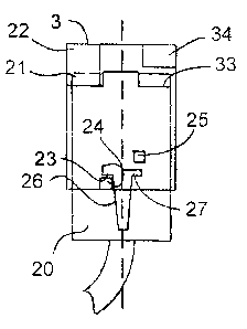
CA 02443616 2007-01-08
Avaya Docket No. 50201 1-A-01-US (Arnett)
Fig. 1 is a side view of the jack 1 of the present invention in accordance
with
the preferred embodiment. The jack 1 comprises a jack frame 2 having an
opening 3
formed in one end thereof for receiving a mating plug. The jack 1 comprises a
jack
wire assembly comprising jack contact wires 4 and a contact wire wrapping
mandrel
6, which is coupled to a cover (not shown) that is coupled to slots formed on
the
inside of the jack frame 2. A printed wire board (PWB) 5 is secured to the
jack 1.
The contacts wires 4 of the jack 1 are secured at first ends 7 thereof to the
wire board
5. The contact wires 4 have ends 7 that are affixed to the wire board 5 and
that wrap
around the mandrel 6 such that have free ends 8 of the contact wires 4 face
away from
the opening 3 formed in the jack frame 2 and are pre-loaded through abutment
with a
surface 9 of the jack 1 just above the free ends 8 of the contact wires 4.
The wire board 5 has a contact post assembly 10 attached to the upper surface
11 of the wire board 5. The contact post assembly 10 comprises a dielectric
base 12
and first and second rows 13 and 14 of contact posts. In accordance with this
example, each row 13 and 14 has eight contact posts. Therefore, the connector
assembly of the present invention in accordance with this embodiment is an 8-
contact-
wide assembly. Those skilled in the art, however, will understand from the
description provided herein that the connector assembly of the present
invention be a
6-contact-wide assembly, or any other number of contacts. The present
invention is
not limited to any particular number of contact posts or any particular type
of plug.
Also, the present invention is not limited to any particular number of rows of
contacts,
and thus is not limited with respect to the number of different types of plugs
that the
jack 1 can accommodate. For example, the wire board 5 could have three rows of
contact posts and three different signal processing circuits for processing
three
different types of signals.
9
CA 02443616 2007-01-08
Avaya Docket'.vo. 502011 _a-01-US (Arnett)
Figs. 2A and 2B are top views of the jack I of the present invention mated
with the first plug and the second plug, respectively. Fig. 2A depicts the
first plug 20
inserted into the jack frame 3 of the invention. It can be seen that rearward
movement
is limited by the shoulder of notch 21 engaging elongated plug stop member 22,
and
reverse movement is prevented by latching shoulder 23 of the latch 26 of the
first plug
20 engaging latching stub 24. As a consequence, plug 20 does not penetrate all
the
way into the jack frame 3, but, as will be seen clearly below with reference
to Fig. 3, it
does penetrate sufficiently into jack frame 3 to make the desired contact with
the row
14 of contact posts to create a low performance connection with the first
processing
circuitry (not shown) on the wire board 5 (Fig. 1). The manner in which this
occurs
can be seen in Fig. 3 and will be discussed below in detail with reference to
that
figure.
When the first plug 20 is inserted into the jack frame 3, it is inserted a
sufficient distance into the jack frame 3 to cause the latching shoulder 23 to
engage
the latching stub 24. The jack frame 3 has a second latching stub 25 that does
not engage the latching shoulder 27 of the latching tab 26 because of the
engagement
of the shoulder of notch 21 with the elongated plug stop member 22, which
prevents
further rearward movement (i.e., insertion) of the plug 20 within the jack
frame 3.
Fig. 2B depicts the second plug 30 inserted into the jack frame 3 of the
invention. The plug 30 is insertable into jack frame 3 until shoulder 31
engages plug
stop 22 and shoulder 33 engages plug stop 34. In this position, latching
shoulder 35
of the latching tab 36 latches to latch stub 25. In contrast to the latching
tab 26 of the
plug 20 shown in Fig. 2A, the latching tab 36 of plug 30 has a cutaway
straight side 37
that prevents the latching tab 36 from engaging latch stub 24. If this were
not the
case, then when that shoulder passed over stub 24, an installer might be
misled into
CA 02443616 2007-01-08
Avaya Docxet No. 502011 -A-0I-C;S (Arnett)
thinking the connection (i.e., mating) was complete, even though the plug 30
had not
been inserted sufficiently far into jack frame 3 for plug stops 34 and 22 to
engage plug
30. At the position of the plug 30 shown in Fig. 2B, the plug 30 penetrates
sufficiently into jack frame 3 (Fig. 4) to make the desired contact with the
row 13 of
contact posts to create a high performance connection with the second
processing
circuitry (not shown) on the wire board 5. The manner in which this occurs can
be
seen in Fig. 4 and will be discussed below in detail with reference to that
figure.
Fig. 3 is a side view of the connector assembly shown in Fig. 2A, wherein the
first plug 20 is fully inserted into the jack housing 3. At this position, the
latching
shoulder 27 on the side of the plug 20 has not engaged the latch stub 25, as
shown, but
the latching shoulder 23 (Fig. 2A) has engaged the latch stub 24 (Fig. 2A).
The
latching shoulder 23 and the latch stub 24 cannot be seen in the view shown in
Fig. 3
because they are on the side of the plug 20 opposite the side shown in Fig. 3.
At this
position, the free ends 8 of the jack contact wires 4 are deflected by the
plug blade 41
(the plug contact wires) downward away from the surface 9 of the jack housing
3 onto
the row 14 of contact posts, thereby establishing a connection between the
contact
wires of the plug 20 and the first signal processing circuit of the wire board
5. As
stated above, since the first plug 20 provides a particular level of crosstalk
that must
be compensated by the jack 1 of the present invention, the first signal
processing
circuit of the wire board 5 includes crosstalk compensation circuitry (not
shown) that
enables the signal from the plug 20 to be compensated for crosstalk.
Fig. 4 is a side view of the connector assembly shown in Fig. 2B, wherein the
second plug 30 is fully inserted into the jack housing 3. In this position,
the latching
shoulder 35 on the side of the plug 30 has engaged the latch stub 25, as
shown. The
latch stub 24 cannot be seen in the view shown in Fig. 4 because it on the
side of the
11
CA 02443616 2007-01-08
Avaya Docket No. 502011-A-01-US (Arnett)
plug 30 opposite the side shown in Fig. 4. At the position shown, the free
ends 8
of the jack contact wires 4 are deflected by the plug blade 51 (the plug
contact
wires) downward away from the surface 9 of the jack housing 3 onto the row 13
of contact posts, thereby establishing an electrical connection between the
contact
wires of the plug blade 51 of the plug 30 and the second signal processing
circuit
(not shown) of the wire board 5, which, in contrast to the plug 20 shown in
Fig. 3,
preferably does not include crosstalk compensation circuitry.
The differences between the physical structures of the first plug 20 and
the second plug 30 provide a keying mechanism that enables the jack 1 to
detect
the type of plug that has been inserted into the jack 1. These physical
configurations of the plugs and jack are disclosed in the aforementioned U.S.
Patent No. 6,244,907. It should be noted that the present invention is not
limited
to using this particular keying mechanism. This keying mechanism is preferred,
however, because the physical differences between the plugs also prevents
accidental insertion of the high performance plug 30 into a low performance
jack.
Figs. 5A - 5F illustrate various views of examples of crosstalk compensation
circuitry that may be included on the wiring board 11 of the present
invention. An
end view of printed wiring board 11 is shown in Fig. 5A, which has eight
layers of
wiring paths for introducing compensating crosstalk. Each of the layers
comprises
one or more metallic paths of thickness d, positioned on a dielectric material
of
thickness d2. The dimensions for di and d2 may be, for example, 0.04
millimeters
(mm) and 0.30 mm, respectively. In Fig. 5A, eight double-sided printed wiring
boards
601 - 605 are joined into a single unit 600 by epoxy layers in a manner known
in the
art. Each printed wiring board comprises a board material, such as FR-4, with
12
CA 02443616 2003-09-30
Avaya L,..Ket No. 502011-A-Ot-UJ (Arnett)
conductive paths pattemed on its top and bottom surfaces by standard
techniques such
as photolithography. While eight layers of signal paths are shown in this
illustrative
embodiment, it should be noted that any number can be employed.
Figs. 5B - 5F show top views of the wiring layouts on each of the layers of
the
printed wiring board l. In this example embodiment, the same wiring layout 43,
shown in Fig. 5D, is used on four layers of the wiring board. In this
particular
embodiment of the invention, the wiring layout of Figs. 5B - 5F provides three
stages
of compensating crosstalk between wire-pair 1(pins 4, 5) and wire-pair 2 (pins
3, 6),
which are identified in Fig. 5B (the industry generally refers to pins 3, 6 as
wire-pair
3). Fig. 5D shows discrete capacitors 62 connected between wire-pair 1 and
wire-pair
2 at the closest possible point to where signals enter layer 43 in the
jackwire terminal
region 65 of board 11, and they comprise the first stage of compensating
crosstalk.
While these discrete capacitors 62 comprise closely spaced wiring patterns on
a
printed wiring board, stand-alone discrete component structures could also be
used.
Additionally, although not immediately apparent from the wiring paths shown in
Figs.
5B, 5C, 5E and 5F, inductive coupling exists between wire-pairs 1, 2 in region
66 in
the form of closely spaced inductive loops that face each other. The self
inductance of
these loops improves the return-loss performance of the connector assembly,
while the
inductive coupling between these loops is part of the compensating crosstalk.
As
stated above, these crosstalk compensation circuits are only examples of
crosstalk
compensation circuits that can be used with the present invention.
It should be noted that the present invention has been described with
reference
to the preferred embodiments and that it is not limited to these embodiments.
Modifications, additions and/or deletions can be made to the embodiments
described
herein without deviating from the scope of the present invention. Those
skilled in the
13
CA 02443616 2003-09-30
Avaya Dvckettio. 502011-A-01-L S (Arnett)
art will understand in view of the discussion provided herein that all such
modifications, deletions and additions are within the scope of the present
invention.
For example, although the jack I is shown and described herein as having a
particular
design (e.g., contact posts arranged in two parallel rows on the wire board),
those
skilled in the art will understand in view of the disclosure that this design
is only one
of many possible designs for accomplishing the goals of the preseiit
invention. For
example, although the jack is described as having a first signal processing
circuit that
comprises crosstalk compensation circuitry and a second signal path that does
not, this
is not necessarily the case. The jack could instead comprise a first signal
processing
circuit could reduce crosstalk to a particular level and a second signal
processing
circuit that reduces crosstalk to a lesser amount.
The present invention has been described with reference to any croostalk
compensation being performed in the jack rather than in the plug. It should be
noted
that the concepts of the present invention equally apply to the plug. More
specifically,
the plug could be configured to have a latching arm that can be moved to, for
example, a first position and a second position. The second position would be
rearward of the first position to allow the plug to be inserted farther into
the jack.
Therefore, when the latching arm is in the first position, crosstalk
compensation
circuitry in the plug would not be activated and the plug would mate with the
jack in
the manner shown in Fig. 3 such that the crosstalk compensation circuitry in
the jack
would be activated. When the latching arrn of the plug is placed in the second
position, the plug would be inserted further into the jack and mate with the
jack in the
manner shown in Fig. 4. In this case, crosstalk compensation circuitry in the
plug
would be activated, but no crosstalk compensation would be performed in the
jack.
With such a plug, only one set of latching stubs would be needed on the jack.
14
CA 02443616 2003-09-30
Avaya DocKet No. 502011-A-01-US (?,.rnett)
Those skilled in the art will understand the many ways in which the concepts
of the
present invention may be implemented, and that all such implementations are
within
the scope of the present invention.