Note: Descriptions are shown in the official language in which they were submitted.
CA 02444149 2003-10-03
PULSE WAVE DETECTING APPARATUS AND F~URIEF; TRANSF~RM PR~CESS
APPARATUS
BACKGROUND ~F THE INVENTI:~N
Field of the Invention
The present invention relates to a pulse wave detecting apparatus having a
function of detecting a pulse wave of a subject, and also rates to a Fourier
transform
process apparatus that is suitable for the pulse wave detecting apparatus.
2. Description of the Related Art
Pulse wave detecting apparatus having a function of detecting a pulse wave of
a
IO subject have been developed. A pulse wave detecting apparatus has a
configuration in
which: a detecting section is attached to the body of a subject; a pulse wave
detected by
the detecting section is sampled; and signals resulting from the: sampling are
subjected to a
Fourier transform process to acquire vital information of the subject such as
the pulse rate
and blood pressure.
Methods of detecting a pulse wave include: a method i:n which a pulse wave is
detected using light; a method in which a pulse wave is detected by detecting
the pressure
of a blood stream with a piezoelectric element; and a method in which a pulse
wave is
detected by applying an ultrasonic wave generated by a piezoelectric element
to an artery
to detect a Doppler wave generated by a blood stream.
In any of the above-mentioned methods, a pulse signal acquired by a detecting
section is very small and susceptible to various noises such as noises
resulting from
movements of a bady (kinetic noises). This results in a problem in that it is
difficult to
acquire accurate vital information such as a pulse rate from a pulse wave
detected by the
detecting section.
CA 02444149 2003-10-03
A method for solving this problem is to reduce the influence of noises by
obtaining
moving averages of sampled signals. Such a method is described for example, in
Laid-
Open Japanese Patent Application JP-A-6-197891. According to this method,
since noise
components are leveled, the influence of noises can be reduced by performing a
Fourier
transform process on moving-averaged signals to acquire more accurate vital
information.
However, since the number of moving-averaged data i;~ equal to the number of
data
before the averaging, an increase in the number of data to be Fourier-
transformed increases
loads on a calculation unit to perform the Fourier transform.
Therefore, in the case of an apparatus such as a small apparatus having a
calculation unit with low calculating capability, a problem arises in that the
accuracy of
measurement is low because a sampling frequency cannot be set sufficiently
high.
It is an object of the invention to provide a pulse wave detecting apparatus
capable
of accurately measuring a pulse rate, even with a calculation unit having low
calculating
capability.
It is another object of the invention to provide a Fourier transform process
apparatus that is suitable for the pulse wave detecting apparatus.
SUMIvIARY OF THE INVENTION
The invention provides a Fourier transform processing apparatus, comprising: a
sampling process unit for sampling input signals at a first frequency and
sequentially
outputting resultant signals; an averaging process unit for sequentially
averaging a
predetermined number of signals from the sampling process unit and
sequentially
outputting resultant signals at a second frequency; and a Fourie:r transform
process unit for
performing a Fourier transform process on the signals from the averaging
process unit.
The sampling process unit samples input signals at a first frequency and
sequentially
outputs resultant signals. The averaging process unit sequentially averages a
predetermined number of signals from the sampling process unit and
sequentially outputs
2
CA 02444149 2003-10-03
resultant signals at a second frequency. The Fourier transform process unit
performs a
Fourier transform process on the signals from the averaging process unit.
A configuration may be employed in which the first frequency is n times the
second frequency (n being an integer equal to or greater than 2) and in which
the averaging
process unit averages every n signals from the sampling process unit in the
order of input
and sequentially outputs signals obtained through the averaging.
A configuration may be employed in which the second frequency is 2m Hz (m
being a positive integer).
The invention also provides a pulse wave detecting apparatus comprising: a
signal
detecting unit for detecting a pulse wave and outputting pulse signals
associated therewith;
a signal sampling process unit for sampling the pulse signals from the signal
detecting unit
at a first frequency and sequentially outputting resultant signals; an
averaging process unit
for sequentially averaging a predetermined number of signals from the signal
sampling
process unit and sequentially outputting resultant signals at a second
frequency; a signal
Fourier transform process unit for performing a Fourier transform process on
the signals
from the averaging process unit; and a pulse rate calculation process unit fox
calculating
a pulse rate based on the result of the process at the signal Fourier
transform process unit.
The signal detecting unit detects a pulse wave and outputs pulse signals
associated
therewith. The signal sampling process unit samples the pulse signals from the
signal
detecting unit at a first frequency and sequentially outputs resultant
signals. The averaging
process unit sequentially averages a predetermined number of signals from the
signal
sampling process unit and sequentially outputs resultant signals at a second
frequency.
The signal Fourier transform process unit performs a Fourier transform process
on the
signals from the averaging process unit. The pulse rate calculating process
unit calculates
a pulse rate based on the result of the process at the signal Fourier
transform process unit.
A configuration may be employed which includes: a noise detecting unit for
detecting kinetic noises and outputting noise signals associated therewith; a
noise
sampling process unit for sampling the noise signals from the noise detecting
unit at the
second frequency and sequentially outputting resultant signals; and a noise
Fourier
3
CA 02444149 2003-10-03
transform process unit for performing a Fourier transform process on the
signals from the
noise sampling process unit and in which the pulse rate calculation process
unit calculates
a pulse rate based on the signals output by the signal Fourier transform
process unit and
the noise Fourier transform process unit.
A configuration may be employed in which the first frequent;y is n times the
second frequency (n being an integer equal to or greater than Z) and in which
the averaging
process unit averages every n signals from the signal sampling process unit in
the order of
input and sequentially outputs signals obtained through the averaging.
A configuration may be employed in which the second frequency is 2m Hz (rn
being a positive integer).
BRIEF DESCRIPTI~N OF THE DRAWINGS'
Fig. 1 is a block diagram of a pulse wave detecting apparatus and a Fourier
transform process apparatus according to an embodiment of tree invention;
Fig. 2 is a waveform diagram for explaining a process in the embodiment of the
invention;:
Fig. 3 is a waveform diagram for explaining a process in the embodiment of the
invention;
Fig. 4 is a waveform diagram for explaining a process in the embodiment of the
invention;
Fig. 5 is a waveform diagram for explaining a process in the embodiment of the
invention;
Fig. 6 is a waveform diagram for explaining a process in the embodiment of the
invention;
Fig. 7 is a waveform diagram for explaining a process in a pulse wave
detecting
apparatus according to the related art;
Fig. 8 is a waveform diagram for explaining a process i:ra the embodiment of
the
invention; and
4
CA 02444149 2003-10-03
Fig. 9 is a waveform diagram for explaining a process in a pulse wave
detecting
apparatus according to the related art.
DESCRIPTION ~F TIDE (REFERRED EMBODIIvIENT
A preferred form of the present invention is illustrated in the accompanying
drawings in which:
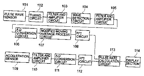
Fig. 1 is a block diagram of a pulse wave detecting apparatus according to an
embodiment of the invention.
In Fig. 1, the pulse wave detecting apparatus has a pulse wave sensor 101
provided
as a signal detecting unit that detects a pulse wave of a subject and outputs
pulse signals
associated therewith. A tuning circuit 102 extracts pulse signal components in
the signals
output by the pulse wave sensor 101. A filter and amplifier circuit 103
amplifies signals
having a predetermined frequency in signals output by the tuning
cia°cuit102 and allows
them to pass. A wave detection circuit 104 detects signals output by the
filter and amplifier
circuit 103. A filter and amplifier circuit 105 amplifies signals having a
predetermined
frequency among signals output by the wave detection circuit 104, and allows
them to
pass. An A-D conversion circuit 106 is provided as a signal sampling process
unit that
samples analog output signals from the filter and amplifier circuit 105 and
converts them
into digital signals. A modified maving average process circuit 107 is
provided as an
averaging process unit that performs an averaging process, as will be
described later on,
which signals output by the A-D conversion circuit 106. An FFT circuit 108 is
provided as
a signal Fourier transform process unit that performs a fast Fourier transform
(FFT)
process on signals from the modified moving average process circuit 107.
The pulse wave detecting apparatus also has an acceleration sensor 109
provided as a noise detecting unit that detects noises generated by movements
of the body
of a subject {i.e. kinetic noises) and outputs noise signals associated
therewith. A filter
and amplifier circuit 110 amplifies signals having a predetermined frequency
among the
signals output by the acceleration sensor 109 and allows them to pass. An A-D
5
CA 02444149 2003-10-03
conversion circuit I 11 is provided as a noise sampling process unit that
samples analog
output signals from the filter and amplifier circuit 1 I O and converts them
into digital
signals. An FFT circuit 112 is provided as a noise Fourier transform process
unit that
performs a fast Fourier transform (FFT) process on signals output by the A-D
conversion
circuit 111.
The pulse wave detecting apparatus has a pulse rate calculating circuit 113
provided
as a pulse rate calculation process unit that obtains a difference between a
signal output by
the FFT circuit 108 and a signal output by the FFT circuit 112. and calculates
a pulse rate
based on the difference signal. A display section 114 is provided as a display
unit that
displays the pulse rate calculated by the pulse rate calculation circuit 1 I3.
The pulse wave sensor 1 OI is used by attaching the same to the body (at a
wrist, for
example) of a subject to detect an arterial wave. Various sensors such as
optical sensors
and piezoelectric elements may be used depending on methods of detection. In
the case of
a method of detecting a pulse wave utilizing a Doppler effect of an ultrasonic
wave, the
pulse wave sensor 101 comprises a piezoelectric element for
t~.°ansmitting an ultrasonic
wave and a piezoelectric element for receiving an ultrasonic wave. In such a
case, an
ultrasonic wave transmission/reception circuit is used for transmitting and
receiving an
ultrasonic wave.
Further, the acceleration sensor 109 is used by attaching the same to the body
in
the vicinity of the pulse wave sensor 10I.
The A-D conversion circuit 106, the modified moving average process circuit
107,
and the FFT circuit 108 constitute a Fourier transform process apparatus.
Fig. 2 is a graph for explaining the process at the modified moving average
process
circuit 107. In Fig. 2, points Y0, Y1,Y2, and so on connected by a solid line
represent
signals that have been sampled and digitized by the A-D conversion circuit 106
and
signals output by the A-D conversion circuit 106. In the present embodiment, a
sampling
frequency of 16 Hz is used at the A-D conversion circuit 106, for example.
The modified moving average process circuit I07sequ~entially averages every
two
6
CA 02444149 2003-10-03
signals Y0, Y1, and so on output by the A-D conversion circuit 106 without
duplication
(the process being referred to as "modified moving average") to calculate and
output (Y0 +
Y1)/2, (Y2 -+- Y3)12, and so on. T'he modified moving average process circuit
107 outputs
digital output signals (YO + Y1)/2, (Y2 + Y3)/2, and so on having a frequency
(8 Hz in
S the present embodiment) that is one half of the sampling frequency of the A-
D conversion
circuit 106 as indicated by the broken line.
Fig. 3 shows signals output by the modified moving amerage process circuit
107.
Fig. 4 shows signals output by the FFT circuit 108. Fig. 5 shows signals
output by the A-
D conversion circuit 111. Fig. 6 shows signals output by the; FFT circuit 112.
Operations of the pulse wave detecting apparatus and the Fourier transform
process
apparatus according to the present embodiment will now be described in detail
with
reference to Figs. 1 to 6.
When attached to the body of a subject (at a wrist, for example), the pulse
wave
sensor 101 detects a pulse wave of the subject and outputs pulse signals
associated
therewith. The tuning circuit 102 extracts signals in the frequency range of
pulse signal
components from the signals output by the pulse wave sensor 101 and outputs
them. The
filter and amplifier circuit 103 amplifies signals having a predetermined
frequency
among the signals output by the tuning circuit 102 and allows them to pass.
The wave
detection circuit 104 detects the signals output by the filter and amplifier
circuit 103 and
outputs them to the filter and amplifier circuit 105. The filter and amplifier
circuit 105
amplifies signals having a predetermined frequency among the signals output by
the wave
detection circuit 104 and allows them to pass.
The A-D conversion circuit 106 samples analog output signals from the filter
and
amplifier circuit 105 at a predetermined frequency ( 16 Hz in the present
embodiment) and
converts them into digital signals that are output to the modified moving
average process
circuit 107. As shown in Fig. 2, the modified moving average process circuit
107
sequentially averages a predetermined number (two in the present embodiment)
of the
digital signals in the order of input without duplication and outputs signals
obtained
7
CA 02444149 2003-10-03
through the averaging to the FFT circuit 108. Thus, modified. moving average
signals
at 8 Hz are sequentially output by the modified moving average process circuit
107 as
shown in Fig. 3.
The FFT circuit 108 performs a digital Fourier transform (FfT) process on the
signals from the modified moving average process circuit 10 7 and outputs FFT-
processed
signals (FFT pulse signals) as shown in Fig. 4. The signals ~output by the FFT
circuit 108
include a base line corresponding to a pulse signal and base lines
corresponding to kinetic
noises, as shown in Fig. 4.
The acceleration sensor 109 that is attached to the body of the subject (at a
wrist,
for example) in the vicinity of the pulse wave sensor 101 detects movements of
the subject
and outputs kinetic noises associated therewith. The filter and amplifier
circuit 110
amplifies signals having a predetermined frequency among the signals output by
the
acceleration sensor 109 and allows them to pass.
As shown in Fig. 5, the A-I7 conversion circuit 111 samples analog output
signals
from the filter and amplifier circuit 110 at a predetermined frequency and
converts them
into digital signals that are output to the FFT circuit 112. In the present
embodiment, the
sampling frequency of the A-D conversion circuit 111 is set avt 8 Hz. That is,
the sampling
frequency of the A-D conversion circuit 106 is set at twice the; sampling
frequency of the
A-D conversion circuit 111. The sampling frequency of the ~A,-D conversion
circuit 11.1 is
set equal to the frequency of the signals output by the modified moving
average process
circuit 107, which makes it possible to easily reduce the influence of noise
components
such as kinetic noises when the pulse rate calculation circuit 113 calculates
a pulse rate.
The FFT circuit 112 performs a digital Fourier transfo~.-m (FFT) process on
noise
signals from the A-D conversion circuit 111 and outputs FFT-processed signals
(FFT
noise signals) as shown in Fig. 6. The signals output by the F'FT circuit 112
include no
base line corresponding to a pulse signal but include base lines corresponding
to kinetic
noises as shown in Fig. 6.
The pulse rate calculation circuit 113 obtains differences between the signals
output by the FFT circuit 108 and the signals output by the FFT circuit 112
(differences
CA 02444149 2003-10-03
between the signals in Figs. 4 and 6) to acquire signals associated with pulse
signals that
are less susceptible to noises such as kinetic noises. Next, the pulse rate
calculation
circuit 113 calculates the pulse rate of the subject based on a center
frequency of the
signals thus obtained and outputs a signal indicating the pulse rate to the
display section
S 114. The display section 114 displays the pulse rate.
When the modified moving average process circuit 107 is deleted as in the
pulse
wave detecting apparatus according to the related art, the FFT circuit 108
outputs signals
as shown in Fig. 7.
Let us compare the signal-to-noise ratios in Figs. 4 and 7 based on the
definition
that a signal-to-noise ratio equals the sum of the heights of base lines
corresponding to
pulse signals and the heights of base lines before and after the. same divided
by the sum of
the heights of all base lines. Then, the signal-to-noise ratios in Figs. 4 and
7 are 0.145 and
0.123, respectively. Thus, the present embodiment including the modified
moving
average process circuit 147 provides a signal-to-noise ratio better than that
of the pulse
wave detecting apparatus according to the related art and allows highly
accurate
measurement by suppressing the influence of noises. Since the use of the
modified
moving average process circuit 107 makes it possible to reduce the number of
data to
be processed, loads on the Fourier transform circuit 108 and the pulse rate
calculation
circuit 113 can be reduced.
As described above, the pulse wave detecting apparatus of the present
embodiment
is characterized in that it has the pulse wave sensor 101 that detects a pulse
wave of a
subject and outputs pulse signals associated therewith, the A-D conversion
circuit 106 that
samples the pulse signals from the pulse wave sensor 101 at a first
predetermined
frequency and sequentially output s resultant digital signals, the modified
moving average
process circuit 107 that sequentially averages a predetermined number of
digital signals
from the A-D conversion circuit 106 and sequentially outputs resultant signals
at a second
predetermined frequency, the Fourier transform circuit 108 that performs a
Fourier
transform process on the digital signals from the modified moving average
process circuit
9
CA 02444149 2003-10-03
107, and the pulse rate calculation circuit 113 that calculates a pulse rate
based on the
result of the process at the Fourier transform circuit 108. Thus, since the
signals are
averaged by the modified moving average process circuit 107, highly accurate
measurement can be earned out with the influence of noises being suppressed.
Further,
since the number of data to be processed can be reduced, a, pulse .rate can be
more
accurately measured even when the calculating unit such a.s the Fourier
transform circuit
108 and the pulse rate calculation circuit 113 has low calculating capability.
The pulse wave detecting apparatus of the present embodiment is also
characterized in that it has the acceleration sensor 109 that detects kinetic
noises and
outputs noise signals associated therewith, the A-D conversion circuit 111
that samples
the noise signals from the acceleration sensor 109 at the second frequency and
sequentially
outputs resultant signals, and the Fourier transform circuit 112 that performs
a Fow-ier
transform process on the signals from the A-D conversion circuit 11 I and in
that the pulse
rate calculation circuit 113 calculates a pulse rate based on the signals
output by the
Fourier transform circuits 108 and 112. Thus, even when kinetic noises are
generated by
movements of a subject, the influence of the noises can be suppressed to allow
highly
accurate measurement.
The Fourier transform process apparatus of the present embodiment is
characterized in that it has the A-D conversion circuit 106 that samples input
signals at a
first frequency and sequentially outputs resultant digital signals, the
modified moving
average process circuit 107 that sequentially averages a predetermined number
of digital
signals from the A-D conversion circuit 106 and sequentially outputs resultant
signals at a
second frequency, and the Fourier transform circuit 108 that performs a
Fourier transform
process on the signals from the modified moving average process circuit 107.
Therefore,
a more accurate Fourier transform process can be carried out even when the
Fourier
transform circuit 108 has low calculating capability, which makes it possible
to provide
a Fourier transform process apparatus suitable for a pulse wave detecting
apparatus that
must be small-sized and capable of measuring a pulse rate accurately.
CA 02444149 2003-10-03
A configuration may be employed in which the first frequency is n times the
second frequency (n being an integer equal to or greater than 2) and in which
the modified
moving average process circuit 107 sequentially averages every n signals input
from the
A-D conversion circuit 106 and sequentially outputs signals obtained through
the
averaging. A configuration may be employed in which the second frequency is 2m
Hz (m
being a positive integer). This allows the FFT circuit 108 to perform its
process
quickly.
The modified moving average process circuit 107, the FFT circuits 108 and 112
and the pulse rate calculation circuit 113 may be constituted by a central
processing unit
(CPiU).
When the pulse rate of a subject may be statically identified without
consideration
to movements of the subject, the acceleration sensor 149, the filter and
amplifier circuit
110, the A-D conversion circuit 111, and the FFT circuit 112 are not required
and, in this
case, the pulse rate calculation circuit 113 calculates the pulse rate based
on signals from
the FFT circuit 108.
Figs. 8 and 9 are waveform diagrams for explaining a process of identifying a
pulse rate statically. Fig. 8 is a waveform diagram of signals that are
statically obtained
from the FFT circuit 108 of the pulse wave detecting apparatus in Fig. 1. Fig.
9 is an output
waveform diagram of an FFT circuit of a pulse wave detecting apparatus
according to the
24 related art which does not have the modified moving average process circuit
107.
Let us define that a signal-to-noise ratio equals the sun of the heights of
base lines
corresponding to pulse signals and the heights of base lines before and after
the same
divided by the sum of the heights of all base lines, just as mentioned above.
Then, signal-
to-noise ratios of 0.24 and 0.21 result from Figs. 8 and 9, respectively.
Thus, the present
embodiment including the modified moving average process circuit 107 provides
a signal-
to-noise ratio better than that of the pulse wave detecting apparatus
according to the
related art and allows highly accurate measurement by suppressing the
influence of
noises.
11
CA 02444149 2003-10-03
The pulse wave detecting apparatus according to the invention allows more
accurate measurement of a pulse rate even with a calculation unit having low
calculating
capability.
Further, the invention makes it possible to provide a Fourier transform
process
apparatus suitable for the pulse wave detecting apparatus that is capable of
more accurate
measurement of a pulse rate even with a calculation unit having low
calculating capability.
12