Note: Descriptions are shown in the official language in which they were submitted.
CA 02445715 2003-11-03
- 1 -
INTERLEAVING/DEINTERLEAVING DEVICE AND METHOD FOR
COMMUNICATION SYSTEM
BACKGROUND OF THE INVENTION
1. Field of the Invention
The present invention relates generally to a communication system, and in
particular, to an interleaving/deinterleaving device and method for a radio
communication system.
2. Description of the Related Art
Interleaving is typically used in mobile communications to increase the
performance of an error correction code in a fading channel, and is intimately
associated with decoding of a random error correction code. Particularly, an
air
interface for an IMT-2000 communication system requires a concrete method for
implementing various interleaving techniques. In addition, the methods for
interleaving have resulted in an increase in the reliability of digital
communication
systems, and in particular, have resulted in a performance improvement for
existing
and future digital communication systems alike.
The IMT-2000 standard provisionally recommends using a bit reverse
interleaver for a channel interleaver. However, the forward link and the
reverse link
defined by the IMT-2000 standard have various types of logical channels, and
the
interleaver has various sizes. Therefore, in order to solve this variety
requirement,
there is required the increased memory capacity. For example, in a N=3 forward
link
transmission mode, there is used an interleaver of various sizes from 144
bits/frame to
36864 bits/frame. A brief description of the bit reversal interleaver will be
made
below.
FIG. 1 shows a permutation method of the bit reversal interleaver. Referring
to FIG. 1, the bit reversal interleaver rearranges frame bits by exchanging
bit positions
CA 02445715 2003-11-03
-2-
from the most significant bit (MSB) to the least significant bit (LSB),
thereby to
generate an interleaving address. This interleaving method has the following
advantage. Since the interleaver is implemented using an enumeration function,
it is
simple to use the memory and it is easy to implement interleavers of various
sizes. In
addition, the bit positions of the permuted sequence are distributed at random
in major
locations. However, an interleaver having a size which cannot be expressed in
terms
of a power of 2 has a reduced memory efficiency. For example, to implement the
36864-bit interleaver, there is required a 64Kbit (65536=216) memory. Since
the value
36864 is higher than 32Kbits (32768= 215) an additional bit is needed to
represent the
number. Therefore, 28672 (=65536-36864) bits are unused in the memory, thereby
causing a memory loss. In addition, even though the memory has a sufficient
capacity,
it is very difficult to implement a method for transmitting the symbols.
Further, it is
also difficult for the receiver to detect an accurate position of the received
symbols.
Finally, since various types of interleavers are used, it is necessary to
store various
interleaving rules -in memory thereby requiring a controller (CPU) to have a
high
memory capacity as well.
The conventional interleaving method has the following disadvantages. First,
in the existing interleaving method, the size of the interleaver cannot be
expressed in
terms of a power of 2, and the interleaver having the larger size is less
memory
efficient. That is, in most cases, the size of each logical channel is not
expressed in
terms of 2' , therefore the interleaver has a large size when designing an
interleaver for
the IMT-2000 forward link. Therefore, it is ineffective to use the bit
reversal
interleaving method.
Second, in the existing interleaving method, it is necessary to store various
interleaving rules according to the interleaver sizes in the controller (CPU
or host) of
the transceiver. Therefore, the host memory requires a separate storage in
addition to
an interleaver buffer.
Third, the interleaver/deinterleaver has a complex transmission scheme
because invalid address should be removed when the interleaver size is set to
2' to
perform bit reversal interleaving. Further, the interleaver/deinterleaver has
difficulty in
synchronizing the symbols.
,
CA 02445715 2004-09-16
75998-108D
-3-
SUMMARY OF THE INVENTION
It is, therefore, an object of the present
invention to provide an interleaving device and method for
generating an address for various interleaver sizes using a
single algorithm in a communication system.
It is another object of the present invention to
provide an interleaving device and method for allowing an
interleaver memory to use only a capacity corresponding to a
frame size N in a communication system.
To achieve the above objects, there is provided a
device for sequentially storing input bit symbols of a given
interleaver size N in a memory at an address from 0 to N-1
and reading the stored bit symbols from the memory. The
device comprises a look-up table for providing a first
variable m and a second variable J satisfying the equation
N=2mxJ; and an address generator for generating a read
address depending on the first and second variables m and J
provided from the look-up table. The read address is
determined by 2m(K mod J)+ BROm(K/J), where K(0<_K<_(N-1))
denotes a reading sequence, BROm(y) is the bit-reversed m-bit
value of y and / is a function in which a quotient of K
divided by J is obtained, the quotient being an integer.
There is also provided a method for sequentially
storing N input bit symbols in a memory at an address from 0
to N-1 and for reading the stored bit symbols from the
memory, comprising the steps of: providing a first variable
m and a second variable J satisfying the equation N=2mxJ; and
reading a Kth(0<_K<_(N-1)) bit symbol at an address determined
by 2m(K mod J)+ BROm(K/J) where BROm(y) is the bit-reversed
I I I
CA 02445715 2004-09-16
75998-108D
-3a-
m-bit value of y and / is a function in which a quotient of
K divided by J is obtained, the quotient being an integer.
There is further provided a method for
sequentially storing input bit symbols of a given
interleaver size N in a memory at an address from 0 to N-1
and reading the stored bit symbols from the memory, wherein
a bit symbol is read at an address determined by the
equation 2m x r + s, wherein when the interleaver size N is
expressed as a binary value, an integer equal to or smaller
than the number of consecutive zero bits from the LSB is
defined as a first variable m, a decimal value determined by
converting a binary value corresponding to the truncated
bits other than the consecutive zero bits is defined as a
second variable J, a decimal value determined by expressing
a quotient obtained by dividing a reading sequence
K(0:5KS(N-1)) by the second variable J, as a binary value
with m bits bit reversing said binary value and converting
the bit-reversed binary value to said decimal value is
defined as a fourth variable s, and a remainder determined
by dividing the reading sequence K by the second variable J
is defined as a third variable r, the quotient being an
integer.
There is still further provided a device for
interleaving an input bit symbols, the device comprising:
memory to store the input bit symbols of a given interleaver
size N at an address from 0 to N-1; and an address generator
to generate a read address depending on a first-and second
variables m and J provided from the memory, the read address
being determined by 2m(K mod J)+ BROm(K/J) where the first
and second variable m and J satisfying the equation N=2mxJ,
K(0<_K<_(N-1)) denotes a reading sequence, BROm(y) is the
CA 02445715 2004-09-16
75998-108D
-3b-
bit-reversed m-bit value of y and / is a function in which a
quotient of K divided by J is obtained, the quotient being
an integer.
There is still further provided a device for
sequentially storing input bit symbols of a given
interleaver size N in a memory at an address from 0 to N-1
and reading a bit symbol stored at an address R from the
memory, the device comprising: means for providing a first.
variable m and a second variable J satisfying the equation
N=2mxJ; and means for generating a read address depending on
the first and second variables m and J provided from the
providing means, the read address being determined by
2n'(K mod J)+ BROm(K/J) where K(0<_KS(N-1)) denotes a reading
sequence, and BROm(y) is the bit-reversed m-bit value of y
and / is a function in which a quotient of K divided by J i_s
obtained, the quotient being an integer.
BRIEF DESCRIPTION OF THE DRAWINGS
The above and other objects, features and
advantages of the present invention will become more
apparent from the following detailed description when takeri
in conjunction with the accompanying drawings in which:
FIG. 1 is a diagram for explaining a permutation
method of a bit reversal interleaver according to the prior
art;
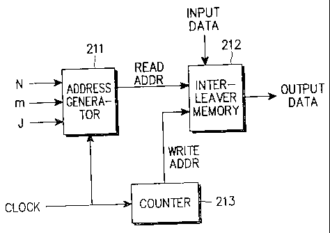
FIG. 2 is a block diagram of an interleaver
according to an embodiment of the present invention; and
FIG. 3 is a block diagram of a deinterleaver
according to an embodiment of the present invention.
CA 02445715 2004-09-16
75998-108D
-3c-
DETAILED DESCRIPTION OF THE PREFERRED EMBODIMENT
A preferred embodiment of the present invention
will be described herein
CA 02445715 2004-09-16
_4_
below with reference to the accompanying drawings. In the following
description,
well-known functions or constructions are not described in detail since they
would
obscure the invention in unnecessary detail.
An interleaver/deinterleaver according to an embodiment of the present
invention permutes the sequence of input symbols using an
interleaving/deinterleaving
algorithm - and then stores them in an output buffer in a new sequence.
Therefore, the
interleaver/deinterleaver proposed by the invention comprises three parts: an
interleaver memory (input data buffer and output data buffer), an address
generator,
and an existing counter.
FIG. 2 shows an interleaver according to an embodiment of the present
invention. Referring to FIG. 2, an address generator 211 receives an
interleaver size
value N, a first variable m, a second variable J and a clock, to generate an
interleaver
memory address for reading bit symbols sequentially stored in an interleaver
memory
212. The interleaver memory 212 sequentially stores input bit symbols during a
write
mode of operation, and outputs the bit symbols according to the address
provided
from the address generator 211 during a read mode of operation. A counter 213
counts
the input clock and provides the clock count value to the interleaver memory
212 as a
write address value.
As described above, the interleaver sequentially writes the input data during
the write mode of operation, and outputs the data stored in the interleaver
memory 212
according to the read address generated from the address generator 211.
Here, the address generator 211 generates the read address (i.e., interleaving
address value) according to a partial bit reversal interleaving algorithm
defined by
Equation (1) below.
[Equation 1]
ForagivenK..... (05KS(N-1))
r=KmodJ;
PUC=K/J;
S= BROm(PUC);
ADDRESS READ = r x 2r"+s
CA 02445715 2004-09-16
75998-108D
-5-
where 'K' denotes the sequence of output data bits and is
referred to as a sequence number; 'm' denotes the number of
consecutive zero (0) bits from the LSB to the MSB and is
referred as a first variable; and J denotes a value
corresponding to a decimal value of the bits except the
consecutive zero (0) bits (i.e. m) and is referred to as a
second variable. Here, the interleaver size N is defined as
2mxJ.
A description will now be made regarding a method
of generating the address for reading the input symbols
sequentially written in the memory, with reference to
Equation (1). Assume that the size of the interleaver is N.
In Equation (1), K(=0,1,2,===, N-1) indicates a reading
sequence of the input data, and r, PUC, s indicate
predetermined variables. Further, 'mod' and '/' indicate
each modulo operation and divider operation for calculating
the remainder and quotient, respectively. As it would be
obvious to a person of ordinary skill in the art, the terms
'mod' in a modulo operation for calculating a remainder and.
'/' in a divider operation for calculating a quotient occur
in the context of the quotient-remainder theorem where a
remainder r and a quotient q are integers satisfying the
relationship n=dxq+r, where 0 S r < d. In addition, BROn,(H)
indicates the bit-reversed m-bit value of H - the process
involving converting 'H' to a binary value and then
converting it to a decimal value by reverse ordering the
binary value from the MSB to the LSB. The resulting decimal
value is the value representing the bit reversed binary
value. Therefore, by using the function of Equation (1),
the interleaver may calculate the read sequence index
ADDRESS READ corresponding to 'K' of the input data sequence
and read the contents of the memory according to the read
, , , .
, i ,
CA 02445715 2004-09-16
75998-108D
-5a-
sequence index ADDRESS_READ. The first and second variable:;
are determined by the interleaver size. Once the
interleaver size N and the first and second variables are
determined, the interleaver generates, depending on these
values, a new addressing index ADDRESS_READ corresponding to
each K according to the following algorithm, and reads the
data from the interleaver memory 212 using the addressing
index ADDRESS READ.
A description will now be made regarding a method
for determining the first and second variables from the
frame size (or interleaver size) N. A predetermined
interleaver size N is expressed as a binary value. Further,
the number of consecutive '0' bits which continue from the
LSB to the MSB is calculated and then defined as first
variable m. Thereafter, the truncated bits other than the
consecutive zero bits are assembled and converted to a
decimal value. The converted decimal value is defined as
the second variable J.
For example, when N=576, it can be converted to a
binary value of N=[10 0100 0000], so that m=6 and
J=(1001)2=9.
CA 02445715 2003-11-03
-6-
FIG. 3 shows a deinterleaver having a reverse operation of the above
interleaver.
Referring to FIG. 3, an address generator 311 generates a deinterleaver
memory address for performing a write mode of operation by receiving an
interleaver
size value N, a first variable m, a second variable J and a clock. Address
generator
311 provides the generated deinterleaver memory address to a deinterleaver
memory
312. The deinterleaver memory 312 stores input data according to the write
address
provided from the address generator 311 during a write mode of operation, and
sequentially outputs the stored data during a read mode of operation. A
counter 313
counts the input clock and provides the clock count value to the deinterleaver
memory
312 as a read address value.
The deinterleaver has the same structure as the interleaver and has the
reverse
operation of the interleaver. That is, the deinterleaver is different from the
interleaver
in that input data is stored in the deinterleaver memory 312 using the
algorithm of
Equation (1) during the write mode of operation, and the data is sequentially
read
during the read mode of operation. That is, the deinterleaver stores the data
in the
original sequence during the write mode in order to restore the original
sequence of
the data transmitted from the transmitter.
For convenience, the description below will now be made with reference to
the interleaver. The reference will be made to an embodiment which is applied
to the
IMT-2000 system being a further mobile communication system.
First, with reference to Table 1 below, a detailed description will be made
regarding the interleaver size used in the forward link of the IMT-2000
system.
[Table 1]
F-FCH F-FCH F-SCH F-SCH F-CCCH F-SYNC F-PCH F-DCCH
(RS 1) (RS2) (RS 1) (RS2) CH
CA 02445715 2003-11-03
-7-
72 (bit)
144 0 0 0
(5msec) (5msec) (5msec)
192 0
(26.6msec)
288
384
576 0 0 0 0 0 0 0
(20msec)
1152 0 0 0
2304 0 0
4608 0 0
9216 0 0
18432 0 0
36864 0 0
CA 02445715 2003-11-03
-g-
where F-FCH stands for a forward fundamental channel, F-SCH for a forward
supplemental channel, F-CCCH for a forward conunon control channel, F-SYNC CH
for a forward sync channel, F-PCH for a forward paging channel, and F-DCCH for
a
forward dedicated control channel.
It is noted from Table 1 that in the IMT-2000 system, there are proposed 12
interleaver sizes (N=12) each applied to the forward logical channels as
indicated by
'0'. For example, a forward fundamental channel F-FCH (for Rate Set 2) uses
144-bit,
576-bit and 1152-bit interleaver sizes, wherein a 5ms frame is used for the
144-bit
interleaver size.
Shown in Table 2 below are the first variable m and the second variable J
calculated for the interleaver sizes of Table 1.
[Table 2]
Interleaver Binary Value for N J m Logical Channel
Size (N)
144 10010000 9(1001) 4 5msec/frame
F-DCCH (5msec/frame)
F-FCH/RS2 (5msec/frame)
192 1100000 3(0011) 5 F-SYNC CH (26.22msec/frame)
576 1001000000 9(1001) 6 F-PCH
F-CCCH
F-DCCH (20msec/frame)
F-FCH/RS2
F-SCH/RS 1
1152 10010000000 9(1001) 7 F-FCH/RS2
F-SCH
2304 100100000000 9(1001) 8 F-SCH
4608 1001000000000 9(1001) 9 F-SCH
9216 10010000000000 9(1001) 10 F-SCH
18432 100100000000000 9(1001) 11 F-SCH
36864 1001000000000000 9(1001) 12 F-SCH
With reference to Table 2, a description will be made regarding a method for
calculating the first and second variables for the interleaver size of N=9216.
First, the
interleaver size 9216 can be expressed as a binary value of N= [10 0100 0000
0000].
For this binary value, the maximum number of consecutive zero (0) bits from
the LSB
to the MSB is calculated, and then the calculated value is defined as the
first variable
CA 02445715 2003-11-03
-9-
m. Thereafter, the truncated bits other than the consecutive zero bits are
assembled
and converted to a decimal value (1001=9(1o)). This decimal is called the
second
variable J.
Tables 3 and 4 below show the write and read modes for N=576 interleaver,
respectively, by way of example.
[Table 3]
1 2 3 4 5 6 7 8 9 10
11 12 13 14 15 16 17 18 19 20
21 22 23 24 25 26 27 28 29 30
31 32 33 34 35 36 37 38 39 40
41 42 43 44 45 46 47 48 49 50
51 52 53 54 55 56 57 58 59 60
61 62 63 64 65 66 67 68 69 70
71 72 73 74 75 76 77 78 79 80
81 82 83 84 85 86 87 88 89 90
91 92 93 94 95 96 97 98 99 100
541 542 543 544 545 546 547 548 549 550
551 552 553 554 555 556 557 558 559 560
561 562 563 564 565 566 567 568 569 570
571 572 573 574 575 576
[Table 4]
1 65 129 193 257 321 385 449 513
33 97 161 225 289 353 417 481 545
17 81 145 209 273 337 401 465 529
49 113 177 241 305 369 433 497 561
9 73 137 201 265 329 393 457 521
41 105 169 233 297 361 425 489 553
25 89 153 217 281 345 409 473 537
57 121 185 249 313 377 441 505 569
CA 02445715 2004-09-16
75998-108D
-10-
69 133 197 261 325 389 453 517
16 80 144 208 272 336 400 464 528
48 112 176 240 304 368 432 496 560
32 96 160 224 288 352 416 480 544
64 128 192 256 320 384 448 512 576
In the write mode of operation, the input data
bits are sequentially stored in the interleaver memory 212
from an address 000 to an address 575, as shown in Table 3
5 which shows the corresponding orders 1 to N of the address 0
to N-1. Next, in the read mode of operation, the data bits
are output from the interleaver memory 212 using the read
address generated from the address generator 211.
As an example, for a third output data bit (k=2),
a calculation of a corresponding read address will be
described with reference to Equation (1). First, for N=576,
m=6 and J=9. Therefore, r=2 mod 9=2, and PUC= 2/9=0. In
addition, s=BRO6(0)=0. As a result, the finally calculated
read address ADDRESS READ=2x26=128. In the read mode of the
interleaver as shown in Table 4 corresponding orders of the
output addresses are shown as 1 to N. That is, all output
addresses obtained from Equation (1) are added by 1,
respectively.
As an another example, for a 20th output data bit
(k=19), a calculation of a corresponding read address will
be described with reference to Equation (1). For N=576, m=6
and J=9. Therefore, r=19 mod 9=1, and PUC=19/9=2. In
addition, s=BRO6(2)=BRO(0000102). When "0000102" is
,,,~.
CA 02445715 2004-09-16
75998-108D
11
converted to a decimal value after bit reversing, the result
is "16lo".
As a result, the finally calculated address
ADDRESS READ= 26x1+16= 80. In the read mode of the
interleaver as shown in Table 4, the output address is 81
which is obtained by adding 1 to the calculated result.
As described above, the invention has proposed an
effective address generating method for various interleaver
sizes which cannot be expressed in terms of a power of 2.
This solves the low memory efficiency problem of the
existing interleaver. In addition, it is possible to
generate an address for various interleaver sizes using a
single algorithm. Therefore, it is not necessary for the
host (or CPU) to store separate interleaving rules for the
respective interleaver sizes, thereby saving memory
capacity. Furthermore, the interleaver memory uses only the
capacity corresponding to the frame size N, thus increasing
memory efficiency.
While the invention has been shown and described
with reference to a certain preferred embodiment thereof, it
will be understood by those skilled in the art that various
changes in form and details may be made therein without
departing from the spirit and scope of the invention as
defined by the appended claims.