Note: Descriptions are shown in the official language in which they were submitted.
CA 02445896 2007-02-09
TITLE OF THE INVENTION
MAGNETIC SENSOR, PRODUCTION PROCESS OF THE
MAGNETIC SENSOR AND MAGNETIC ARRAY SUITABLE FOR THE
PRODUCTION PROCESS
The present invention relates to a magnetic sensor using a
magnetoresistive effect element including a pinned layer and a free layer, a
production process of the magnetic sensor and a magnet array suitable for
the production process.
BRIEF DESCRIPTION OF THE DRAWINGS
Aspects, features and advantages of the present invention will
become more apparent from the following detailed description when taken in
conjunction with the accompanying drawings, in which:
Fig. 1 is a plan view of a magnetic sensor in accordance with an
embodiment of the present invention;
Fig. 2 is a schematic enlarged plan view of a first X-axis GMR
element shown in Fig. 1;
Fig. 3 is a schematic sectional view of the first X-axis GMR element
shown in Fig. 2 cut by a plane along a line 1- 1 in Fig. 2;
Fig. 4 is a view showing a structure of a spin valve film of the first
X-axis GMR element shown in Fig. 2;
Fig. 5 is a graph showing by a solid line a resistance change of the
first X-axis GMR element shown in Fig. 1 for a magnetic field changed in the
X-axis direction and showing by a broken line a resistance change thereof
for a magnetic field changed in the Y-axis direction;
1
CA 02445896 2007-02-09
Fig. 6A is an equivalent circuit diagram of an X-axis magnetic sensor
included in the magnetic sensor shown in Fig. 1;
Fig. 6B is a graph showing a change of output for the magnetic field
changed in the X-axis direction of the X-axis magnetic sensor;
Fig. 7A is an equivalent circuit diagram of a Y-axis magnetic sensor
included in the magnetic sensor shown in Fig. 1;
Fig. 7B is a graph showing a change of output for the magnetic field
changed in the Y-axis direction of the Y-axis magnetic sensor;
Fig. 8A is another equivalent circuit diagram of an X-axis magnetic
sensor included in the magnetic sensor shown in Fig. 1;
Fig. 8B is a graph showing a change of output for the magnetic field
changed in the X-axis direction of the X-axis magnetic sensor;
Fig. 9A is another equivalent circuit diagram of a Y-axis magnetic
sensor included in the magnetic sensor shown in Fig. 1;
Fig. 9B is a graph showing a change of output for the magnetic field
changed in the Y-axis direction of the Y-axis magnetic sensor;
Fig. 10 is a plan view of a quartz glass, during a process for
fabricating the magnetic sensor shown in Fig. 1, having the spin valve film
formed thereon;
Fig. 11 is a plan view showing a metal plate for preparing a magnet
array used upon fabricating the magnetic sensor shown in Fig. 1 and a
permanent bar magnet inserted into the metal plate;
Fig. 12 is a sectional view of the magnet array used upon fabricating
the magnetic sensor shown in Fig. 1;
Fig. 13 is a perspective view wherein a part of a magnet of the
magnet array shown in Fig. 12 is taken out;
2
CA 02445896 2007-02-09
Fig. 14 is a view showing one of processes for fabricating the
magnetic sensor shown in Fig. 1;
Fig. 15 is a conceptional view showing a method of magnetizing a
bias magnet film of each GMR element of the magnetic sensor shown in Fig.
1;
Fig. 16 is a conceptional view showing a method of pinning a
direction of magnetization in the pinned layer of each GMR element of the
magnetic sensor shown in Fig. 1;
Figs. 17A, 17B, 17C and 17D are plan views each showing a state of
magnetization of the free layer and the bias magnet films of the GMR
element, wherein Fig. 17A is a view showing a state of the bias magnet films
before they are magnetized, Fig. 17B is a view showing a state of the bias
magnet films after they are magnetized, Fig. 17C is a view showing a state
in which an external magnetic field is applied and Fig. 17D is a view
showing a state after the external magnetic field is eliminated;
Fig. 18A is a graph showing a resistance change, for the external
magnetic field, of the GMR element in a state before the bias magnet films
are magnetized;
Fig. 18B is a graph showing a resistance change, for the external
magnetic field, of the GMR element in a state after the bias magnet films are
magnetized;
Figs. 19A, 19B and 19C are plan views each showing a state of
magnetization of the free layer and the bias magnet films of the GMR
element, wherein Fig. 19A is a view showing a state of the bias magnet films
before they are magnetized and that the external magnetic field is not
applied, Fig 19B is a view showing a state in which a strong external
3
CA 02445896 2007-02-09
magnetic field is applied and Fig. 19C is a view showing a state after the
strong external magnetic field is eliminated;
Fig. 20 is a schematic enlarged plan view of a first X-axis GMR
element of a magnetic sensor according to another embodiment of the
present invention;
Fig. 21 is a plan view of a magnetic sensor (N-type) in accordance
with another embodiment of the present invention;
Fig. 22 is a plan view of a magnetic sensor (S-type) in accordance
with another embodiment of the present invention;
Fig. 23 is a fragmentary plan view of the yoke of the magnet array
MB in accordance with the present invention;
Fig. 24 is a fragmentary enlarged plan view of the yoke shown in Fig.
23;
Fig. 25 is a sectional view of the yoke shown in Fig. 24 cut by a
plane along a line 2 - 2 in Fig. 24;
Fig. 26 is a plan view of a through hole of the yoke shown in Fig. 23;
Fig. 27 is a sectional view of a substrate for the magnet array MB in
accordance with the present invention;
Fig. 28 is a fragmentary plan view of the substrate for the array
shown in Fig. 27;
Fig. 29 is a sectional view of a thin plate which will become the
substrate for the array shown in Fig. 27;
Fig. 30 is a view showing one of processes for fabricating the
magnet array MB;
Fig. 31 is a view showing one of processes for fabricating the
magnet array MB;
4
CA 02445896 2007-02-09
Fig. 32 is a view showing one of processes for fabricating the
magnet array MB;
Fig. 33 is a view showing one of processes for fabricating the
magnet array MB;
Fig. 34 is a perspective view wherein a part of a magnet of the
magnet array MB and the yoke are taken out;
Fig. 35 is a fragmentary sectional view of the magnet array MB;
Fig. 36 is a conceptional plan view of the magnet array MB to
explain a magnetic field by the magnet array MB;
Fig. 37 is a conceptional plan view of the magnet array MA to
explain a magnetic field by the magnet array MA;
Fig. 38 is a conceptional view showing a method of pinning a
direction of magnetization in the pinned layer of each GMR element of the
magnetic sensor shown in Figs. 21 and 22;
Fig. 39 is a sectional view showing a relative positional relationship
between a substrate and the magnet array MB when magnetizing the bias
magnet file of each GMR element of the magnetic sensor shown in Figs. 21
and 22; and
Fig. 40 is a conceptional view showing a method of magnetizing a
bias magnet film of each GMR element of the magnetic sensor shown in
Figs. 21 and 22.
Background
Conventionally, a magnetoresistive effect element is applied to a
magnetic sensor. For instance, the magnetoresistive effect element
includes a giant magnetoresistive effect element (GMR element) or the like
CA 02445896 2007-02-09
that is provided with a pinned layer having magnetization pinned (fixed) in a
predetermined direction and a free layer in which the direction of
magnetization is changed according to an external magnetic field and that
presents a resistance value according to a relative relationship between the
direction of magnetization in the pinned layer and the direction of
magnetization in the free layer. In the magnetic sensor of this type, it is
required that the direction of magnetization in each magnetic domain in the
free layer in case where the external magnetic field is not applied to the
magnetic sensor is stably maintained in a predetermined direction (this
predetermined direction is referred to as "initial-state direction
hereinafter) in
order to accurately detect a minute external magnetic field.
In general, a thin free layer is shaped into a rectangle as viewed in a
plane and the long side (long axis) of the rectangular is matched to the
initial-state direction, whereby the direction in each domain in the free
layer
is matched to the initial-state direction by utilizing a shape anisotropy in
which the direction of magnetization is aligned in the longitudinal direction.
Further, a bias magnet film that is a permanent magnet film is disposed at
both end sections of the longitudinal direction of the free layer to apply the
magnetization in the initial-state direction to the free layer so that the
direction of magnetization in each magnetic domain in the free layer is
returned to the initial-state direction, with a long-term stability, whenever
the
external magnetic field disappears (see. Japanese Laid open publication
2002-299728 (Figs.42-44)).
The state of magnetization in the free layer and the bias magnet film
as described above will be explained with reference to Fig. 17 that is a plan
view of the free layer and the bias magnet film. In Fig. 17, a free layer 100
6
CA 02445896 2007-02-09
is formed to have a longitudinal direction in an X-axis direction, and a pair
of
bias magnet films 101 and 102 are arranged at both ends of the longitudinal
direction.
At a stage of forming these films, the directions of magnetization in
each magnetic domain of the free layer 100 and the bias magnet films 101
and 102 are not aligned to the initial-state direction that is the
longitudinal
direction of the free layer as shown by arrows in Fig. 17A. When an
external magnetic field whose magnitude is changed in a direction (Y-axis
direction) perpendicular to the longitudinal direction of the free layer is
applied to the magnetic sensor in which the free layer 100 and the bias
magnet films 101 and 102 are in above-mentioned state, for measuring a
resistance value of the magnetic sensor, a hysteresis occurs as shown in
Fig. 18A. As apparent from this, in the magnetic sensor wherein the
directions of magnetization in the free layer 100 and the bias magnet films
101 and 102 are not aligned to the longitudinal direction of the free layer,
the resistance value for the external magnetic field being in the vicinity of
"0"
fluctuates in a range shown by an arrow in Fig. 18A, resulting in that the
magnetic sensor cannot accurately detect a minute magnetic field.
Subsequently, when a magnetic field having a magnitude greater
than a coersive force Hc of the bias magnet films 101 and 102 is applied in
the longitudinal direction (X-axis positive direction) to the magnetic sensor
in
which the free layer 100 and the bias magnet films 101 and 102 are in a
state shown in Fig. 17A in order to perform an initialization of the free
layer
100 and the magnetization of the bias magnet films 101 and 102, the
directions of magnetization in each magnetic domain in the free layer 100
and the bias magnet films 101 and 102 are matched to the initial-state
7
CA 02445896 2007-02-09
direction as shown in Fig. 17B.
When an external magnetic field whose magnitude is changed within
a range smaller than the coersive force Hc of the bias magnet films 101 and
102 in the Y-axis direction is applied to the magnetic sensor which is in the
above-mentioned state, the direction of magnetization in the magnetic
domain in the free layer 100 is changed as shown in Fig. 17C, and then,
after eliminating the external magnetic field, the direction of magnetization
in
each magnetic domain in the free layer 100 is returned to the initial-state
direction as shown in Fig. 17D like that as shown in Fig. 17B. When the
resistance value of the magnetic sensor is measured in this case, the
hysteresis is decreased, so that the resistance value for the external
magnetic field being in the vicinity of "0" becomes approximately constant.
Accordingly, the magnetic sensor having the free layer 100 initialized and
the bias magnet films 101 and 102 magnetized can accurately detect a
minute magnetic field.
However, when an external magnetic field having a magnitude
smaller than the coersive force of the magnet films 101 and 102 but
relatively great and having a main component in the direction (X-axis
negative direction) reverse to the initial-state direction is applied to the
magnetic sensor (the magnetic sensor having the free layer 100 initialized
and the bias magnet films 101 and 102 magnetized), the direction of
magnetization in each magnetic domain in the free layer is changed from the
state shown in Fig. 19A to the state shown in Fig. 19B, and even if the
external magnetic field is eliminated, the direction of magnetization in each
magnetic domain in the free layer 100 does not match (return) to the
initial-state direction. As a result, the magnetic sensor has a hysteresis
8
CA 02445896 2007-02-09
again with respect to the external magnetic field, entailing a problem of
deteriorating the detection accuracy of the magnetic field.
Accordingly, one of aims of the present invention is to provide a
magnetic sensor capable of satisfactorily maintaining a detection accuracy
even after a great external magnetic field is applied thereto. Further,
another aim of the present invention is to provide a magnetic sensor
capable of efficiently magnetizing the aforesaid bias magnet films, a
production process of the magnetic sensor and a magnet array suitable for
the production process.
According to one aspect of the present invention there is provided a
magnetic sensor comprising a giant magnetoresistive effect element having
a spin valve film including a pinned layer, conductive spacer layer and a free
layer comprising: a bias magnet film composed of a permanent magnet for
producing a bias magnetic field in the free layer in a predetermined initial
state direction so that the direction of magnetization in each magnetic
domain in the free layer can be maintained in the predetermined initial state
direction; and an initializing coil that is provided in the vicinity of the
free
layer and applies to the free layer an initializing magnetic field in the
direction same as the direction of the bias magnetic field by being energized
under a predetermined condition so that the direction of magnetization in
each magnetic domain in the free layer can assuredly be returned to the
initial state direction even after the direction of magnetization is disturbed
by
applying a strong magnetic field to the free layer.
According to a further aspect of the present invention there is
provided a production process of a magnetic sensor comprising, on a
substrate, a spin valve film including a pinned layer, a conductive spacer
9
CA 02445896 2007-02-09
layer and a free layer and a bias magnet film being a permanent magnet
that applies a bias magnetic field to the free layer to form a giant
magnetoresistive effect element having a resistance value varying according
to a relative angle made by a direction of magnetization in the pinned layer
and a direction of magnetization in the free layer, comprising: a step of
preparing a magnet array configured such that plural permanent magnets
are arranged on a lattice point of a tetragonal lattice and a polarity of a
magnet pole of each permanent magnet is different from a polarity of
another adjacent magnet pole spaced by the shortest route; a step of
manufacturing a wafer, including the substrates, on which plural island-like
element films are interspersed, each element film including a film that
becomes the pinned layer, a film that becomes the conductive spacer layer,
a film that becomes the free layer and a film that becomes the bias magnet
film; and a step of disposing the wafer in the vicinity of the magnet array so
as to establish a predetermined relative positional relationship between the
wafer and the magnet array, whereby the film that becomes the bias magnet
film of the plural element films is magnetized by utilizing a magnetic field
formed between one magnet pole of the magnet poles of the magnet array
and another magnet pole, of the magnet poles of the magnet array, that is
adjacent to the one magnet pole spaced by the shortest route.
According to another aspect of the present invention there is
provided a magnet sensor comprising a giant magnetoresistive effect
element having a spin valve film including a pinned layer, a conductive
spacer layer and a free layer, the spin valve film having narrow zonal
portions each of which extends in the longitudinal direction, comprising: bias
magnet films provided at both ends of the free layer in the longitudinal
CA 02445896 2007-02-09
direction for producing in the free layer a bias magnetic field in the
longitudinal direction of the free layer, whereby the direction of
magnetization in each magnetic domain in the free layer can stably be
maintained in the predetermined direction when an external magnetic field is
not present; and initializing coils being energized under a predetermined
condition to thereby generate an initializing magnetic field for returning the
direction of magnetization in each magnetic domain the free layer to the
longitudinal direction of the free layer, whereby the direction of
magnetization in each magnetic domain in the free layer can assuredly be
returned to the initial state even if the direction of magnetization is
disturbed
by applying a strong magnetic field to the free layer.
According to the feature of the present invention, a magnetic sensor
comprising a magnetoresistive effect element including a pinned layer and a
free layer comprises a bias magnet film composed of a permanent magnet
for producing a bias magnet field for (in) the free layer in a predetermined
direction and an initializing coil that is provided in the vicinity of the
free
layer and applies to the free layer a magnetic field in the direction same as
the direction of the bias magnetic field by being energized under a
predetermined condition.
According to the above structure, the initializing coil is energized
under a predetermined condition to thereby generate an initializing magnetic
field for returning the direction of magnetization in each magnetic domain in
the free layer to the direction same as the direction of the bias magnetic
field by the bias magnet film, whereby the direction of magnetization in each
magnetic domain in the free layer can be corrected even if the direction of
magnetization is disturbed due to some reason such as when a strong
11
CA 02445896 2007-02-09
magnetic field is applied to the magnetic sensor. As a result, a change in
the resistance value to the magnetic field does not have hysteresis, whereby
a magnetic sensor can be provided that can detect even a minute magnetic
field with high precision over a long period.
Another feature of the present invention is that a production process
of a magnetic sensor comprising, on a substrate, a pinned layer, a free layer
and a bias magnet film being a permanent magnet that applies a bias
magnetic field to the free layer to form a magnetoresistive effect element
having a resistance value varying according to a relative angle made by a
direction of magnetization in the pinned layer and a direction of
magnetization in the free layer, comprises a step of preparing a magnet
array configured such that plural permanent magnets are arranged on a
lattice point of a tetragonal lattice and a polarity of a magnet pole of each
permanent magnet is different from a polarity of the other adjacent magnet
pole spaced by the shortest route (i.e., shortest distance), a step of
manufacturing a wafer, including the substrate(s), on which plural island-like
element films are interspersed, each element film including a film that
becomes the pinned layer, a film that becomes the free layer and a film that
becomes the bias magnet film and a step of disposing (placing, arranging)
the wafer in the vicinity of the magnet array so as to establish a
predetermined relative positional relationship between the wafer and the
magnet array and magnetizing the film that becomes the bias magnet film of
the plural element films by utilizing a magnetic field formed between one
magnet pole of the magnet poles of the magnet array and other magnet pole,
of the magnet poles of the magnet array, that is adjacent to the one magnet
pole spaced by the shortest route (from the one magnet pole).
12
CA 02445896 2007-02-09
The magnet array is configured such that plural permanent magnets
are arranged at a lattice point of a tetragonal lattice and the polarity of
the
magnetic pole of each permanent magnet is different from the polarity of the
other adjacent magnetic pole spaced by the shortest route (in the same
plane), as viewed in a plane. Accordingly, the following magnetic fields are
formed above the magnet array as viewed in a plane of the magnet array: a
magnetic filed formed from one N-pole in the rightward direction to S-pole
that is present at the right side of the N-pole, a magnetic field formed from
the N-pole in the upward direction to S-pole that is present at the upper side
of the N-pole, a magnetic field formed from the N-pole in the leftward
direction to S-pole that is present at the left side of the N-pole and a
magnetic field formed from the N-pole in the downward direction to S-pole
that is present at the lower side of the N-pole (see Fig. 13). Similarly, the
following magnetic fields are formed to (toward) some S-pole: a magnetic
field formed in the leftward direction from N-pole that is present at the
right
side of this S-pole, a magnetic field formed in the downward direction from
N-pole that is present at the upper side of this S-pole, a magnetic field
formed in the rightward direction from N-pole that is present at the left side
of this S-pole and a magnetic field formed in the upward direction from
N-pole that is present at the lower side of this S-pole.
In this process, a wafer, including the substrate(s), on which plural
island-like element films is interspersed, each element film including a film
that becomes the pinned layer, a film that becomes the free layer and a film
that becomes the bias magnet film is disposed (placed, set, or arranged) in
the vicinity of the magnet array so as to establish a predetermined relative
positional relationship between the wafer and the magnet array and thereby
13
CA 02445896 2007-02-09
the film that becomes the bias magnet film of the plural element films is
magnetized by utilizing the above-mentioned magnetic field formed by the
magnet array. Therefore, a magnetic sensor wherein magnetization
directions of the bias magnet films are crossed (perpendicular in this case)
to each other on a single substrate ( a monolithic substrate) can efficiently
be manufactured.
More specifically, the step of manufacturing the wafer includes a
step of forming each film, that becomes the free layer, of the plural element
films in such a manner as to have a shape with a long axis and a short axis,
and in such a manner that at least one of the long axes of the films, that
become the free layers, of the plural element films is perpendicular to the
long axis of the other film, that becomes the free layer, of the plural
element
films, and a step of forming the film that becomes the bias magnet film at
both ends of each film, that becomes the free layer, in the direction of the
long axis, wherein the predetermined relative positional relationship in the
step of magnetizing the film that becomes the bias magnet film is a relative
relationship, between the wafer and the magnet array, that matches the
direction of magnetization of the film that becomes the bias magnet film with
the direction of the long axis of the film that becomes the free layer having
the bias magnet film provided at both ends thereof, by a magnetic field
formed by the magnet array.
Further, in this case, it is preferable to include a step of arranging
the wafer in the vicinity of the magnet array so as to establish a relative
positional relationship, between the wafer and the magnet array, that is
different from the predetermined relative positional relationship, whereby the
direction of magnetization of the film, that becomes the pinned layer, of the
14
CA 02445896 2007-02-09
plural element films is pinned by utilizing the magnetic field formed by the
magnet array.
According to this method, the magnet array used for magnetizing the
film that becomes the bias magnet film is also used for fixing the direction
of
magnetization in the pinned layer, whereby a magnetic sensor (two-axis
magnetic sensor that can detect the respective magnetic fields whose
directions are perpendicular to each other) wherein magnetization directions
of the bias magnet films are crossed (perpendicular in this case) to each
other on a single substrate can efficiently be manufactured with low cost.
Moreover, the present invention provides a magnet array configured
such that plural permanent magnets, each having an approximately
rectangular parallelepiped shape in which the sectional shape perpendicular
to one central axis of the rectangular parallelepiped is approximately square,
are arranged such that the center of gravity of the edge face having
approximately square shape is matched with a lattice point of the tetragonal
lattice, and the polarity of the magnetic pole of each permanent magnet thus
arranged is different from the polarity of the magnetic pole of the adjacent
other permanent magnet spaced by the shortest route.
That is, this magnet array is the one where the plural permanent
magnets are disposed such that the center of gravity of the edge face
having approximately square shape is matched with a lattice point of the
tetragonal lattice, a side of the edge face having said approximately square
shape is on the same line on which a side of the other edge face disposed
in the same row, the edge faces are in a single same plane, and the polarity
of the magnetic pole of each permanent magnet thus arranged is different
from the polarity of the magnetic pole of the adjacent other permanent
CA 02445896 2007-02-09
magnet spaced by the shortest route.
As described above, magnetizing each film that becomes the bias
magnet film and/or fixing the direction of magnetization in the layer that
becomes the pinned layer of the above-mentioned two-axis magnetic sensor
can efficiently be performed by using the magnet array, for example.
Therefore, with the magnet array, it is possible to manufacture the two-axis
magnetic sensor with low cost.
Further, this magnet array can be " A magnet array including plural
permanent magnets, each having an approximately rectangular
parallelepiped shape and having a sectional shape, perpendicular to one
central axis of the rectangular parallelepiped, which is approximately square,
and each having poles formed at both edge faces, one of which has the
approximately square shape perpendicular to the central axis of the
rectangular parallelepiped; wherein
the plural permanent magnets are arranged in such a manner that
each center of gravity of the edge faces having the approximateiy square
shape is matched with a lattice point of a tetragonal lattice, a certain side
of
sides forming one of the edge faces of the plural permanent magnets
disposed in a certain row of the tetragonal lattice and a certain side of
sides
forming one of the edge faces of the other plural permanent magnets
disposed in the same row of the tetragonal lattice is in a same straight line,
all the edge faces having the square shapes of the permanent magnets are
placed in an approximately same single plane, and any two of the polarities
of the magnetic poles of the permanent magnets disposed adjacent each
other and spaced by the shortest route are different each other." and this
array can preferably be used to magnetize the bias magnetic films and the
16
CA 02445896 2007-02-09
like of the magnetic sensor mentioned above.
In addition, " A magnet array including plural permanent magnets,
each having an approximately rectangular parallelepiped shape and having
a sectional shape, perpendicular to one central axis of the rectangular
parallelepiped, which is approximately square, and each having poles
formed at both edge faces, one of which has the approximately square
shape perpendicular to the central axis of the rectangular parallelepiped and
a thin plate-like yoke formed of a magnetic material; wherein
the plural permanent magnets are arranged in such a manner that
each center of gravity of the edge faces having the approximately square
shape is matched with a lattice point of a tetragonal lattice, a certain side
of
sides forming one of the edge faces of the plural permanent magnets
disposed in a certain row of the tetragonal iattice and a certain side of
sides
forming one of the edge faces of the other plural permanent magnets
disposed in the same row of the tetragonal lattice is in a same straight line,
all the edge faces having the square shapes of the permanent magnets are
placed in an approximately same single plane, and any two of the polarities
of the magnetic poles of the permanent magnets disposed adjacent each
other and spaced by the shortest route are different each other; and
the yoke comprises plural through holes each of which has a shape
which is the approximately same as the sectional shape which is
approximately square and the holes being arranged at the positions where
the permanent magnets are disposed, and the yoke being arranged in such
a manner that the same single plane in which all the edge faces of the
permanent magnets are placed is disposed between an upper surface and a
lower surface of the yoke when the permanent magnets are inserted into the
17
CA 02445896 2007-02-09
through holes." can preferably be used to magnetize the bias magnetic films
and the like of the magnetic sensor mentioned above.
The magnet array has the yoke formed of the magnetic material, and
therefore, it can lead magnetic flux lines from the permanent magnets to
desirable portions. Accordingly, it is possible to magnetize the bias
magnetic film of the magnetic sensor and the like efficiently by the magnet
array.
In this case, it is preferable that the yoke have through openings
serving as air gaps formed between the through holes that are adjacent
each other and that are spaced by a shortest route.
Since this magnet array has through openings serving air gaps
between the through holes that are adjacent each other and that are spaced
by a shortest route ( the edge faces having poles whose polarities are
different from (opposite) each other are inserted into those two through
holes), the magnetic flux concentrates both in the through openings and in a
space close to the through openings. In other words, this magnet array
can provide a narrow space local region with a magnetic field whose
magnitude is great and whose direction is stably constant. Therefore, it is
possible to magnetize the bias magnetic film of the magnetic sensor and the
like efficiently by this magnet array.
It is also preferable that the yoke have openings at regions each of
which is surrounding a center of gravity of a square drawn by lines
connecting the lattice points of the tetragonal lattice in a plan view. This
magnet array has not only above mentioned through openings but also the
different openings.
The regions where the openings are formed is the region
17a
CA 02445896 2007-02-09
surrounding a center of gravity of a square drawn by lines connecting the
lattice points of the tetragonal lattice. This regions is where magnetic flux
lines stemming from the poles cross (or collide) to one another and thus the
magnetic fields are unstable. Therefore, since the openings can eliminate
instability of the magnetic field between poles having different polarities
each other, the magnetic field can be made to be more linear, and thus, the
magnetic field is provided which is more stable and whose magnitude is
greater than the magnetic field for local regions in the neighborhood of the
through openings. With this reason, it is possible to magnetize the bias
magnetic film of the magnetic sensor and the like efficiently by this magnet
array.
It is also preferable that each of the through holes of the yoke have
a square portion having a square shape which is the approximately same as
the shape of the sectional square shape of the permanent magnet in a plan
view and a margin portions swelling outwardiy from the square at each of
corners of the square portion. When forming the through hole, in the yoke,
having a square shape by etching, if the corner of the through hole is not
completely etched, the permanent magnet may not be inserted into the
through hole, since the corners of the thorough hole may become arc-like
shapes. However, since the margin portions are etched in the magnet
array mentioned above in forming the through holes by etching, the
permanent magnet can be assuredly inserted into the through hole in the
magnet array.
17b
CA 02445896 2003-10-21
DESCRIPTION OF THE PREFERRED EMBODIMENT
Embodiments of a magnetic sensor in accordance with the present
invention will now be described with reference to the drawings. This
magnetic sensor is classified into N-type and S-type depending upon a
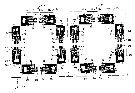
production process described later. Fig. 1 is a plan view wherein an N-type
magnetic sensor 10 and an S-type magnetic sensor 50 are placed side by
side. The N-type magnetic sensor 10 and the S-type magnetic sensor 50
have substantially the same shape and same configuration except that a
direction of fixed magnetization in a pinned layer shown by black-solid
arrows in Fig. 1 and a direction of magnetization in an initial state in a
free
layer shown by outline arrows in Fig. 1 are different from each other.
Accordingly, the following explanation is mainly focused on the N-type
magnetic sensor 10.
The magnetic sensor 10 comprises, as shown in Fig. 1, a single chip
(a single substrate or a monolithic chip) 10a made of a quartz glass, which
has a rectangular shape (almost square shape) viewed in a plane having
sides along an X-axis direction and Y-axis direction perpendicular to each
other, and has a little thickness in a Z-axis direction perpendicular to the
X-axis and Y-axis, plural insulating layers 10b (wiring layers are included in
this insulating layers) laminated on the substrate 10a shown in Fig. 3, a
total
of eight GMR elements 11 to 14, 21 to 24 formed on the uppermost layer
10b1 of the Insulating layers 10b and a total of eight initializing coils
(coils
for initializing) 31 to 34 and 41 to 44.
The first X-axls GMR element 11 is formed at a portion a little
downward from the almost central part in the Y-axis direction of the chip 10a
and in the vicinity of an end portion of the X-axis negative direction. The
18
CA 02445896 2003-10-21
direction of pinned magnetization of the pinned layer of the GMR element 11
is in the X-axis negative direction as shown by a black-solid arrow in Fig. 1.
The second X-axis GMR element 12 is formed at a portion a little upward
from the almost central part in the Y-axis direction of the chip i Oa and in
the
vicinity of the end portion of the X-axis negative direction. The direction of
pinned magnetization of the pinned layer of the GMR element 12 is in the
X-axis negative direction shown by a black-solid arrow in Fig. 1. The third
X-axis GMR element 13 is formed at a portion a little upward from the
almost central part in the Y-axis direction of the chip 10a and in the
vicinity
of an end portion of the X-axis positive direction. The direction of pinned
magnetization of the pinned layer of the GMR element 13 is in the X-axis
positive direction as shown by a black-solid arrow in Fig. 1. The fourth
X-axis GMR element 14 is formed at a portion a little downward from the
almost central part in the Y-axis direction of the chip 10a and in the
vicinity
of the end portion of the X-axis positive direction. The direction of pinned
magnetization of the pinned layer of the GMR element 14 is in the X-axis
positive direction shown by a black-solid arrow in Fig. 1.
The first Y-axis GMR element 21 is formed at a portion a little
leftward from the almost central part in the X-axis direction of the chip 10a
and in the vicinity of an end portion of the Y-axis positive direction. The
direction of pinned magnetization of the pinned layer of the GMR element 21
is in the Y-axis positive direction as shown by a black-solid arrow in Fig. 1.
The second Y-axis GMR element 22 is formed at a portion a little rightward
from the almost central part in the X-axis direction of the chip 10a and in
the
vicinity of the end portion of the Y-axis positive direction. The direction of
pinned magnetization of the pinned layer of the GMR element 22 is in the
19
CA 02445896 2003-10-21
Y-axis positive direction shown by a black-solid arrow in Fig. 1. The third
Y-axis GMR element 23 is formed at a portion a little rightward from the
almost central part in the X-axis direction of the chip 10a and in the
vicinity
of an end portion of the Y-axis negative direction. The direction of pinned
magnetization of the pinned layer of the GMR element 23 is in the Y-axis
negative direction as shown by a black-solid arrow In Fig. 1. The fourth
Y-axis GMR element 24 is formed at a portion a little leftward from the
almost central part in the X-axis direction of the chip 10a and in the
vicinity
of the end portion of the Y-axis negative direction. The direction of pinned
magnetization of the pinned layer of the GMR element 24 is in the Y-axis
negative direction shown by a black-solid arrow in Fig. 1.
Each of the GMR elements 11 to 14 and 21 to 24 has substantially
the same structure except for the position on the chip 10a. Therefore, the
first X-axis GMR element 11 is taken as a representative example
hereinbelow for explaining the structure thereof.
The first X-axis GMR element 11 comprises, as shown in Fig. 2 that
is a plan view and Fig. 3 that Is a schematic sectional view of the first X-
axis
GMR element 11 cut by a plane along a line of 1- 1 in Fig. 2, a plurality of
narrow zonal portions 11 a..... 11 a made of a spin valve film SV and having
a longitudinal direction in the Y-axis direction and bias magnet films (hard
ferromagnetic thin film layer and become a permanent magnet film by
magnetization) 11 b ..... 11 b that are made of hard ferromagnetic materials,
-having high coercive force and high squareness ratio, such as CoCrPt.
Each of the narrow zonal portions 11 a ..... 11 a extends in the X-axis
direction on the upper surface of each of the bias magnet films 11 b ..... 11
b,
and joins to the adjacent narrow zonal portion 11a to thereby form a
CA 02445896 2003-10-21
so-called "zig-zag shape" as well as to thereby magnetically join to each of
the bias magnet films 11 b ..... 11 b at the upper surface of each of the bias
magnet films 11 b ..... 11 b.
As shown in Fig. 4 that illustrates the film structure, the spin valve
film SV of the first X-axis GMR element 11 includes a free layer F, a
conductive spacer layer S made of Cu having a thickness of 2.4 nm (24A), a
fixed layer (pin (ayer) P and a capping layer C made of titanium (Ti) or
tantalum (Ta) having a thickness of 2.5 nm (25A), which are laminated in
this order on the chip 1Oa serving as a substrate.
The free layer F is a layer whose magnetization direction varies in
accordance with the direction of the external magnetic field, and comprises
a CoZrNb amorphous magnetic layer 11-1 formed directly on the substrate
10a and having a film thickness of 8 nm (80A), a NiFe magnetic layer 11-2
formed on the CoZrNb amorphous magnetic layer 11-1 and having a film
thickness of 3.3 nm (33A), and a CoFe layer 11-3 formed on the NiFe
magnetic layer 11-2 and having a film thickness of approximately 1 to 3 nm
(10 to 30A). The CoZrNb amorphous magnetic layer 11-1 and NiFe
magnetic layer 11-2 constitute a soft ferromagnetic material thin film layer.
The CoFe layer 11-3 prevents Ni of the NiFe magnetic layer 11-2 and Cu
11-4 of the spacer layer S from diffusing.
The fixed layer (pin layer) P is made by superposing a CoFe
magnetic layer 11-5 having a film thickness of 2.2 nm (22A), and an
antiferromagnetic film 11-6 which is formed of a PtMn alloy including 45 to
55 mol9'o of Pt and has a film thickness of 24 nm (240A). The CoFe
magnetic layer 11-5 is In an exchange coupling manner to the magnetized
antiferromagnetic film 11-6. Thus, the direction of magnetization
21
CA 02445896 2003-10-21
(magnetizing vector) of the CoFe magnetic layer 11-5 is pinned (fixed) in the
X-axis negative direction as described above.
The bias magnet films 11 b ..... 11 b gives a bias magnetic fieid to the
free layer F in the Y-axis negative direction (the direction shown by the
outline arrow in Figs. 1 and 2) that Is the longitudinal direction of the free
layer F in order to maintain uniaxial anisotropy of the free layer F.
The first X-axis GMR element 11 thus configured presents a
resistance value, which changes in almost proportion to the external
magnetic field that changes along the X-axis within a range of -Hc to +Hc,
as indicated by the solid line of Fig. 5, and presents an almost constant
resistance value to the external magnetic field that changes along the Y-axis,
as indicated by the broken line of Fig. 5.
Subsequently, the Initializing coils 31 to 34 and 41 to 44 are
explained. The initializing coils 31 to 34 and 41 to 44 are buried in the
lower insulating layer 10b2 under the uppermost layer 10b1 of the insulating
layers. The initializing coils 31 to 34 and 41 to 44 are positioned
approximately immediately below each of the GMR elements 11 to 14 and
21 to 24, respectively. Each of the initiaiizing coils 31 to 34 and 41 to 44
has the same shape to one another, and its relative positionaf relationship to
the corresponding GMR element immediately above each coil is the same to
one another. Each of the initializing coils 31 to 34 and 41 to 44 applies the
initializing magnetic field in the direction shown by the outline arrow in
Fig. 1
to each corresponding GMR element.
The following explanation is made by taking the initializing coil 31 as
a representative example. This initiaiizing coil 31 is wound so as to have
an approximately rectangular outer shape viewed in a plane, and comprises
22
CA 02445896 2003-10-21
plural initializing magnetic field generating sections 31 a ..... 31 a
extending
linearly in the direction (X-axis direction) perpendicular to the longitudinal
direction of the narrow zonal portions 11 a of the first X-axis GMR element
11 at a region immediately below the first X-axis GMR element 11 viewed in
a plane. Further, one end 31b and the other end 31c of the initializing coil
31 are connected to a positive polarity and negative polarity of a constant
voltage source respectively. When a predetermined condition is
established, predetermined current Is made to flow through the initializing
coil 31, thereby applying the initializing magnetic field in the Y-axis
negative
direction to the narrow zonal portion 11 a of the first X-axis GMR element 11
as shown by the outline arrow in Fig. 1.
Subsequently explained are an X-axis magnetic sensor (a magnetic
sensor with a magnetic field detecting direction which is the X-axis
direction)
and a Y-axis magnetic sensor (a magnetic sensor with a magnetic field
detecting direction which is the Y-axis direction) composed respectively of
the GMR elements 11 to 14 and 21 to 24. As shown by an equivalent
circuit in Fig. 6A, the X-axis magnetic sensor is formed such that the first
to
fourth X-a)is GMR elements 11 to 14 are full-bridge-connected via a
conductor not shown in Fig. 1. In Fig. 6A, each graph shown at the
position adjacent to each of the first to fourth GMR elements 11 to 14
indicates a characteristic (change in the resistance value R with respect to
the external magnetic field) of the GMR element adjacent to each graph.
This is also true in Figs. 7 to 9. Symbols Hx and Hy in these graphs
respectively indicate the external magnetic field whose magnitude varies
along the X-axis and Y-axis.
In this configuration, a connection point between the first X-axis
23
CA 02445896 2003-10-21
GMR element 11 and the fourth X-axis GMR element 14 and a connection
point between the second X-axis GMR element 12 and the third X-axis GMR
element 13 are respectivety connected to the positive polarity and the
negative polarity (ground) of the constant voltage source, whereby a
potential of +V (5 (V) in this embodiment) and a potential -V (0 (V) in this
embodiment) are respectively applied thereto. Then, a difference in
potential Vox between a connection point of the first X-axis GMR element 11
and the third X-axis GMR element 13 and a connection point of the fourth
X-axis GMR element 14 and the second X-axis GMR element 12 are taken
out as a sensor output. As a result, the X-axis magnetic sensor outputs, as
shown in Fig. 6B, an output voltage Vo, that varies in approximately
proportion to the external magnetic field Hx that changes along the X-axis.
As shown by an equivalent circuit in Fig. 7A, the Y-axis magnetic
sensor is formed such that the first to fourth Y-axis GMR elements 21 to 24
are full-bridge-connected via a conductor not shown In Fig. 1. A
connection point between the first Y-axis GMR element 21 and the fourth
Y-axis GMR element 24 and a connection point between the second Y-axis
GMR element 22 and the third Y-axis GMR element 23 are respectively
connected to the positive polarity and the negative polarity (ground) of the
constant voltage source, whereby a potential of +V (5 (V) in this
embodiment) and a potential of -V (0 (V) in this embodiment) are
respectively applied thereto. Then, a difference in potential Voy between a
connection point of the first Y-axis GMR element 21 and the third Y-axis
GMR element 23 and a connection point of the fourth Y-axis GMR element
24 and the second Y-axis GMR element 22 are taken out as a sensor output.
As a result, the Y-axis magnetic sensor outputs, as shown in Fig. 7B, an
24
CA 02445896 2003-10-21
output voltage VoY that varies in approximately proportion to the external
magnetic field Hy that changes along the Y-axis. The above description is
about the configuration of the N-type magnetic sensor 10.
On the other hand, the S-type magnetic sensor 50 includes GMR
elements 51 to 54 and 61 to 64 and initializing coils 71 to 74 and 81 to 84 as
shown in Fig. 1. The S-type magnetic sensor 50 has the substantially
same structure as that of the magnetic sensor 10 and includes the X-axis
magnetic sensor and Y-axis magnetic sensor.
Specifically, as shown by an equivalent circuit in Fig. 8A, the X-axis
magnetic sensor is formed such that the first to fourth X-axis GMR elements
51 to 54 are full-bridge-connected via a conductor not shown in Fig. 1. In
this configuration, a connection point between the first X-axis GMR element
51 and the fourth X-axis GMR element 54 and a connection point between
the second X-axis GMR element 52 and the third X-axis GMR element 53
are respectively connected to the positive polarity and the negative polarity
(ground) of the constant voltage source, whereby a potential of +V (5 (V) in
this embodiment) and a potential of -V (0 (V) in this embodiment) are
respectively applied thereto. Then, a difference in potential VoX between a
connection point of the first X-axis GMR element 51 and the third X-axis
GMR element 53 and a connection point of the fourth X-axis GMR element
54 and the second X-axis GMR element 52 are taken out as a sensor output.
As a result, the X-axis magnetic sensor outputs, as shown In Fig. 8B, an
output voltage Vox that varies in approximately proportion to the external
magnetic field Hx that changes along the X-axis.
Further, as shown by an equivalent circuit in Fig. 9A, the Y-axis
magnetic sensor of the magnetic sensor 50 is formed such that the first to
CA 02445896 2003-10-21
fourth Y-axis GMR elements 61 to 64 are full-bridge-connected via a
conductor not shown in Fig. 1. A connection point between the first Y-axis
GMR element 61 and the fourth Y-axis GMR element 64 and a connection
point between the second Y-axis GMR element 62 and the third Y-axis GMR
element 63 are respectively connected to the positive polarity and the
negative polarity (ground) of the constant voltage source, whereby a
potential of +V (5 (V) in this embodiment) and a potential -V (0 (V) in this
embodiment) are respectively applied thereto. Then, a difference in
potential Voy between a connection point of the first Y-axis GMR element 61
and the third Y-axis GMR element 63 and a connection point of the fourth
Y-axis GMR element 64 and the second Y-axis GMR element 62 are taken
out as a sensor output. As a result, the Y-axis magnetic sensor outputs, as
shown in Fig. 9i3, an output voltage Voythat varies in approximately
proportion to the external magnetic field Hy that changes along the Y-axis.
Subsequently explained is a process for manufacturing the magnetic
sensors 10 and 50 thus configured as described above. Firstly, each
insulating layer 10b is laminated on a rectangular quartz glass (wafer) 10a1,
that becomes the substrates 10a and 50a later, with the formation of a
predetermined wiring or LSI, followed by forming the initializing coils 31 to
34, 41 to 44, 71 to 74 and 81 to 84 in the insulating layer 10b2, and then,
the uppermost insulating layer 10b1 is formed (see Figs. 1 to 3).
Then, plural films M composing the GMR elements 11 to 14, 21 to
24, 51 to 54 and 61 to 64 are formed like an island. Specifically, said bias
films 11 b are formed and said films M which will become GMR elements 11
to 14, 21 to 24, 51 to 54 and 61 to 64 are formed on the bias film 11 b. This
film formation is performed by using a ultra-high vacuum device in a manner
26
CA 02445896 2003-10-21
of continuous laminating with a precise thickness. The fiims M are
patterned and thereby plural island-like portions which will become the GMR
elements are formed. These films M are formed to be arranged at each
position of the GMR elements 11 to 14, 21 to 24, 51 to 54 and 61 to 64
shown in Fig. I when the quarts glass 10a1 is cut along the broken line in
Fig. 10 by a subsequent cutting process to thereby be divided into the
Individual magnetic sensor 10 and 50 shown in Fig. 1.
Subsequently, as shown in Fig. 11 that Is a plan view, a rectangular
metal plate 91 is prepared that is provided only with plural square
through-holes arranged in a tetragonal lattice (i.e., square through-holes
each having sides parallel to the X-axis and Y-axis are arranged along the
X-axis and Y-axis so as to be spaced at equal intervais). Each of
permanent bar magnets 92 ..... 92 with a shape of a rectangular
parallelepiped having a square section approximately equal to each
through-hole is inserted into each through-hole such that the edge face
having a magnetic pole of the permanent bar magnet 92 ..... 92 formed
thereon becomes parallel to the metal plate 91. At this time, the
permanent bar magnets 92 ..... 92 are arranged such that the polarity of the
magnetic pole is different from the adjacent polarity by the shortest route in
a plane including each edge face of the permanent bar magnets 92 ..... 92.
It is to be noted that each of the used permanent bar magnets 92 ..... 92 has
magnetic charge whose magnitude is approximately equal to one another.
Then, as shown in Fig. 12 that represents a section along X-Z plane,
a plate 92 is prepared that is made of a transparent quartz glass having a
thickness of about 0.5 mm and having a rectangular shape approximately
equal to the metal plate 91. Thereafter, the upper surface (the surface
27
CA 02445896 2003-10-21
opposite to the edge face on which the magnetic pole Is formed) of the
permanent bar magnets 92 ..... 92 and the bottom surface of the plate 93
are bonded by an adhesive, and then, the metal plate 91 is removed from
below. At this stage, a magnet array MA is formed by the permanent bar
magnets 92 ..... 92 and the plate 93, wherein plural permanent magnets,
each having an approximately rectangular parallelepiped shape in which the
sectional shape perpendicular to one central axis of the rectangular
parallelepiped is approximately square, are arranged such that the center of
gravity of the edge face having approximately square shape Is matched with
a lattice point of the tetragonal lattice, and the polarity of the magnetic
pole
of each permanent magnet thus arranged is different from the polarity of the
magnetÃc pole of the adjacent other permanent magnet spaced by the
shortest route.
Fig. 13 is a perspective view showing a state wherein only four
permanent bar magnets 92 ..... 92 are taken out. As apparent from this
figure, there are magnetic fields formed on the edge face (the edge face on
which the magnetic pole is formed) of the permanent bar magnet 92 .... 92,
the magnetic fields from one N-pole directing to the S-poles adjacent to this
N-pole by the shortest route and each having a different direction at an
angle of 90 degrees. In this embodiment, this magnetic field is used as a
magnetic field for magnetizing each bias magnet film 11 b to 14b, 21 b to 24b,
51 b to 54b and 61 b to 64b of each GMR element 11 to 14, 21 to 24, 51 to
54 and 61 to 64 and as a magnetic field for fixing the direction of
magnetization in each fixed layer P (pinned layer in the fixed layer P).
Specificaily, as shown in Fig. 14, the quartz glass 10a1 on which the
film M which will become the GMR element is formed is firstly arranged such
28
CA 02445896 2003-10-21
that the face having the film M which will become the GMR element formed
thereon comes in contact with the upper surface of the plate 93, and then,
the plate 93 and the quartz glass 10a1 are fixed to each other by a cramp C.
At this time, as shown in Fig. 15 that is a plan view for enlarging the
section
that becomes later the magnetic sensors 10 and 50 by paying attention to
the section corresponding to two of the magnetic sensors 10 and 50, the
quartz glass 10a1 and the magnet array MA are relatively arranged such
that each cross-point CP of the cutting plane line CL of the quartz glass
10a1 that becomes each side of the magnetic sensors 10 and 50 is matched
with the respective center of gravity of the permanent bar magnets 92 .....
92. Accordingly, as shown by arrows in Fig. 15, a magnetic field is applied
to each film M which will become the GMR element in the longitudinal
direction of the narrow zonal portion of each film M in the state wherein the
quartz glass 10a1 is placed on the upper surface of the plate 93.
The present embodiment utilizes this magnetic field for magnetizing
the bias magnet films 11 b to 14b, 21 b to 24b, 51 b to 54b and 61 b to 64b as
well as for matching the direction of magnetization In each magnetic domain
in the free layer F with the direction in the initial state. That is ,
magnetization in each magnetic domain in the free layer F is initialized.
Subsequently, the relative relationship between the quartz glass
10a1 having the film M which will become the GMR element formed thereon
and the magnet array MA (plate 93) is changed as shown in a plan view of
Fig. 16, whereby the surface on which the film M which will become the
GMR element is formed is arranged to be brought Into contact with the
upper surface of the plate 93. At this time, the quartz glass 10a1 and the
magnet array MA are relatively arranged such that each cross-point of the
29
CA 02445896 2003-10-21
cutting plane line CL of the quartz glass 10a1 that becomes each side of the
magnetic sensors 10 and 50 is matched with the respective center of gravity
of the four adjacent permanent bar magnets 92 ..... 92. Accordingly, as
shown by arrows in Fig. 16, a magnetic field is applied to each film M which
will become the GMR element in the direction perpendicular to the
longitudinal direction of the narrow zonal portion of each film M in the state
wherein the quartz glass 10a1 is placed on the upper surface of the plate
93.
The present embodiment utilizes this magnetic field for performing a
heat treatment (annealing for ordering) to fix the direction of magnetization
in the fixed layer P (pinned layer of the fixed layer P). Specifically, the
plate 93 and the quartz glass 10a1 are fixed to each other by the cramp C
with the state shown in Fig. 16, then, the resultant is heated in a vacuum to
250 to 280 "C and left for about four hours in this state.
Thereafter, the quartz glass 10a1 is removed to form a wiring or the
like for connecting each film M, and finally, the quartz glass 10a1 is cut
along the broken line (or the cutting line CL) shown in Fig. 10 etc.. As
described above, a great number of magnetic sensors 10 and 50 shown in
Fig. 1 are simultaneously produced.
As described above, a magnetic sensor according to the
embodiment of the present Invention has bias magnet films 11 b ..... 11 b
provided at both ends of the free layer F in the longitudinal direction for
producing in the free layer a bias magnetic field In a predetermined direction
(in the longitudinal direction of the free layer), whereby the direction of
magnetization in each magnetic domain in the free layer can stably be
maintained in the predetermined direction when an external magnetic field is
CA 02445896 2003-10-21
not present.
Further, the initializing coils 31 to 34 and 41 to 44 are energized
under a predetermined condition to thereby generate an initializing magnetic
field for returning the direction of magnetization in each magnetic domain in
the free layer to the direction (i.e., the longitudinal direction of the free
layer)
same as the direction of the bias magnetic field by the bias magnet films,
whereby the direction of magnetization in each magnetic domain In the free
layer can assuredly be returned to the initial state even if the direction of
magnetization is disturbed by applying a strong magnetic field to the free
layer. As a result, a hysteresis that occurs when the external magnetic
field is in the vicinity of "0" with respect to the change of the external
magnetic field can be maintained small of the magnetic sensors 10 and 50.
Thus, the magnetic sensor is capable of detecting a minute magnetic field
with high precision over a long period.
Further, according to the production process of the magnetic sensor
according to the embodiment of the present invention, there is prepared a
magnet array MA that is configured such that plural permanent magnets are
arranged at a lattice point of a tetragonal iattice and the polarity of the
magnetic pole of each permanent magnet is different from the polarity of the
other adjacent magnetic pole spaced by the shortest route. Therefore, the
direction of magnetization in each magnetic domain in the free layer Is
initialized and the bias magnet films are magnetized, and further, a pinning
is performed by pinning the direction of magnetization in the magnetic layer
that becomes a pinned layer. Accordingly, plural GMR elements having
different magnetic field detecting directions (perpendicular to each other)
can easily and efficiently be formed on a single chip, thereby being capable
31
CA 02445896 2003-10-21
of manufacturing with low cost a magnetic sensor of a single chip which is
capable of detecting at least respective magnetic fields whose magnitude Is
changed in the directions perpendicular to each other.
It should be noted that, In the above embodiment, the films M for
GMR films (films M which will be the GMR elements) are formed after the
bias films (films for magnets) are patterned, and the films M for GMR films
are annealed for ordering after the GMR films are patterned. However, the
annealing process for ordering can be performed before the films M for
GMR films are patterned. Further, the bias films can be formed after the
films M for GMR films are formed.
Next, another embodiment of a magnetic sensor (second
embodiment) in accordance with the present invention will be described.
This magnetic sensor is also classified into N-type shown in Fig. 21 which is
a plan view of the N-type sensor and S-type shown in Fig. 22 which is a plan
view of the S-type sensor. The N-type magnetic sensor 110 and the S-type
magnetic sensor 150 have substantially the same shape and same
configuration except that a direction of fixed magnetization in a pinned layer
shown by black-solid arrows In Figs. 21 and 22 and a direction of
magnetization in an initial state in a free layer shown by outline arrows in
Figs. 21 and 22 are different from each other. Note that, initializing coils
are omitted in Figs. 21 and 22.
The N-type magnetic sensor 110 has the same structure as the
N-type magnetic sensor 10 except the position of the GMR elements and
the initializing coils. The N-type magnetic sensor 110 comprises a single
chip 1 10a which Is the same as the single chip 10a, insulating layers which
is the same as the insulating layers 10b, a total of eight GMR elements 111
32
CA 02445896 2003-10-21
to 114, 121 to 124 formed on the uppermost layer of the insuiating layers
and a total of eight Initializing coils (coils for initializing). A relative
positional relationship between the GMR elements 111 to 114, 121 to 124
and the eight initializing coils is the same as that between the GMR
elements 11 to 14, 21 to 24 and the initializing coils 31 to 34, 41 to 44.
The GMR elements 111 to 114 form an X-axis magnetic sensor by being
full-bridge-connected similarly to the GMR elements 11 to 14. The GMR
elements 121 to 124 form an Y-axis magnetic sensor by being
fuil-bridge-connected similarly to the GMR eiements 21 to 24.
The first X-axis GMR element 111 is formed at an almost central
portion in the Y-axis direction of the chip 110a and in the vicinity of an end
portion of the X-axis negative direction. The second X-axis GMR element
112 is formed at an almost centrai portion in the Y-axis direction of the chip
11-aa and at a portion spaced by a predetermined short distance in the
X-axis positive direction from the first X-axis GMR element 111. The third
X-axis GMR element 113 is formed at an almost central portion in the Y-axis
direction of the chip 110a and in the vicinity of an end portion of the X-axls
positive direction. The fourth X-axis GMR element 114 is formed at an
almost central portion in the Y-axis direction of the chip 110a and at a
portion spaced by a predetermined short distance in the X-axis negative
direction from the third X-axis GMR element 113. An each of longitudinal
directions of the first to fourth X-axis GMR elements 111 to 114 is parallel
to
the Y-axis direction.
The first Y-axis GMR element 121 Is formed at an almost central
portion in the X-axis direction of the chip 110a and in the vicinity of an end
portion of the Y-axis positive direction. The second Y-axis GMR element
33
CA 02445896 2003-10-21
122 is formed at an almost central portion in the X-axis direction of the chip
110a and at a portion spaced by a predetermined short distance in the
Y-axis negative direction from the first Y-axis GMR element 121. The third
Y-axis GMR element 123 is formed at an almost central portion in the X-axis
direction of the chip 110a and in the vicinity of an end portion of the Y-axis
negative direction. The fourth Y-axis GMR element 124 is formed at an
almost central portion in the X-axis direction of the chip 110a and at a
portion spaced by a predetermined short distance in the Y-axis positive
direction from the third Y-axis GMR element 123. An each of iongitudinai
directions of the first to fourth Y-axis GMR elements 121 to 124 is parallel
to
the X-axis direction.
The S-type magnetic sensor 150 has the same structure as the
S-type magnetic sensor 50 except the position of the GMR elements and the
initiaiizing coils. The magnetic sensor 150 comprises a single chip 150a
which is the same as the single chip 50a, insulating layers which is the
same as the insulating layers 10b, a total of eight GMR elements 151 to 154,
161 to 164 formed on the uppermost layer of the insulating layers and a total
of eight initializing coils (coils for initializing). A relative positional
relationship between the GMR elements 151 to 154, 161 to 164 and the
eight initializing coils is the same as that between the GMR elements 51 to
54, 61 to 64 and the initializing coils 71 to 74, 81 to 84. The GMR
elements 151 to 154 form an X-axis magnetic sensor by being
full-bridge-connected similarly to the GMR elements 51 to 54. The GMR
elements 161 to 164 form an Y-axis magnetic sensor by being
full-bridge-connected similarly to the GMR elements 61 to 64.
A positional relationship between the first to fourth X-axis GMR
34
CA 02445896 2003-10-21
elements 151 to 154 and the substrate 150a is the same as that between
the first to fourth X-axis GMR elements 111 to 114 and the substrate 110a.
An each of longitudinal directions of the first to fourth GMR elements 151 to
154 is parallel to the Y-axis, direction. A positional relationship between
the
first to fourth Y-axis GMR elements 161 to 164 and the substrate 150a is the
same as that between the first to fourth Y-axis GMR elements 121 to 124
and the substrate 110a. An each of longitudinal directions of the first to
fourth GMR elements 161 to 164 is parallel to the X-axis direction.
Subsequently explained is a process for manufacturing the magnetic
sensors 110 and 150 thus configured as described above. In this process,
the magnet array MA described above and a magnet array MB which is
different from the magnet array MA are used.
Firstly, the magnet array MA is prepared by the process mentioned
above and the magnet array MB is prepared by the following process below.
Prior to the process to make the magnet array MB, each of parts that
constitute magnet array MB is explained. The magnet array MB comprises
a yoke (yoke plate) 200, a substrate for the array 210 and plural permanent
magnets (permanent bar magnets) 230.
The yoke 200 is shown in Figs. 23, 24 and 25. Fig. 23 is a
fragmentary plan view of the yoke 200, Fig. 24 is an enlarged plan view of
Fig. 23 and Fig. 25 is a sectional view of the yoke shown in Fig. 24 cut by a
plane along a line 2 - 2 in Fig. 24. This yoke 200 is a thin plate formed of
magnetic material which has larger permeability than air (e.g., 42 alloy ===
Fe-42Ni alloy and the like). Preferably, yoke 200 can be formed of high
saturation - high permeability material such as permalloy or silicon steel
(silicon sheet). The planar shape of the yoke Is rectangle. The plate
CA 02445896 2003-10-21
thickness of the yoke 200 Is 0.15 mm in this example. The yoke 200 has
plural thorough holes 201. The through hole 201 has an approximately
square shape viewed in a plane. The plural through holes 201 are
arranged in a tetragonai lattice. Specifically, the through holes 201 are
disposed such that each center of gravity of the through holes 201 is
matched with a lattice point SP of the tetragonal lattice shown In Fig. 24.
As viewed in a plane, a certain side of sides forming the through hole 201 is
parallel to a certain side of sides forming the adjacent through hole 201. In
other words, a certain side of sides forming the through hole 201 and a
certain side of sides forming other through hoie 201 located on the same
row (or column) of the tetragonal lattice are on (in) a same straight line.
Each of the through holes 201, as shown in, Fig. 26 showing a planar
shape of the through hole 201, has a shape composed of a square portion
201 a and margin portions (circle arc portions or R portions) 201 b viewed in
a piane. A shape of the square portion 201a is a square. The margin
portion 201 b swells outwardly from the square at each of corners of the
square portion 201 a. Specifically, an outer shape (outline) of the margin
portion 201 b Is a circle arc whose center PR is on a diagonal line CR of the
square portion 201 a.
Through openings 202 serving as air gaps are formed between the
through hole 201 and the other adjacent through hole 201 spaced by the
shortest route from the former through hole 201( i.e., between through holes
201, 201 that are adjacent each other with a shortest distance). A shape of
the through opening 202 is approximately a rectangle in viewed in a plane.
A longer side of the through opening 202 is parallel to a side of the square
portion 201 b of the through hole 201 next to the same through opening 202.
36
CA 02445896 2003-10-21
Length of the longer side of the through opening 202 Is approximately the
same as or is slightly shorter than length of the side of the square portion
201 a. Length of the shorter side of the through opening 202 is longer than
length of the longer side (side in the longitudinal direction) of each of the
films M which will become GMR elements 111 to 114, 121 to 124, 151 to
154 and 161 to 164.
The yoke 200 has openings (openings for controlling magnetic flux)
203. The opening 203, viewed in a plane, Is formed at a region
surrounding a center of gravity SQ of a square drawn by lines connecting
the lattice points of the tetragonal lattice. One of the openings 203 has a
shape of a circle whose center is on the center of gravity SQ viewed in a
plane.
The substrate for the array 210, shown in Figs 27 and 28, is a
substrate made by processing a thin plate 210a, shown in Fig. 29, formed of
magnetic materlal (e.g., permalloy). The substrate for the array 210 has
almost the same shape as the yoke 200 viewed in a plane. The substrate
for the array 210 includes plural concavities (ditches) 210b. Plural
concavities 210b are formed at the same positions (same locations) as the
through holes 201 of the yoke 200. A shape of the concavity 210b is
almost the same as the shape of the square portion 201 a of the through
hole 201.
The permanent bar magnets 230 has a shape of a rectangular
parallelepiped shape (see. Fig 31.). The permanent bar magnet 230 has a
sectional shape, perpendicular to one relatively longer central axis of the
rectangular parallelepiped, which is an approximately square shape
approximately same as the shape of the through hole 201 (and the
37
CA 02445896 2003-10-21
concavity 210b). Poles of the permanent bar magnet 230 are formed at
both edge faces each of which has the square shape. Magnitude of each
of magnetic charges of the plural permanent bar magnets 230 is
approximately equal to one another.
Subsequently explained is a process for manufacturing the magnet
array MB. Firstly, a thin plate which will become the yoke 200 is prepared.
The through holes 201, the through openings 202 and the openings 203 are
formed in the thin plate by etching. Next, the concavities 210b are formed
on the thin plate 210a which will become the substrate for the array 210 by
etching (by half-etching).
Next, square column-like spacers (bar) 220 are disposed on the
substrate for the array 210, as shown In Fig. 30 which is a perspective view
and in Fig. 31 which is a sectional view. The spacers 220 are placed
between one row constituted by the plural concavities 210b and the other
row, constituted by the plural concavities 210b, which is next to and is
parallel to the former row. When the spacers 220 are arranged in this
manner, length of the spacer 220 along the Z-axis direction is shorter than
length between both edge faces having magnetic poles of the permanent
bar magnet 230. Note that the margin portions 201 b are omitted In Fig. 30.
Subsequently, the yoke 200 is placed (disposed or arranged) on the
spacers 220. At this time, the yoke 200 is arranged In such a manner that
the through holes 201 (the square portions 201 a) of the yoke 200 and the
concavities 210b of the substrate for the array 210 coincide In a plan view.
In other words, in a state where the yoke 200 is disposed on the spacers
220, each of the concavities 210b coincides with each one of the through
holes 201 in a Z-axis direction. Note that a mark for determining position
38
CA 02445896 2003-10-21
of them (i.e., an alignment mark) may be formed on the yoke 200 and the
substrate for the array 210.
Next, each of the plural permanent bar magnets 230 is inserted Into
each of the plural through holes 201. At the time of the insertion of the
permanent bar magnets 230, one of the edge faces having magnetic poles
of the permanent bar magnets 230 is made to be in abutment (contact) with
each of upper surfaces of the concavities 210b of the substrate for the array
210. As a result, the other edge faces having magnetic poles of the
permanent bar magnets 230 (this face is also simply referred to as "upper
surface of the magnet 230 hereinafter) is placed (disposed) in a same
plane (on a single plane). Also, at this time, in the plane where the upper
surfaces of the magnet 230 is disposed, a polarity of a magnet pole of each
permanent magnet 230 is different from (opposite to) a polarity of the other
adjacent magnet pole spaced by the shortest route (i.e., shortest distance).
Accordingly, the permanent bar magnet 230 is arranged as shown in Fig 23.
In this stage, a movement of the permanent bar magnets 230 in a side
direction (in a transverse direction) is prohibited because the magnets 230
are inserted into both the through holes 201 of the yoke 200 and the
concavities 210b.
Next, the yoke 200 is lifted upwardly (in the Z-axis positive direction)
by utilizing the openings 203 of the yoke 200. More specifically, two of the
openings 203 are grasped with tweezers and the yoke 200 is lifted by the
tweezers. This operation Is repeated for the other openings 203 and the
whole yoke is gradually lifted upward. At this time, as shown in Fig. 33,
height of the yoke 200 (distance between the yoke 200 and the substrate for
the array 210) is adjusted in such a manner that the plane formed by the
39
CA 02445896 2003-10-21
upper surfaces of the permanent bar magnets 230 (i.e., all the other edge
faces having magnetic poles of the permanent bar magnets 230) is placed
between an upper surface 200up of the yoke 200 and a lower surface 200dn
of the yoke 200. In other words, the yoke 200 is lifted upwardly such that
the upper surface of the permanent bar magnet 230 is made to be within
plate thickness of the yoke 200. It should be noted that a plane formed by
the upper surface 200up of the yoke 200 coincides with a plane formed by
the upper surfaces of the permanent bar magnets 230. Then, the spacers
are taken out and the yoke 200 Is fixed to the substrate for the array 210.
The magnet array MB is thus completed.
Fig. 34 is a perspective view showing a state wherein only four
permanent bar magnets 230 ..... 230 are taken out. As is apparent from
this figure, there are provided magnetic fields from one N-pole directing to
the S-poles adjacent to this N-pole by the shortest route and each having a
different direction at an angle of 90 degrees, above the upper surfaces
(edge faces having the pole) of the permanent bar magnets 230 ..... 230.
In this embodiment, this magnetic field given by the magnet array MB Is
used as a magnetic field for magnetizing each bias magnet film of each
GMR element 111 to 114, 121 to 124, 151 to 154 and 161 to 164.
This magnet array MB has through openings 202 serving as air gaps
formed between two of (upper surfaces of) the permanent bar magnets 230
that are spaced by the shortest route and next to each other. With this
cinfiguration, as shown in Fig.35, magnetic flux concentrates both in the
through openings 202 and in a space close to the through openings 202.
In other words, the magnet array MB can provide a narrow space local
region with a magnetic field whose magnitude is great and whose direction
CA 02445896 2003-10-21
is stably constant.
Figs. 36 and 37 show states of magnetic flux generated by the
magnet array MB and the magnet array MA by arrows, respectively. As
understood by comparing one of the figures with the other figure, the
magnet array MB has not only above mentioned through openings 202 but
also openings 203, and therefore, it can make the magnetic field formed
between both the permanent bar magnets that are next to each other and
are spaced by the shortest route more linear and can provide locally the
magnetic field which is more stable and whose magnitude is greater than
the magnetic field provided by the magnet array MA.
With these steps mentioned above, the magnet array MA and the
magnet array MB are prepared. Therefore, the concrete process (method)
for manufacturing (producing) the magnetic sensors 110 and 150 is
explained, hereinafter.
Firstly, a substrate (a quartz glass that will become a substrate
110a1 described later with reference to Fig. 39, a wafer) is prepared on
which films M, which will become the GMR elements 111 to 114, 121 to 124,
151 to 154, 161 to 164, are formed. This substrate is formed in a manner
similar to the substrate 10a1 shown in Fig. 10. These films M are arranged
in such a manner that, when this substrate is cut in the cutting process
which will be carried out later, individual magnetic sensors 110 and 150
shown in Figs. 21 and 22 are obtained.
Next, the above mentioned substrate on which films M which will
become the GMR elements are formed and the magnet array MA (the plate
93) are arranged as shown in Fig. 38, and relative positional relationship
between them is fixed. At this time, they are disposed in such a manner
41
CA 02445896 2003-10-21
that a surface on which the films M which will become the GMR elements
are formed is made to come in contact with (be in abutment with) an upper
surface of the plate 93 (see. Fig 14.). Further, the substrate and the
magnet array MA are relatively arranged in such a manner that each
cross-point CP of the cutting plane line CL of the substrate that becomes
each side of the magnetic sensors 110 and 150 Is matched with the
respective center of gravity of the four adjacent permanent bar magnets
92 ..... 92. As a result, a magnetic field is applied to each film M which
will
become the GMR element in the direction perpendicular to the longitudinal
direction of the narrow zonal portion of each film M in the state wherein the
substrate is placed on the upper surface of the magnet array MA, as shown
by arrows in Fig. 38.
This second embodiment utilizes this magnetic field for performing a
heat treatment to fix the direction of magnetization in the fixed layer P
(pinned layer of the fixed layer P). Specifically, the plate 93 and the
substrate are fixed to each other by the cramp C (see. Fig. 14) with the state
shown in Fig. 38, then, the resultant is heated in a vacuum to 250 to 280 'C
and left for about four hours in this state (i.e., the annealing for ordering
is
performed).
Next, as shown in Fig. 39, the substrate 110a1 on which the films M
which will become the GMR elements are formed is arranged in such a
manner that the plane on which the films M which will become the GMR
elements are formed comes in contact with (is in abutment with) the upper
surface 200up of the yoke 200 of the magnet array MB. At this time, as
shown in Fig 40 which is a fragmentary enlarged plan view, the substrate
and the magnet array MB are relatively arranged in such a manner that each
42
CA 02445896 2003-10-21
cross-point CP of the cutting plane (ine CL of the substrate 110a1 that
becomes each side of the magnetic sensors 110 and 150 is matched with
the respective center of gravity of the each permanent bar magnet 230 .....
230. At this time, the films M which will be the GMR elements is disposed
inside of the through openings 202 of the yoke 200, in viewed in a plane.
Accordingly, as shown by arrows in Fig. 40, a magnetic field is applied to
each film M which will become the GMR element in the longitudinal direction
of the narrow zonal portion of each film M in the state wherein the substrate
110a1 is placed on the upper surface 200up of the yoke 200,
This second embodiment utilizes this magnetic field for magnetizing
the bias magnet films as well as for matching the direction of magnetization
in each magnetic domain in the free layer F with the direction in the initial
state.
Thereafter, the substrate 110a1 Is removed to form a wiring or the
like for connecting each film M, and finally, the substrate 110a1 is cut along
the broken line shown in Figs. 38 and 40_ As described above, a great
number of monolithic (single chip) magnetic sensors 110 shown in Fig. 21
and monolithic (single chip) magnetic sensors 150 shown in Fig. 22 are
simultaneously produced.
As explained above, in the second embodiment, the strong magnetic
field is provided at local space by utilizing the magnet array MB, and the
magnetic field thus provided is used to magnetize the the bias magnet films
of the GMR elements. The magnet array MB comprises the yoke having
through openings 202 serving as air gaps. Therefore, the magnet array
MB can provide a space close to the through openings 202 with a magnetic
field whose magnitude is great and which is stably constant. Accordingly,
43
CA 02445896 2003-10-21
even if the magnetic materlal having a high coersive force is adopted to the
bias magnetic film, the bias magnetic film can be assuredly magnetized.
As a result, a high reliable magnetic sensor 110 and 150 can be provided in
which the direction of magnetization in the free layer is stably returned to
the
Initial-state direction even after the strong disturbance (e_g., a magnetic
field
whose magnitude is relatively large) is added to the magnetic sensor.
In addition, the yoke 200 has the openings 203 formed at regions
where the magnetic fields are unstable because of crossing (or collision) of
magnetic flux lines stemming from the poles. As a result, since the
direction of the magnetic flux lines become stable, the magnetic field in the
region in the neighborhood of the through opening 202 becomes more
stable. Further, the openings 203 are used to adjust the distance between
the substrate for the array 210 of the magnet array MB and the yoke 200
(i.e., the height of the yoke 200). Therefore, since it is possible to adjust
the height of the yoke easily and desirably, an optimum magnetic field can
be provided for a region where the bias magnetic film of the GMR element is
disposed to be magnetized.
Moreover, the through hole 201 of the yoke 200 of the magnet array
MB has the shape which is not a square shape but which includes the
margin portions 201 b swelling outwardly from the square at each of corners
of the square. Therefore, when forming the through hoie 201 by etching,
even if the corner of the through hole is not completely etched as designed,
the permanent bar magnet 230 can be assuredly inserted into the through
hole 201. It should be noted that this type of margin portion may preferably
be formed at corners of the concavities 210b.
The present invention is not limited to the above-mentioned
44
CA 02445896 2003-10-21
embodiment, but various modifications can be applied within the scope of
the present Invention. For example, as shown in Fig. 20 representing a
first X-axis GMR element 301 taking as a representative example, narrow
zonal portions 301 a may be separated at the upper portion of the bias
magnet films 301 b ..... 301 b disposed below both ends thereof. Further, an
initializing coil 302 may be a double spiral type coil wherein a spiral coil
302-1 having a center point P1 and a spiral coil 302-2 having a center point
P2 are connected to each other. In this case, the first X-axis GMR element
301 is arranged between the center point P1 and the center point P2,
resulting in that currents parallel to each other flow in the same direction
(in
a direction perpendicular to the longitudinal direction of the narrow zonal
portions 301 a) through each conductor section of the initializing coil 302
passing below the first X-axis GMR element 301, thereby generating the
initializing magnetic field. Moreover, the Initializing coil may be a
multi-layered coil or may be a toroidal coil. Further, a testing coil that
generates a testing magnetic field, in the direction perpendicular to the
initializing magnetic field generated by the initializing coil, for checking a
function of each GMR element may also be disposed in the Insulating layer
above or below (Z-axis direction) the initializing coil.
46