Note: Descriptions are shown in the official language in which they were submitted.
CA 02445971 2003-10-30
WO 02/088810 PCT/US02/13490
ALIGNMENT APERTURES IN AN OPTICALLY TRANSPARENT SUBSTRATE
Cross Reference to Related Applications
[0001] This application claims the benefits of U.S. Provisional Application
Numbers
60/287,762, and 60/289,355, filed May 1st, 2001, and May 8, 2001,
respectively.
Field of the Invention
[0002] The field of the invention relates to optoelectric data transmission
systems, and
alignment and interconnection of optical components.
Background of the Invention
[0003] In coupling optical waveguides or optical components together,
precision
alignment is important. When two optical components are placed together with
the-objective of
accurately transferring optical signals, the connection between the two
interfaces must~be within
a tight tolerance to achieve high coupling efficiency. A guiding mechanism is
typically used to
achieve the required tolerances in connecting two mating optical components.
This results in
improved optical coupling efficiency.
[0004] Solder is often used to mechanically and electrically connect parts.
During a
solder reflow process though, interlinked components may expand at different
rates if made of
differing materials. This differential expansion can induce unwanted stresses
on components,
further leading to cracking, misalignment, or detaching of components. These
unwanted results
could be exacerbated if alignment tolerances between interlinked components
are already near
their tolerance limit. Mechanical stresses may also need to be controlled
within the storage and
operating temperatures of the device, and not just during solder reflow
procedures.
[0005] As stresses are induced on optical components, it is important to
ensure that
optical alignment in maintained. In addition, optical alignment should be
maintained after solder
-1-
CA 02445971 2003-10-30
WO 02/088810 PCT/US02/13490
reflow when optical connectors are attached to the assembly and the optical
device is
functioning. Low placement tolerances are often needed between components to
achieve the
necessary optical alignment. However, these alignment tolerances can be
difficult to achieve
between optical components. In addition, lower placement tolerances can
increase
manufacturing costs.
[0006] The invention, described herein, provides an integral solution to the
problem of
differing expansion rates and low placement tolerance requirements in optical
components. The
invention serves to relieve induced stresses on components while maintaining
component
alignment. In turn, by relieving induced stresses on optical components, this
can further broaden
material selection to extend to those materials that are cheaper in price but
traditionally have
undesirable mechanical/optical properties.
Brief Description of the Drawings
[0007] FIG. 1 is an exploded view of an optical subassembly and optical
connector under
an illustrated embodiment of the invention;
[0008] FIG. 2 is a top view of the optical subassembly and optical connector
as shown in
FIG. 1.
[0009] FIG. 3 is another exploded view of the elements shown in FIG. 1;
[00010] FIG. 4 is a front view of the substrate and optical array.
[0010] FIG. 5 illustrates the effects of thermal expansion on an
optoelectronic component
[0011] FIG. 6 is another exploded view of the optical subassembly and optical
connector
upon alignment of an optical array to optical fibers.
Description of the Drawings and Preferred Embodiment
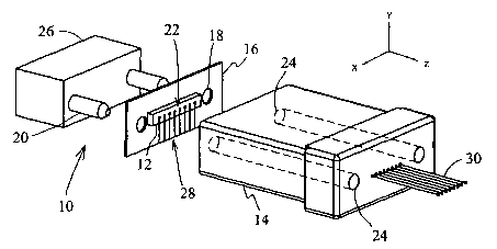
[0012] FIG. 1 shows an optical subassembly 10 and optical connector 14 in a
context of
use and generally in accordance with an illustrated embodiment of the
invention. Included
within the subassembly 10 may be an optical array 12 and an optically
transparent substrate 16 to
which the optical array 12 is attached. The optical array 12 may be
mechanically attached to the
substrate 16 by any conventional method such as stud bumps, adhesive, or
solder bumps (not
shown).
_2_
CA 02445971 2003-10-30
WO 02/088810 PCT/US02/13490
[0013] FIG. 2 illustrates a top view of the optical subassembly 10 and optical
connector
14 as first shown in FIG 1. As shown, the optical array 12 is attached to a
first surface 42 of the
substrate 16, such that optical signals 40 from the array 12 may pass directly
through the
transparent substrate. It will be understood that the optical array 12 can be
any suitable photonic
device or array of photonic devices including photo-transmitters, photo-
receivers, or a
combination thereof. A photo-transmitter can be any suitable device such as a
vertical cavity
surface emitting laser (VCSEL), light emitting diode (LED), or the like.
Furthermore, any
suitable photo-receiving device can be used, such as a photodiode, i.e., P-I-N
diode, PN diode, or
the like. Thus, the optical array 12 can be a broad range of photoactive
devices with transmitting
and receiving capabilities.
[0014] The optical array 12 may have a number of optical ports 22 (shown in
greater
detail in FIG. 4) for coupling optical signals 40 to/from a respective
photoactive device (not
shown). The optical ports 22 define the optically active surfaces of the
optical array 12. The
optical ports 22 provide a source or destination of optical transmission paths
40 to photonics
transmitters, receivers, or a combination of transmitters and receivers within
the optical array 12.
(The figures show the optical array 12 having eight optical ports 22, but the
array 12 may contain
any number of optical ports 22).
[0015] The optically transparent substrate 16 shown in FIGS. 1 and 2 may
contain a
plurality of electrical contacts and traces 28 for electrically connecting the
optical array 12 to a
signal processor (not shown). Electrical contacts may be defined on the
substrate 16 by
conventional photolithographic etching processing, or by any similar process.
The substrate 16
may comprise a glass-like structure having desirable optical and structural
properties. Materials
that have been found to display adequate properties include glass, plastic,
and sapphire. A form
of plastic commonly used in optics is Kapton ~. Although not optically
transparent, I~apton
has been found acceptable for use when a window is cut in the substrate for
optical signals to
pass through. The present invention could use any of the preceding materials
for a substrate, but
one of the preferred materials is glass.
[0016] Glass also has a thermal expansion coefficient that is much closer to
semiconductor devices (such as the optical array 12), as compared to the metal
substrates more
commonly used in photonics packaging. This reduces temperature-induced
misalignment
between packaged optical devices and externally coupled optical fibers 30.
Alignment features
-3-
CA 02445971 2003-10-30
WO 02/088810 PCT/US02/13490
18 may also be placed in or on the substrate with micron or submicron
accuracy, as described in
more detail below. This greatly simplifies the alignment of the optical ports
22 of the array 12
with optical fiber connectors 14 that may also have complementary alignment
structures 24
(described in further detail below).
[0017] The optically transparent substrate 16 and optical array 12 may then be
attached
to a guide pin holder 26, as shown in FIG. 2. Both the substrate 16 and array
12 may be attached
to the guide pin holder 26 by an appropriate adhesive. The adhesive should
allow for motion
between the two components while still maintaining attachment and correct
positioning. The
guide pin holder 26 may comprise a rigid material having appropriate
structural and thermal
properties. Materials showing suitable properties include but are not limited
steel and aluminum.
Shown in the figures are guide pins 20 that may protrude from a first surface
50 of the guide pin
holder 26. Furthermore, the guide pins 20 may comprise first and second guide
pins, 32 and 34
respectively. The guide pins 20 could be made of a stainless steel or other
material having
suitable structural and wear properties.
[0018] In addition to functioning as a holder for the guide pins 20, the guide
pin holder
26 may also function to remove heat from the optical array 12 and from
additional IC's (not
shown). Thus, the guide pin holder 26 should comprise a rigid material having
an adequate
thermal conductivity.
[0019] The guide pin holder 26 may also have a depression (not shown) on a
front
surface 50, such that the optical array 12 may fit into the space. Thus, the a
back surface 52, of
the optical array 12 and the first surface 42 of the substrate may
respectively be coincident with
the depression and first surface 50 of the pin holder 26.
[0020] Also shown on the optically transparent substrate 16 are alignment
apertures 18
which may properly align the optical ports 22 of the optical array 12 to a
plurality of optical
fibers 30 of the optical connector 14. In an illustrated embodiment of the
invention, the figures
show two alignment apertures 18 on either side of the optical array 12. Yet,
any number of
apertures 18 may be used. In addition, the figures illustrate circular
apertures 18, yet any shape
or size of apertures may be used for in the invention.
(0021] In a preferred embodiment of the present invention, the apertures 18
may be
disposed on opposing sides of the optical array 18, precisely positioned
relative to the optical
-4-
CA 02445971 2003-10-30
WO 02/088810 PCT/US02/13490
array 12. Specifically, the apertures may be disposed in the substrate at an
appropriate distance
from the optical ports 22 of the array 12.
[0022] Alignment apertures 18 may be formed using conventional techniques such
as
laser ablation, chemical etching, plasma etching, or a similar process. In a
preferred embodiment
of the present invention as shown in FIG. 3, a laser ablation technique with a
boring fixture 68
may be used. The boring fixture 68 may include a pattern recognition module 70
and lasers 72,
74. The pattern recognition module 70 may include soi~ware adapted to
recognize and position
itself over a line of targets.
[0023] Once recognition of the targets has occurred, the pattern recognition
module 70
functions to identify a transverse line passing through the line of targets as
well as a center point
of the line of targets. The pattern recognition module 70 then positions its
own transverse line
and center point with the identified transverse line and center point. The
lasers 72, 74 may be
precisely aligned along the transverse line of the pattern recognition module
70. The lasers 72,
74 are also positioned a precise distance on either side of the center point
of the pattern
recognition module 70.
[0024] The pattern recognition module 70 may be programmed to view the array
12
through the transparent substrate 16 and identify a set of alignment targets.
In a preferred
embodiment of the invention, the optical ports 22 may be used as alignment
targets for the
pattern recognition module 70 to identify. Once the pattern recognition module
70 has aligned
itself with the registration targets (and also the lasers 72, 74 on either
side of the targets as
shown), the boring fixture 68 activates the lasers 72, 74 to ablate the holes
18 in precise
alignment with the ports 22.
[0025] Included within the boring fixture 68 may be a precision lateral drive
mechanism
76. The precision lateral drive mechanism 76 may function to offset the
position of one of the
boring devices (e.g., 74) by a predetermined distance "a" along a center line
of the ports 22 on
either side of a nominal position. The nominal position may be regarded as
defining the distance
between the pins 20 at room temperature. The distance "a" may be regarded as
defining the
distance between the pins 20 at some predetermined tolerance range and
operating temperature
limit (e.g., OoC, 100oC., etc.).
[0026] In use, the boring fixture 68 may assume a nominal position with
respect to the
array 12 and may be activated to bore a set of holes on opposing sides of the
array 12. Following
-5-
CA 02445971 2003-10-30
WO 02/088810 PCT/US02/13490
creation of the initial set of holes, the lateral drive 76 may be activated to
drive the boring device
74 to a distance "a" on either side of the nominal position while the boring
device 74 is still
active. Activating the lateral drive 76 while the boring device 74 is active
causes the slotting of
the hole 56 shown in FIG. 4.
[0027] FIG. 4 illustrates an enlarged view of the substrate 16 and
particularly the
alignment apertures 18 after the laser ablation process is complete. Shown are
a circular aperture
54 and an oval shaped aperture 56. Details of the apertures will be discussed
in further detail.
(0028] When an optical subassembly enters solder reflow, components of the
subassembly may begin shifting relative to one another because of differing
expansion
coefficients. If components are made of the same material, this relative
shifting will not occur.
For example, it is desirable to choose a substrate 16 and pin holder 26 that
have comparable
coefficients of thermal expansion. Yet, the constraints in material selection
make it difficult to
select a pin holder 26 and substrate 16 that substantially have the same
expansion rate. Selecting
a pin holder 26 material having a coefficient of thermal expansion
substantially close to that of
the substrate's 16 may not be cost efficient or suitable for high volume
production. In the same
manner, a substrate 16 having a coefficient of thermal expansion substantially
close to that of the
pin holder's 26 may not have a suitable optical and structural properties.
[0029] It has been found that the preferred pin holder material thermally
expands at a
greater rate than the substrate. For this reason, if the substrate 16 were
adapted to allow the pin
holder 26 to freely expand without inducing stresses on the substrate 16, the
material selection
requirements for each component can be expanded. For example, the substrate 16
illustrated in
FIG. 4 is adapted to allow motion of the pin holder 26 with respect to the
substrate 16, without
inducing significant stresses on the substrate 16. It should be noted that
stresses exerted on the
substrate 16 due to expansion of the guide pins 20 under the illustrated
embodiment of FIG. 4 is
considered negligible.
[0030] As shown in FIG. 5, the pin holder 26 may expand in the 'x' and 'y'
directions,
horizontal and vertical respectively. (The substrate 16 is not shown in this
figure, but is shown
in the proceeding figures). As the pin holder 26 expands in the y direction,
the guide pin 20
positions do not shift with respect to each other, (if the guide pins 20 were
disposed in the
substrate at differing y positions, then they would shift in that direction
with respect to the other).
-6-
CA 02445971 2003-10-30
WO 02/088810 PCT/US02/13490
As the pin holder 26 expands in the 'x' direction, the distance separating the
guide pins 20
increases, which can in turn induce stresses on the substrate 16.
[0031] Turning back to FIG. 4, the circular aperture 54 may be slightly larger
in diameter
than the first guide pin 32. The first guide pin 34 may be inserted through
the circular aperture
54 such that the apertures substantially restricts motion of the first guide
pin 32 in the x and y
directions. Yet, the circular aperture 54 may allow rotational movement of the
first guide pin 32.
The second guide pin 34 may be inserted through the eccentric aperture 56 such
that the aperture
56 allows the guide pin 34 to freely move in the x direction and not in the y
direction. The
eccentric aperture 56 may then restrict rotational motion of the guide pin
holder 26 about the z
axis.
[0032] Shown in FIG. 4 within the eccentric aperture is a dashed circle. This
dashed
circle represents the nominal location of the second guide pin 34 when
inserted in the substrate
16, (it should be noted that the circle represents the inserted guide pin in
its ambient position and
not when the guide pin position has changed from thermal expansion). In a
preferred
embodiment of the invention as shown, the eccentric aperture 56 is disposed in
the substrate 16
such that the second guide pin 34 is positioned at the theoretical center of
the aperture 56.
[0033] Thus, the distance separating the guide pins 20 can increase, due to
thermal
expansion of the guide pin holder 26, and forces are not directed from the
guide pins 20 into the
edges of the apertures 18 in the substrate 16. When the guide pins 20 exert
forces on the edges
of the substrate 16, cracks have been found to form in the substrate I 6 when
comprised of glass.
In addition, stresses induced on a substrate made of a differing material
could cause deformation
or distortion of the substrate. Cracking in the substrate 16 can lead to
structural instability of
attached components and losses in optical integrity.
[0034] With the eccentric aperture 56, the second guide pin 34 can move a
distance of 'a'
in either direction of the pin's nominal position, as shown in Figure 4. It
should be noted that
distance 'a' should at least be greater than the distance the second guide pin
34 travels when
expansion occurs under a predetermined operating environment (e.g., 0-100oC.).
[0035] Upon operation of the optical subassembly 10, (after solder reflow), a
first surface
of the optical connector 14 may be placed coincident with the second surface
of the substrate 44,
such that the guide pins are inserted into corresponding apertures in the
optical connector 14, as
shown in FIG. 6. Optical alignment of optical ports 22 to the corresponding
optical fibers 30 is
CA 02445971 2003-10-30
WO 02/088810 PCT/US02/13490
maintained by the interaction of the respective apertures 24, 54, 56 of the
substrate 16 and
connector 14 with the common reference point provided by the pins 20. That is,
the circular
apertures 54 maintains the position of the pin holder 26 with respect to
itself, while the pin 20
maintains the position of the optical connector 14 with respect to the array
14. The eccentric
aperture 56 allows for thermal expansion and a higher tolerance variation
between the guide pin
34 and aperture 56. In a preferred embodiment of the invention, the optical
connector 14 could
be a standard MT connector manufactured by US Conec or Nippon Telephone &
Telegraph (US
Conec Part number MTF-12MM7).
[0036] While a specific embodiment of the invention has been shown and
described, it
should be understood that the implementation of other variations and
modifications of the
invention and its various aspects will be apparent to one skilled in the art,
and that the invention
is not limited by the specific embodiments described. Therefore, it is
contemplated to cover the
present invention and any and all modifications, variations, or equivalents
that fall within the true
spirit and scope of the basic underlying principles disclosed and claimed
herein.
_g_