Note: Descriptions are shown in the official language in which they were submitted.
CA 02446430 2003-11-05
WO 03/073449 PCT/US03/06271
-1-
EMI FEEDTHROUGH FILTER TERMINAL ASSEMBLY FOR HUMAN
IMPLANT APPLICATIONS UTILIZING OXIDE RESISTANT BIOSTABLE
CONDUCTIVE PADS FOR RELIABLE ELECTRICAL ATTACHMENTS
BACKGROUND OF THE INVENTION
This invention relates generally to feedthrough capacitor
terminal pin subassemblies and related methods of construction,
particularly of the type used in implantable medical devices such as
cardiac pacemakers and the like, to decouple and shield undesirable
electromagnetic interference (EMI) signals from the device. More
specifically, this invention relates to a method of providing a conductive
coating on the flanges of human implantable hermetic seals for reliable
EMI filter attachment, and a method of electrical connection of the
feedthrough capacitor to the feedthrough lead wires at the hermetic gold
brae. This invention is particularly designed for use in cardiac
pacemakers (bradycardia devices), cardioverter defibrillators
(tachycardia), neuro-stimulators, internal drug pumps, cochlear implants
and other medical implant applications. This invention is also applicable to
a wide range of other EMI filter applications, such as military or space
electronic modules, where it is desirable to preclude the entry of EMI into a
hermetically sealed housing containing sensitive electronic circuitry.
Feedthrough terminal pin assemblies are generally well known
in the art for connecting electrical signals through the housing or case of
an electronic instrument. For example, in implantable medical devices
such as cardiac pacemakers, defibrillators or the like, the terminal pin
assembly comprises one or more conductive terminal pins supported by
an insulator structure for feedthrough passage from the exterior to the
interior of the medical device. Many different insulator structures and
related mounting methods are known in the art for use in medical devices
wherein the insulator structure provides a hermetic seal to prevent entry of
body fluids into the housing of the medical device. However, the
CA 02446430 2003-11-05
WO 03/073449 PCT/US03/06271
-2-
feedthrough terminal pins are typically connected to one or more lead
wires which effectively act as an antenna and thus tend to collect stray
EMI signals for transmission into the interior of the medical device. In the
prior art devices, the hermetic terminal pin subassembly has been
combined in various ways with a ceramic feedthrough filter capacitor to
decouple interference signals to the housing of the medical device.
In a typical prior art unipolar construction (as described in U.S.
Patent No. 5,333,095), a round/discoidal (or rectangular) ceramic
feedthrough filter capacitor is combined with a hermetic terminal pin
assembly to suppress and decouple undesired interference or noise
transmission along a terminal pin. FIGS. 1-6 illustrate an exemplary prior
art feedthrough filter capacitor 100 and its associated hermetic terminal
102. The feedthrough filter capacitor 100 comprises a unitized dielectric
structure or ceramic-based monolith 104 having multiple capacitor-forming
conductive electrode plates formed therein. These electrode plates
include a plurality of spaced-apart layers of first or "active" electrode
plates
106, and a plurality of spaced-apart layers of second or "ground" electrode
plates 108 in stacked relation alternating or interleaved with the layers of
"active" electrode plates 106. The active electrode plates 106 are
conductively coupled to a surface metallization layer 110 lining a bore 112
extending axially through the feedthrough filter capacitor 100. The ground
electrode plates 108 include outer perimeter edges which are exposed at
the outer periphery of the capacitor 100 where they are electrically
connected in parallel by a suitable conductive surface such as a surface
metallization layer 114. The outer edges of the active electrode plates 106
terminate in spaced relation with the outer periphery of the capacitor body,
whereby the active electrode plates are electrically isolated by the
capacitor body 104 from the conductive layer 114 that is coupled to the
ground electrode plates 108. Similarly, the ground electrode plates 108
have inner edges which terminate in spaced relation with the terminal pin
bore 112, whereby the ground electrode plates are electrically isolated by
the capacitor body 104 from a terminal pin 116 and the conductive layer
CA 02446430 2003-11-05
WO 03/073449 PCT/US03/06271
-3-
110 lining the bore 112. The number of active and ground electrode plates
106 and 108, together with the dielectric thickness or spacing
therebetween, may vary in accordance with the desired capacitance value
and voltage rating of the feedthrough filter capacitor 100.
The feedthrough filter capacitor 100 and terminal pin 116 is
assembled to the hermetic terminal 102 as shown in FIGS. 5 and 6. In the
exemplary drawings, the hermetic terminal includes a ferrule 118 which
comprises a generally ring-shaped structure formed from a suitable
biocompatible conductive material, such as titanium or a titanium alloy,
and is shaped to define a central aperture 120 and a ring-shaped, radially
outwardly opening channel 122 for facilitated assembly with a test fixture
(not shown) for hermetic seal testing, and also for facilitated assembly with
the housing (also not shown) on an implantable medical device or the like.
An insulating structure 124 is positioned within the central aperture 120 to
prevent passage of fluid such as patient body fluids, through the
feedthrough filter assembly during normal use implanted within the body of
a patient. More specifically, the hermetic seal comprises an electrically
insulating or dielectric structure 124 such as a gold-brazed alumina or
fused glass type or ceramic-based insulator installed within the ferrule
central aperture 120. The insulating structure 124 is positioned relative to
an adjacent axial side of the feedthrough filter capacitor 100 and
cooperates therewith to define a short axial gap 126 therebetween. This
axial gap 126 forms a portion of a leak detection vent and facilitates leak
detection. The insulating structure 124 thus defines an inboard face
presented in a direction axially toward the adjacent capacitor body 104
and an opposite outboard face presented in a direction axially away from
the capacitor body. The insulating structure 124 desirably forms a fluid-
tight seal about the inner diameter surFace of the conductive ferrule 118,
and also forms a fluid-tight seal about the terminal pin 116 thereby forming
a hermetic seal suitable for human implant. Such fluid impermeable seals
are formed by inner and outer braze seals or the like 128 and 130. The
insulating structure 124 thus prevents fluid migration or leakage through
CA 02446430 2003-11-05
WO 03/073449 PCT/US03/06271
-4-
the ferrule 118 along any of the structural interfaces between components
mounted within the ferrule, while electrically isolating the terminal pin 116
from the ferrule 118.
The feedthrough filter capacitor 100 is mechanically and
conductively attached to the conductive ferrule 118 by means of peripheral
material 132 which conductively couple the outer metallization layer 114 to
a surface of the ferrule 118 while maintaining an axial gap 126 between a
facing surface of the capacitor body 104, on the one hand, and surfaces of
the insulating structure 124 and ferrule 118, on the other. The axial gap
126 must be small to preclude leakage of EMI. The outside diameter
connection between the capacitor 100 and the hermetic. terminal ferrule
118 is accomplished typically using a high temperature conductive
thermal-setting material such as a conductive polyimide. It will also be
noted in FIG. 5 that the peripheral support material 132 is preferably
discontinuous to reduce mechanical stress and also allow for passage of
helium during hermetic seal testing of the complete assembly. In other
words, there are substantial gaps between the supports 132 which allow
for the passage of helium during a leak detection test.
In operation, the coaxial capacitor 100 permits passage of
relatively low frequency electrical signals along the terminal pin 116, while
shielding and decoupling/attenuating undesired interference signals of
typically high frequency to the conductive housing. Feedthrough
capacitors of this general type are available in unipolar (one), bipolar
(two),
tripolar (three), quadpolar (four), pentapolar (five), hexpolar (six) and
additional lead configurations. The ~feedthrough capacitors (in both
discoidal and rectangular configurations) of this general type are
commonly employed in implantable cardiac pacemakers and defibrillators
and the like, wherein the pacemaker housing is constructed from a
biocompatible metal, such as titanium alloy which is electrically and
mechanically coupled to the hermetic terminal pin assembly which in turn
is electrically coupled to the feedthrough filter capacitor. As a result, the
filter capacitor and terminal pin assembly prevents entrance of interference
CA 02446430 2003-11-05
WO 03/073449 PCT/US03/06271
-5-
signals to the interior of the pacemaker housing, wherein such interference
signals could otherwise adversely affect the desired cardiac pacing or
defibrillation function.
It is well known in the art that titanium has a tendency to form
oxides, particularly at high temperature. Titanium oxide (or trioxide) is
typical of the oxides that form on the surfaces of titanium. Titanium oxide
is very rugged and very stable and in fact is often used as a pigment in
paints due to its long-term stability. It is also an insulator or
semiconductor.
In the prior art, the attachment between the capacitor outside
diameter metallization 114 and the titanium ferrule 118 is accomplished
using a thermalsetting conductive adhesive 132, such as a conductive
polyimide. Ablestick Corporation manufactures such polyimide
compounds. If the oxide layer 134 builds up sufficiently in thickness, this
can form an insulative surface which can preclude the proper operation of
the feedthrough capacitor 100 as an effective electromagnetic interference
filter. It is essential that the capacitor ground electrode plates 108 have a
very low resistance and low impedance connection at RF frequencies.
This is essential so that it can perform as a proper high frequency bypass
element (transmission line) which will short out undesirable
electromagnetic interference such as that caused by cellular telephones
and other emitters. If the oxide layer 134 is very thin, it creates only a few
milliohms of extra resistance. However, recent measurements indicate
that a thicker oxide layer can create resistance (measured at 10MHz)
ranging from 750 milliohms to over 30 ohms.
In the past, this oxide layer 134 was very difficult to detect with
conventional measuring instruments. Agilent Technologies has recently
produced a new piece of equipment known as the E4991A Materials
Analyzer. This materials analyzer has the capability to measure
equivalent series resistance and other properties of capacitors at very high
frequency.
CA 02446430 2003-11-05
WO 03/073449 PCT/US03/06271
-6-
Some background in dielectric theory is required to understand
the importance of this. FIGURE 7 is the schematic representation for an
ideal capacitor C, which does not actually exist. In this regard, all
capacitors have varying degrees of undesirable resistance and
inductance. This is explained in more detail in "A Capacitor's Inductance,"
Capacitor and Resistor Technology Symposium (CARTS-Europe), Lisbon,
Portugal, October 19-22, 1999, the contents of which are incorporated
herein.
FIGURE 8 is a simplified equivalent circuit model of the
capacitor. For the purposes of these discussions, the IR can be ignored
as it is in the millions of ohms and does not significantly contribute to the
capacitor equivalent series resistance (ESR). 1R also has negligible effect
on capacitor high frequency performance. The inductance (ESL) can also
be ignored because inductive reactance for monolithic ceramic capacitors
is very low at low frequencies. Inductance for a feedthrough capacitor is
very low and can be thought of as negligible at high frequencies.
Accordingly, the capacitor ESR is the sum of the dielectric loss, the ohmic
losses and any losses due to skin effect. However, at low frequency, skin
effect is negligible.
Therefore, a good low frequency model for capacitor ESR is as
shown in FIGURE 9. At low frequency, the capacitor ESR is simply the
sum of the capacitor's ohmic and dielectric losses.
FIGURE 10 illustrates a normalized curve which shows the
capacitor equivalent series resistance (ESR) on the Y axis versus
frequency on the X axis. This curve has been highly compressed into a U
shape so that all of the important points can be illustrated on one graph.
However, one should imagine FIGURE 10 stretched out along its X axis by
many times to get the true picture. The important point here is the
dielectric loss is also known as the dielectric loss tangent. The dielectric
material that is used to build the monolithic ceramic capacitor is in itself
capable of producing real loss (resistance) which varies with frequency.
The dielectric resistance is very high at low frequency and drops to zero at
CA 02446430 2003-11-05
WO 03/073449 PCT/US03/06271
-7-
high frequency. This effect can be thought of as oscillations in the crystal
structure that produce heat or changes in electronic or electron spin orbits
that also produce heat. No matter which dielectric model one uses, this
dielectric loss can be very significant at low frequency. In the EMI filter
capacitor that's typically used in cardiac pacemakers and implantable
defibrillators, a capacitance value of around 4000 picofarads is typical.
Typical values of dielectric loss would be around 4000 ohms at 1 kHz,
around 6 to 12 ohms at 1 MHz, and only a few milliohms at 10 MHz. This
clearly. indicates that as one goes up in frequency the dielectric loss tends
to disappear.
Since the 1960s it has been a common practice in the capacitor
industry to measure capacitance and dissipation factor at 1 kHz. The
dissipation factor is usually defined as a percentage, for example, 2.5%
maximum. What this means is that the dielectric loss resistance can be no
more than 2.5% of the capacitive reactance at a certain frequency (usually
1 kHz). For example, if the capacitive reactance for a particular capacitor
was 50,000 ohms at 1 kHz with a 2% dissipation factor this would equate
to 1600 ohms of resistance at 1 kHz. FIGURE 10 also illustrates that the
dielectric loss essentially goes to zero at high frequency. For typical high
dielectric constant monolithic ceramic capacitors, anything above 10-20
MHz will be sufficiently high in frequency so that the dielectric loss is no
longer a factor in the capacitor ESR measurement. FIGURE 10 also has
superimposed on it another curve representing conductor ohmic loss
which in a monolithic ceramic feedthrough capacitor is typically on the
order of 0.25 ohms to 0.75 ohms. It should be pointed out that values of
equivalent series resistance presented herein relate to only one illustrative
example. In actual fact, the ESR of the capacitor varies with the
capacitance value, the number of electrode plates, and the length and
width of the electrode plates. Accordingly, a wide range of "normal" ESR
readings can be obtained for many types of capacitors. For one particular
capacitor a normal ESR reading might be .05 ohms and for another design
as much as 10 ohms. The important thing is that the ESR reading and the
CA 02446430 2003-11-05
WO 03/073449 PCT/US03/06271
_$_
lot population represent oxide free connections that are very homogenous
and the readings are stable across the lot population.
It is also possible to detect those parts in a manufacturing lot
population that for one reason or another have an abnormally high
resistance reading. This can be done at 1 MHz by very tightly controlling
the maximum allowable ESR. This is being done in the presence of
relatively high dielectric loss. However, by holding a very tight screening
limit it is still possible to detect such out of population part. This
measurement is, of course, easier to do at 10 MHz, but also quite practical
at 1 MHz.
The conductor ohmic losses come from all of the feedthrough
capacitor conductor materials and connections. That would include the
lead wire or circuit trace itself, the electrical connection between the lead
wire and the capacitor metallization, which might be solder or a
thermalsetting conductive adhesive, the interface between the capacitor
metallization and the internal electrode plates, the connection from the
capacitor ground metallization to a ferrule, and the bulk resistance of the
electrode plates themselves. Conductor ohmic loss does not vary with
frequency until skin effect comes into play. Skin effect is also shown on
FIGURE 10 and one can see that the resistance starts to climb at the
higher frequencies. For physically small MLC chips and feedthrough
capacitors, skin effect does not really play a role until one gets to very
high frequencies, for example, above 200 MHz.
FIGURE 11 is a more detailed illustration of the dielectric loss
shown by itself. At very low frequency the dielectric loss in ohms is quite
high and as frequency increases, one can see that dielectric loss tends to
go to zero. On this scale, the conductor ohmic losses, which are shown as
metal loss, can hardly be detected (these are only a few milliohms in this
case).
As previously mentioned, titanium oxide (or niobium or tantalum
oxides) can vary in resistance from a few milliohms all the way up to 10 or
even 30 ohms. A recently discovered problem is that when one makes
CA 02446430 2003-11-05
WO 03/073449 PCT/US03/06271
_g_
measurements at 1 kHz it is impossible to see the effects of these oxides
because they are hidden by the dielectric loss tangent, which can be as
high as 4000 ohms or more by itself. Trying to find a resistance that has
increased from 0.25 ohms for a titanium surface that is free of oxide up to
2 ohms is literally impossible in the presence of 4000 ohms of dielectric
loss. The reason for this is that the dielectric loss can vary slightly from
part to part (typically plus or minus 20 percent). Therefore, when one is
making measurements on a manufacturing lot of ceramic EMI feedthrough
capacitors for medical implant applications, the part to part variation at 1
kHz can be as much as 100 ohms due to dielectric loss tangent variation
alone. Therefore, it becomes quite impossible to detect the presence of
this undesirable oxide layer on the titanium surface. However, the recently
introduced Agilent equipment is capable of making dielectric equivalent
series resistance measurements at 10 MHz and above. This is a high
enough frequency to get rid of the dielectric loss so that one can see the
ohmic loss by itself (without being hidden under the dielectric loss).
FIGURE 12 is a sweep from the Agilent E4991A RF Impedance
- Materials Analyzer. Curve 136 illustrates the capacitor equivalent series
resistance vs. frequency. The presence of these oxides can reduce EMI
filter performance by as much as 20 dB. Stated another way, this could
reduce EMI filtering effectiveness by a ratio of 10 to 1 or more. This is
highly undesirable in an implantable medical device given the previous
documented clinical interactions between cellular telephones and
pacemakers. For example, it has been shown that cellular telephone
interference can completely inhibit a pacemaker or cause it to go into
asynchronous tracking or other undesirable behavior. This can be very
dangerous even life threatening for a pacemaker-dependent patient.
Further compounding this concern is the recent introduction throughout the
marketplace of cellular telephone amplifiers.
One example of this is in the off shore marine boating
environment. Until recently maritime communications were primarily
limited to the VHF radio. However, many boaters are no~iv relying on
CA 02446430 2003-11-05
WO 03/073449 PCT/US03/06271
-10-
cellular telephones for their communication. Accordingly, a number of
companies have introduced cellular telephone amplifiers which boost
cellular telephone output from 0.6 watts maximum to 3 watts. In addition,
high gain marine antennas are being manufactured which can be
anywhere from 4 to 8 feet long. These provide an additional 9 dB of gain
in the extreme case. Passengers on these boats are being subjected to
much higher field intensities than were previously contemplated by the
FDA.
Another area where cellular telephone amplifiers are becoming
increasingly popular is for wireless Internet connections for lap top
computers. It is now possible to buy small black box devices that plug into
the wall and also plug into the cellular telephone. These devices then plug
into the lap top computer. This boosts the cellular telephone output to 3
watts and also provides a high gain antenna all of which sit on a desk top
right in front of the operator. There are also remote credit card scanning
devices that operate under similar principles. In short, the public is
increasingly being exposed to higher levels of electromagnetic fields.
Accordingly, there is an urgent and present need for EMI filtered
terminals for implantable medical devices that will not only maintain their
present performance (by not dearading, in the presence of oxides) but also
increase in their performance. Co-bonded ferrite slabs are being
contemplated in order to further increase filter performance in conjunction
with the principles outlined here. This will allow future capacitor
connections with very low ESR and very low potential for oxidation at
attachment points. In addition, the additional ferrite slab will change it
from
a single element EMI filter to a double EMI filter (L_ filter). Accordingly,
increased performance at cellular phone frequencies offered thereby
providing complete immunity to the aforementioned new signal amplifiers.
Returning to FIG. 12 one can see from the resistance curve 136 that at the
far left hand side of the sweep (1 ) at 1 MHz, the resistance is
approximately 6 ohms. This means that there is a significant, but small
amount of dielectric loss tangents still present at 1 MHz (the dielectric loss
CA 02446430 2003-11-05
WO 03/073449 PCT/US03/06271
-11-
tangent at 1 kHz is 1800 ohms). However, when one goes up to marker
(2), which is at 10 MHz, we're at a point where the dielectric loss tangent
has all but disappeared. At this point, we are primarily seeing the true
ohmic losses of the device. The device measured in FIGURE 12 has no
titanium oxide build-up. Accordingly, at marker (2) we have a very low
resistance measurement of 234.795 milliohms (0.234 ohms).
FIGURE 13 is the same as the sweep in FIGURE. 12 except this
is taken from a part that has a substantial amount of undesirable titanium
oxide build-up. Curve 136 illustrates that at marker (2) there is 23.2529
ohms of resistance present. FIGURE 13 clearly illustrates that there is
enough titanium oxide build-up to create 23.2529 ohms of series
resistance at 10 MHz (a normal reading is 0.234 ohms for this particular
capacitor). This is highly undesirable because it will preclude the proper
operation of an EMI filter at this frequency and frequencies above.
FIGURES 14-19 illustrate a prior art rectangular bipolar
feedthrough capacitor (planar array) 200 mounted to the hermetic terminal
202 of a cardiac pacemaker in accordance with U.S. Patent No.
5,333,095. Functionally equivalent parts shown in this embodiment
relative to the structure of FIGS. 1-6 will bear the same reference number,
increased by 100. .
As illustrated in FIGS. 14-19, in a typical broadband or low pass
EMI filter construction, a ceramic feedthrough filter capacitor, 200 is used
in a feedthrough assembly to suppress and decouple undesired
interference or noise transmission along one or more terminal pins 216,
and may comprise a capacitor having two sets of electrode plates 206 and
208 embedded in spaced relation within an insulative dielectric substrate
or base 204, formed typically as a ceramic monolithic structure. One set
of the electrode plates 206 is electrically connected at an inner diameter
cylindrical surface of the capacitor structure 200 to the conductive terminal
pins 216 utilized to pass the desired electrical signal or signals (see FIG.
16). The other or second set of electrode plates 208 is coupled at an outer
edge surface of the capacitor 200 to a rectangular ferrule 218 of
CA 02446430 2003-11-05
WO 03/073449 PCT/US03/06271
-12-
conductive material (see FIG. 18). The number and dielectric thickness
spacing of the electrode plate sets varies in accordance with the
capacitance value and the voltage rating of the capacitor 200.
In operation, the coaxial capacitor 200 permits passage of
relatively low frequency electrical signals along the terminal pins 216, while
shielding and decouplinglattenuating undesired interference signals of
typically high frequency to the conductive housing. Feedthrough
capacitors 200 of this general type are available in unipolar (one), bipolar
(two), tripolar (three), quadpolar (four), pentapolar (five), hexpolar (6) and
additional lead configurations. Feedthrough capacitors 200 (in both
discoidal and rectangular configurations) of this general type are
commonly employed in implantable cardiac pacemakers and defibrillators
and the like, wherein the pacemaker housing is constructed from a
biocompatible metal such as titanium alloy, which is electrically and
mechanically coupled to the hermetic terminal pin assembly which is in
turn electrically coupled to the coaxial feedthrough filter capacitor. As a
result, the filter capacitor and terminal pin assembly prevents entrance of
interference signals to the interior of the pacemaker housing, wherein such
interference signals could otherwise adversely affect the desired cardiac
pacing or defibrillation function.
FIGURE 15 illustrates an unfiltered hermetic terminal 202 typical
of that used in medical implant applications. The ferrule 218 is typically
made of titanium or other biocompatible material. An alumina insulator
224 or other insulative material such as glass or the like, is used to
electrically isolate the leads 216 from the conductive ferrule while at the
same time providing a hermetic seal against body fluids. In the case of an
alumina insulator, the lead wires or leads 216 are installed into the
insulating material 224 typically by gold brazing. A gold braze is also
formed between the alumina 224 and the ferrule 218. In some
applications, this can also be done with sealing glass so that the gold
brazes are not required. The reference numbers 228 and 230, on the one
hand, and 228' and 230', on the other (FIG. 19), show gold brazes in two
CA 02446430 2003-11-05
WO 03/073449 PCT/US03/06271
-13-
alternate locations that are used to form the hermetic seal between the
titanium ferrule 218 and the alumina insulator 224.
FIGURE 18 illustrates the capacitor 200 mounted to the
hermetic terminal 202 of FIG. 15. The attachment 232 between the
capacitor ground metallization 214 and the titanium ferrule 218 is typically
done with a conductive thermalsetting polymer, such as conductive
polyimide or the like. It is also required that an electrical/mechanical
connection be made between the capacitor inside diameter holes 212 and
the four lead wires 216. This is shown at 244 and can be accomplished
with a thermalsetting conductive adhesive, solder, welding, brazing or the
like.
FIGURE 19 is a cross-sectional view of the capacitor assembly
of FIG. 18, which is typical of prior art capacitors shown in U.S. Patent No.
5,333,095 and related patents. In FIG. 19, one can see the undesirable
oxide layer 234. This oxide layer can actually coat all surfaces of the
titanium ferrule (for simplicity, it is only shown on FIG. 19 in the area
where
the conductive polyimide attachment 232 is made to the capacitor ground
termination 214). The thermalsetting conductive material 232 connects
between the capacitor ground metallization 214 and the ferrule 218.
However, if there is an insulative titanium oxide layer 234 as shown, this
can preclude the proper operation of the feedthrough capacitor 200 as
previously mentioned.
From the foregoing it is seen that titanium housings, casings and
ferrules for hermetic seals are commonly used in the medical implant
industry. Pacemakers, implantable defibrillators, cochlear implants and
the like, all have ferrules or housings made of titanium. All of the
aforementioned devices are also subject to electromagnetic interFerence
(EMI) from emitters that are commonly found in the patient environment.
These include cell phones, microwave ovens and the like. There are a
number of prior art patents which describe EMI feedthrough filters which
make the implantable devices immune to the effects of EMI.
CA 02446430 2003-11-05
WO 03/073449 PCT/US03/06271
-14-
The presence of oxides of titanium can preclude the proper
performance of monolithic ceramic EMI feedthrough filters. The titanium
oxides that form during manufacturing processes or handling form a
resistive layer, which shows up at high frequency. High frequency
impedance analyzer plots of resistance vs frequency illustrate that this
effect is particularly prominent above 10 MHz. There is a significant need,
therefore, for a novel method of providing a conductive coating on the
ferrules of human implantable hermetic seals for reliable EMI filter
attachment. Further, there is a need for a novel method of electrical
connection of feedthrough capacitor lead wire inside diameter termination
directly to the gold termination or other similarly capable material of
hermetic seals and corresponding lead wire(s). The present invention
fulfills these needs and provides other related advantages.
SUMMARY OF THE INVENTION
The present invention resides in an EMI feedthrough filter
terminal assembly which utilizes oxide resistant, biostable conductive
pads, for example gold or the like, for reliable and stable electrical
attachments. Broadly, the EMI feedthrough filter terminal assembly
comprises a feedthrough filter capacitor, a conductive ferrule, a conductive
terminal pin, and an insulator that is fixed to the ferrule for conductively
isolating the terminal pin from the ferrule.
More particularly, the feedthrough filter capacitor includes first
and second sets of electrode plates, a passageway therethrough having a
first termination surface conductively coupling the first set of electrode
plates, and a second termination surface which exteriorly couples the
second set of electrode plates. The conductive ferrule is disposed
adjacent to the feedthrough filter capacitor and has a noble metal pad on a
surface thereof which is conductively coupled to the second termination
surface. At least one conductive terminal pin extends through the
passageway in conductive relation with the first set of electrode plates.
CA 02446430 2003-11-05
WO 03/073449 PCT/US03/06271
-15-
The terminal pin also extends through the ferrule in non-conductive
relation. An insulative washer is sometimes disposed between the
feedthrough filter capacitor and the insulator.
In illustrated embodiments of the present invention the terminal
assembly includes means for hermetically sealing passage of the terminal
pin through the ferrule. The ferrule and the insulator comprise a pre
fabricated hermetic terminal pin sub-assembly.
The second termination surface may comprise a plurality of
second termination surfaces. In such case, an oxide resistant conductive
hermetic seal includes a corresponding plurality of pads of oxide resistant
conductive biostable material, conductively coupled to the plurality of
second termination surfaces. Conductive connectors extend between the
respective sets of second termination surfaces and conductive pads. The
conductive pads of oxide resistant biostable material, typically comprise
gold bond pads that may be associated with a titanium/molybdenum base.
The conductive connectors are typically taken from the group consisting of
conductive polyimide or solder.
The first passageway through the feedthrough filter capacitor
may comprise a plurality of first passageways each having a distinct first
termination surface which is conductively coupled to a distinct first set of
electrode plates. In such case, the at least one conductive terminal pin
comprises a terminal pin extending through each of the plurality of first
passageways.
A second conductive pad of an oxide resistant biostable material
may be conductively attached to the lead wire. Means are then provided
for conductively coupling the second conductive pad to the first termination
surface independently of the lead wire. Such structure utilizes conductive
pads of oxide resistant biostable material, for reliable electrical
attachments to both the first and second sets of electrode plates.
An insulative washer may be disposed between the feedthrough
filter capacitor and the insulator. When the second conductive pad is
CA 02446430 2003-11-05
WO 03/073449 PCT/US03/06271
-16-
provided which is conductively attached to the at least one lead wire, the
washer includes a gap adjacent to the terminal pin.
Preferably, the EMI feedthrough filter terminal assembly is
specifically constructed for medical implant applications including cardiac
pacemakers, implantable cardioverter defibrillators, cochlear implants,
neuro-stimulators, implantable drug pumps and the like.
Other features and advantages of the present invention will
become apparent from the following more detailed description, taken in
conjunction with the accompanying drawings which illustrate, by way of
example, the principles of the invention.
BRIEF DESCRIPTION OF THE DRAWINGS
The accompanying drawings illustrate the invention. In such
drawings:
FIGURE 1 is a top and side perspective view of a typical
unipolar ceramic discoidal feedthrough capacitor;
FIGURE 2 is an enlarged sectional view taken generally along
the line 2-2 of FIG. 1;
FIGURE 3 is a horizontal section taken along the line 3-3 of FIG.
2, illustrating the configuration of the ground electrode plates within the
capacitor;
FIGURE 4 is a horizontal section taken generally along the line
4-4 of FIG. 2, illustrating the configuration of the active electrode plates
within the capacitor;
FIGURE 5 is a perspective view of the capacitor of FIGS. 1-4,
mounted to a typical hermetic terminal;
FIGURE 6 is an enlarged sectional view taken generally along
the line 6-6 of FIG. 5;
FIGURE 7 is a schematic representation of an ideal capacitor;
FIGURE 8 is a simplified equivalent circuit model for a real
capacitor;
CA 02446430 2003-11-05
WO 03/073449 PCT/US03/06271
-17-
FIGURE 9 is a schematic illustrating a low frequency model for
capacitor ESR;
FIGURE 10 is a graph illustrating normalized curves which show
the capacitor equivalent series resistance (ESR) on the y axis, versus
frequency on the x axis;
FIGURE 11 is a graph illustrating dielectric loss versus
frequency;
FIGURE 12 is a graph illustrating capacitor equivalent series
resistance versus frequency as illustrated in a sweep from an Agilent
E4991 A materials analyzer;
FIGURE 13 is a graph similar to that shown in FIG. 12,
illustrating the resistance in a feedthrough filter capacitor assembly when a
substantial amount of titanium oxide is present on the ferrule;
FIGURE 14 is a perspective view of a rectangular broadband or
low pass EMI filter capacitor;
FIGURE 15 is a perspective view of a prior art unfiltered
hermetic terminal typical of that used in medical applications;
FIGURE 16 is a horizontal section taken generally along the line
16-16 of FIG. 14, illustrating the configuration of active electrode plates
within the capacitor;
FIGURE 17 is a horizontal section taken generally along the
lines 17-17 of FIG. 14, illustrating the configuration of a set of ground
electrode plates within the capacitor;
FIGURE 18 illustrates the capacitor of FIG. 14 mounted to the
hermetic terminal of FIG. 15;
FIGURE 19 is an enlarged sectional view taken generally along
the line 19-19 of FIG. 18;
FIGURE 20 is a hermetic terminal similar to that illustrated in
FIG. 15, but modified in accordance with features of the present invention;
FIGURE 21 is a perspective view similar to FIG. 18, illustrating a
rectangular feedthrough capacitor mounted to the hermetic terminal of
FIG. 20;
CA 02446430 2003-11-05
WO 03/073449 PCT/US03/06271
-18-
FIGURE 22 is an enlarged sectional view taken generally along
the line 22-22 of FIG. 21;
FIGURE 23 is a perspective view of a surface mount round
quadpolar feedthrough capacitor embodying the present invention;
FIGURE 24 is an enlarged sectional view taken generally along
the line 24-24 of FIG. 23;
FIGURE 25 is a chart illustrating the mechanical properties of
thermoplastic polyimide supported tape adhesive;
FIGURE 26 is a sectional view similar to FIG. 24, illustrating a
prior art feedthrough filter capacitor terminal typical of that shown in U.S.
Patent No. 4,424,551;
FIGURE 27 is a sectional view similar to FIGS. 24 and 26,
illustrating an alternative embodiment of a prior art feedthrough filter
capacitor terminal;
FIGURE 28 is a sectional view similar to FIGS. 26 and 27, and
further illustrating application of the present invention;
FIGURE 29 is an enlarged view of the area indicated by the
number 29 in FIG. 28;
FIGURE 30 is an enlarged view of the area indicated by the
number 30 in FIG. 28;
FIGURE 31 is a perspective view of an internally grounded
bipolar rectangular feedthrough capacitor as illustrated and described in
U.S. Patent No. 5,905,627;
FIGURE 32 is a perspective view of a hermetic terminal suitable
for use with the internally grounded feedthrough capacitor of FIG. 31;
FIGURE 33 is a sectional view through the capacitor of FIG. 31,
illustrating the active electrode plates;
FIGURE 34 is a sectional view similar to FIG. 33, illustrating the
configuration of the ground electrode plates;
FIGURE 35 is a perspective view of the internally grounded
bipolar feedthrough capacitor of FIG. 31 mounted to the hermetic
feedthrough terminal of FIG. 32;
CA 02446430 2003-11-05
WO 03/073449 PCT/US03/06271
-19-
FIGURE 36 is a cross-sectional view taken generally along the
line 36-36 of FIG. 35;
FIGURE 37 is a perspective view of a hybrid capacitor which
has the characteristics of a conventional surface-mounted feedthrough
capacitor and an internally grounded capacitor;
FIGURE 38 is a horizontal section through the capacitor of FIG.
37, illustrating the configuration of the ground electrode plates therein;
FIGURE 39 is a horizontal section similar to FIG. 38, illustrating
the configuration of the active electrode plates therein;
FIGURE 40 is a perspective view of an hermetic terminal
designed for use in connection with the capacitor illustrated in FIGS. 37-
39, the terminal including a titanium ferrule;
FIGURE 41 is a top plan view of the capacitor of FIG. 37
mounted to the hermetic terminal of FIG. 40;
FIGURE 42 is a sectional view taken generally along line 42-42
of FIG. 41;
FIGURE 43 is a sectional view similar to FIG. 42, illustrating a
hybrid capacitor which has a centered ground pin and which is also
grounded at its right and left ends to gold bond pads;
FIGURE 44 is an enlarged, perspective and partially exploded
view of one of the terminal pins shown in FIG. 43;
FIGURE 45 is a sectional view similar to FIG. 43, illustrating an
internally grounded hex polar capacitor and related hermetic terminal
embodying the present invention;
FIGURE 46 is an enlarged perspective view of a terminal pin
utilized in the structure of FIG. 45;
FIGURES 47A-C are an enlarged fragmented and sectional
views of the area indicated by the line 47 in FIG. 45, illustrating three
different embodiments of attachment of the lead wire;
FIGURE 48 is a sectional view similar to FIGS. 43 and 45,
illustrating an externally grounded quadpolar device; and
CA 02446430 2003-11-05
WO 03/073449 PCT/US03/06271
-20-
FIGURE 49 is an enlarged fragmented view of the area 49
shown on FIG. 48.
DETAILED DESCRIPTION OF THE PREFERRED EMBODIMENTS
Titanium housings, casings and ferrules for hermetic seals are
commonly used in the medical implant industry. Pacemakers, implantable
defibrillators, cochlear implants and the like, all have ferrules or housings
made of titanium or titanium-ceramic composite structures. All of the
aforementioned devices are also subject to electromagnetic interference
(EMI) from emitters that are commonly found in the patient environment.
These include cell phones, microwave ovens and the like. There are a
number of prior art patents which describe EMI feedthrough filters which
make the implantable devices immune to the effects of EMI.
The inventors have noted that the presence of oxides of titanium
can preclude the proper performance of monolithic ceramic EMI
feedthrough filters. The titanium oxides that form during manufacturing
processes or handling form a resistive layer. High frequency impedance
analyzer plots of resistance vs frequency illustrate this effect is
particularly
prominent above 10 MHz. The novel invention as described herein
deposits an oxide resistant conductive coating on the surface of the
titanium to provide a resistively stable area to which the ground electrode
plates of the feedthrough capacitor can be reliably and consistently
attached. Attachments between the capacitor ground electrode plates are
typically performed in the prior art by a conductive termination layer which
is a part of the feedthrough capacitor, wherein the termination layer
connects the ground electrode plates in parallel. The termination material
as described in the prior art provides a convenient electrical and
solderable connection to the capacitor ground electrode plates. The active
electrode plates are similarly terminated at their inside diameter
(feedthrough holes).
CA 02446430 2003-11-05
WO 03/073449 PCT/US03/06271
-21 -
The primary role of the EMI filter capacitor is to appear as a very
low impedance at RF frequencies. The presence of resistance due to a
titanium oxide in the capacitor connection undesirably raises its overall
impedance. Oxides of titanium are additionally problematic in that they are
not stable with time and temperature (they can continue to build-up).
These oxides can preclude the proper filtering function of the capacitor.
For example, the presence of 23.25 ohm titanium oxides) resistance
overwhelms the impedance of the feedthrough capacitor, which generally
measures less than 600 milliohms at the HF frequency band. This means
that the feedthrough capacitor is no longer an effective EMI filter.
The reason that EMI filters are placed at the point of lead
ingress in implantable medical devices such as cardiac pacemakers,
implantable defibrillators and the like, is to be sure that the implanted
electronic device will continue to operate properly in the presence of
electromagnetic fields. A notorious example is the microwave oven. It
wasn't that many years ago that a number of serious interactions were
documented between microwave ovens and cardiac pacemakers and
warning signs appeared in stores and other places that were using such
devices. The titanium housing that encompasses modern implantable
devices largely precludes problems from microwave ovens along with
effective EMI filters. Another notable example is the cellular telephone
(and other hand held wireless communication devices). Extensive testing
by the FDA, by Mount Sinai Medical Center, by Oklahoma University, the
Mayo Clinic and other institutions has documented serious interactions
between cellular telephones and cardiac pacemakers and implantable
defibrillators. In implantable defibrillators, inappropriate therapy delivery
has been documented. This means that the defibrillator delivers a
painfully high voltage shock where it is not necessary to cardiovert the
heart. In this case the implantable defibrillator has confused
electromagnetic interference with a chaotic ventricular rhythm. EMI filters
that properly decouple these signals provide the degree of patient safety
that is required. However, if the filter performance degrades in the
CA 02446430 2003-11-05
WO 03/073449 PCT/US03/06271
-22-
presence of the oxides as mentioned, then the patient is clearly at risk.
This means that the elimination of these oxides is essential to eliminate a
serious public safety concern.
The connection between the capacitor ground termination and
the titanium ferrule is typically done using a thermalsetting conductive
material such as a conductive polyimide material or the like. The reason
for this is that titanium is not solderable. The use of conductive
thermalsetting materials to make this connection is well known in the art.
The novel conductive coating of the titanium ferrule of the
hermetic seal as described herein is accomplished in one of a variety of
ways:
1. Deposition of gold braze material in selected areas of the
flange that line up with the capacitor ground electrode
terminations. Accordingly, electrical connection between
capacitor termination and the gold braze material
can still be
accomplished as described in the prior art
using the
conductive polyimide. A novel feature of the
invention is that
said connection is now achievable with conventional
soldering processes.
2. Physical vapor deposition, e.g. sputtering
of various
materials such as gold or platinum, and various
other
conductively joinable materials onto the titanium
surface.
3. Selected electroplating of gold, platinum,
or other materials
on the titanium flange for the purposes of
facilitating the
capacitor ground electrode connection.
4. Plasma arc deposition
5. Ion beam
6. Chemical vapor deposition
7. Laser ablation
8. Or any other deposition method that will achieve
the end
result described.
CA 02446430 2003-11-05
WO 03/073449 PCT/US03/06271
-23-
It should be apparent to those skilled in the art that the
techniques described herein are also applicable to other hermetic seal
ferrule materials like niobium, tantalum, and the like. The present
invention is also applicable to a variety of other hermetic seal applications
as used in oil well logging, aerospace, military and other applications.
A related invention is also shown in the accompanying drawings.
This is the unique capability of connecting directly between the lead wire
and the gold braze. This is of great advantage for lead materials that form
heavy oxide layers, are non-solderable, or both. For biomedical
applications, this allows the use of titanium, niobium, tantalum and other
lead materials which are much less expensive than the current platinum or
platinum-iridium leads.
In the following description, elements of the feedthrough filter
capacitor assemblies described herein which are functionally equivalent to
one another and to the feedthrough filter capacitor assemblies of FIGS. 1-
6 and 14-19 described above, will retain common reference numbers, but
increased in increments of 100.
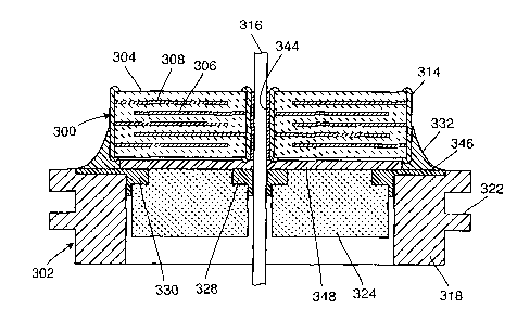
FIGURE 20 illustrates a hermetic terminal 302 which is similar to
the hermetic terminal 202 of FIG. 15, but which has been modified in
accordance with the present invention by extending a gold braze area 346
to create a rectangular pad as shown. The gold braze 346, which runs
around the alumina insulator 324, is also run into two pockets that are
convenient for capacitor mounting.
FIGURE 21 shows a quadpolar feedthrough capacitor 300
(which is identical to the capacitor 200 of FIG. 14) mounted to the hermetic
terminal of FIG. 20. As one can see in FIG. 21, the conductive polyimide
material 332 now connects between the capacitor metallization 314 and
the gold braze area 346. The gold braze forms a metallurgical bond with
the titanium and precludes any possibility of an oxide forming. Gold is a
noble metal that does not oxidize and remains very stable even at
elevated temperatures. The novel construction methodology illustrated in
CA 02446430 2003-11-05
WO 03/073449 PCT/US03/06271
-24-
FIG. 21 guarantees that the capacitor ohmic losses will remain very small
at all frequencies.
FIGURE 22 is a cross-section of the capacitor shown in FIG. 21.
One can see that the gold braze (or weld) areas 328 and 330 that form the
hermetic seal between the alumina insulator 324 and the titanium ferrule
318 are desirably on the feedthrough capacitor side. This makes it easy to
manufacture the gold bond pad area 346 for convenient attachment of the
conductive thermalsetting material 332. In other words, by having the gold
braze hermetic seals on the same side as the gold bond pad area, these
can be co-formed in one manufacturing operation in a gold braze vacuum
furnace. Further, a unique thermalsetting material 348 is disposed
between the capacitor 300 and the underlying hermetic terminal 302.
Another feature of the present invention is that in the prior art
only conductive thermalsetting materials could be used to electrically
connect the capacitor ground metallization 314 to the ferrule 318. This is
because titanium, niobium, tantalum and other biocornpatible materials
used for human implant ferrules are generally not solderable. With the
present invention, it is now possible to replace the thermalsetting
conductive adhesive with solder. Solder paste could also be used. This is
because solder will properly wet and bond to the gold braze area 346.
Solder reflow operations tend to be more cost efficient (more automatable)
as compared to dispensing of thermalsetting conductive adhesives. It
should also be noted that the gold bond pad area 346 of FIG. 21 could be
achieved using other methods. Gold brazing is one method that has
already been described. However, sputter coatings of material surfaces
such as gold, platinum or other conductive materials could be done. In
addition, the gold bond pad area 346 could be done by electroplating of a
suitable material that would form an electrical bond to the titanium and
preclude oxide formation or by any other deposition method capable of
achieving the desired result.
Accordingly, it will be understood that a novel feature of the
present invention is the capability of producing a hermetic seal using noble
CA 02446430 2003-11-05
WO 03/073449 PCT/US03/06271
-25-
materials such as gold braze while at the same time forming a gold bond
pad or landing area to which to connect the capacitor ground metallization.
With specific reference to FIG. 22, the hermetic seal 330 forms a hermetic
braze connection between the ferrule 302 and the alumina insulator 324.
This also, at the same time, forms the gold bond pad 346 for convenient
connection of the conductive polyimide 332. The conductive polyimide
forms the electrical connection between the capacitor ground electrode
plates through the capacitor metallization 314 which connects directly to
the conductive polyimide 332 and to gold bond pad 346.
There are a number of advantages in having the hermetic
connection 330 be co-formed with gold bond pad 346. First of all there is
a very significant manufacturing advantage to having this all done in one
operation. A single gold pre-form can be used, which is formed to
accommodate the area as shown. In addition, this can all be done in one
batch of product put into the vacuum gold brazing furnace at one time. In
a typical manufacturing operation of the hermetic terminal, batches of
parts are placed into carbon/graphite holding/alignment fixtures called
boats, the lead wires and alumina and gold pre-forms along with the
ferrules are then all loaded into this special fixture. The operator then
places these in a sealed chamber known as a vacuum brazing furnace.
Then over a period of time, the temperature is raised sufficiently to re-flow
the gold braze material. The gold makes a connection between sputtering,
which was formerly placed on the alumina terminal 324 so that good
wetting takes place, and a hermetic seal is formed. There is also a good
wetting to the titanium such that a hermetic seal is formed there also. This
can all be done in one continuous operation wherein the gold only wets to
the titanium in the selected areas where the conductive polyimide 332 is to
be placed. Accordingly, the structure as shown in 332 in FIG. 22 can all
be formed in one manufacturing step with very little added cost. There is
also an electrical advantage to doing it this way. By extending the gold
bond pad over the greater area to include the hermetic seal portion of the
gold braze, there is additional contact area of the gold to the titanium
CA 02446430 2003-11-05
WO 03/073449 PCT/US03/06271
-26-
thereby further lowering the contact resistance related to the formation of
oxides as previously mentioned herein. It has been demonstrated that the
formation of these oxides can reduce the effectiveness of an EMI filter at
high frequency. This is because the titanium oxide would increase the
capacitor's equivalent series resistance thereby adding an undesirable
resistance in series with the bypass capacitor.
Speaking specifically to U.S. Patent No. 5,867,361 (Wolf, et al)
dated February 2, 1999, FIG. 1 of the Wolf patent discloses a gold braze
40 for connection of the conductive polyimide 47 to the titanium ferrule.
Wolf indicates that the insertion loss or high frequency performance of the
EMI filter is improved by connection to this gold bond pad. FIG. 9
illustrates the attenuation in decibels with and without a gold bond pad 40.
In the Wolf patent, the hermetic seal is made between the alumina
insulator using a gold braze shown in FIG. 1 as Item 15. The gold braze
15 connects between the ferrule 93 and the alumina insulator 25. There is
also a hermetic and electrical connection made between the lead wire 29
and the alumina insulator through gold braze 90. It is significant that the
entire hermetic seal is formed in this lower region of FIG. 1. The
attachment to the filter capacitor 50 is made using conductive polyimide 47
which is attached to the ferrule 93 by way of the gold brazed material 40.
In the Wolf patent, the gold braze material is an area completely separate
and distinct from the gold braze material 15 which is used to form the
hermetic seal. Accordingly, this is done in two operations or two steps
involving two separate gold brazed pre-forms. There is no hermetic seal
between the ceramic capacitor 50 and the ferrule 93. In fact, any material
used to make electrical connection between the ceramic capacitor and the
ferrule is described as a conductive thermalsetting material, such as a
silver filled polyimide or a solder or the like. None of these are suitable
biocompatible sealing materials for human implant applications and they
certainly do not make a hermetic seal (nor does solder since it is not
considered a biocompatible material).
CA 02446430 2003-11-05
WO 03/073449 PCT/US03/06271
-27-
It is a novel feature of the present invention, as shown in FIG.
22, that the hermetic seal and the gold bond pad is integrated into a single
monolithic structure.
FIGURE 23 illustrates a surface mounted quadpolar feedthrough
capacitor 400. A gold braze bond pad area 446 has been added to
facilitate the connection between the capacitor outside diameter
metallization 414 and the titanium ferrule 418. As mentioned before, this
connection can be made as in the past with a thermalsetting conductive
adhesive 432 or with solder or the like.
FIGURE 24 is a cross-section of the quadpolar feedthrough filter
capacitor terminal of FIG. 23. The gold braze area 446 or optionally 446'
has been extended and widened so that the capacitor outside diameter
electrical connection 432 will touch off between the capacitor outside
diameter metallization 414 and the gold braze surfaces 446 or 446'. By
having an electrically conductive metallurgical joint directly between the
capacitor metallization and the gold braze, there is no chance for any
titanium oxide build-up to affect the capacitor's performance.
Another inventive concept illustrated in FIG. 24 is the electrical
connection 444 between the lead wires 416 and the capacitor metallization
410 and gold braze 428, 428'. This has been made possible by use of a
thermalsetting insulative material 448.
A unique design constraint affecting filtered hermetic terminals
for implantable medical devices is that these devices are designed to be
welded into the overall titanium housing of a pacemaker, implantable
defibrillator or the like. Accordingly, the feedthrough capacitor assembly is
subjected to a great deal of heat and thermal stress. Thus, the insulative
material 448 has to withstand very high temperature. One such insulative
material 448 is a unique thermal plastic polyimide supportive tape (coated
with thermalsetting adhesive) manufactured by Ablestik Electronic
Materials and Adhesives, (the mechanical properties of which are listed in
FIG. 25.) This material, which is known as Ableloc 5500, is unique in that
it has the high temperature characteristics of a polyimide and yet will not
CA 02446430 2003-11-05
WO 03/073449 PCT/US03/06271
-28-
flow. In other words, it stays in place, which allows one to form the novel
structure shown at 448.
It is very important that the bottom or the surface between the
capacitor 400 and the alumina insulator 424 be sealed so that conductive
materials or fluids cannot run between the capacitor pins and short it out.
The Ableloc 5500 is ideal in that it forms a seal while remaining in place.
This means that for the first time the present invention can guarantee that
the capacitor inside diameter connection can be between the capacitor
metallization 410 and the gold braze 428 or 428', which opens up entirely
new possibilities. . For the first time niobium or tantalum pins can be
utilized, without preparatory and secondary processing operations which
are required because these materials are notoriously covered with oxide.
No longer must there be a direct connection between the capacitor
metallization 410 and the pin 416 itself. Instead, the gold braze 428 or
428', which forms the hermetic seal, makes an oxide free metallurgical and
very low resistance connection to the pin itself (in a one step operation).
Accordingly, the electrical connection 444 between the pin 416 as shown
in FIG. 24 is actually from the capacitor inside diameter metallization 410
directly to the gold braze 428. The presence of oxides on the pin simply
doesn't matter since a very low resistance electrical connection has
already been formed. This electrical connection is also RF tight allowing
the feedthrough capacitor to operate at very high frequency as a proper
EMI filter.
FIGURE 26 represents a prior art feedthrough capacitor 500
typical of U.S. Patent No. 4,424,551 and related patents. The bottom
surface of the capacitor 500 has been flooded with a nonconductive epoxy
550. As exemplified in U.S. Patent No. 4,424,551, the insulative material
550 is cured so that the capacitor 500 is bonded into the case 518.
Subsequent to this, the entire surface above the capacitor 500 is flooded
with conductive polyimide material 532, which is then centrifuged into
place. It is very important during the centrifuge operation that material not
flow underneath the capacitor thereby forming a short between the ferrule
CA 02446430 2003-11-05
WO 03/073449 PCT/US03/06271
_29_
and the capacitor inside diameter pin 516. An optional insulative epoxy
coating 552 could be added to cosmetically cover the surface of the
capacitor 500 and offer it some degree of mechanical protection. As can
be seen in this prior art assembly, there is no way for the conductive
polyimide 544 at the inside diameter to reach the gold braze 528. Also, it
is not possible for the outside diameter conductive polyimide 532 to reach
the gold braze 530. This type of prior art assembly is sensitive to any type
of titanium oxide build-up that may occur on the inside diameter of the
titanium ferrule.
FIGURE 27 illustrates another prior art feedthrough capacitor
600 and related structure. This unit has a substantial oxide layer 634 on
the inside of the titanium ferrule 618. For simplicity, this oxide layer is
only
shown on the inside diameter of the ferrule 618 where the electrical
connection to the capacitor ground metallization 614 is made (in actual
practice, the oxide would to some degree coat all of the ferrule surfaces).
Accordingly, there will be a high resistance between the conductive
polyimide 632 and the titanium ferrule 618. In this case the gold brazes
628 and 630 are shown on the opposite side away from the feedthrough
capacitor 600. Accordingly, there is no way in this structure for the
feedthrough capacitor ground polyimide connection to have contact with
the gold braze 630. Thus, this prior art assembly is subject to EMI filter
performance degradation if the oxide layer becomes too thick. Product life
is another concern. Oxides can build up very slowly over time and lead to
a latent type of design defect.
FIGURE 28 illustrates the novel technology of the present
invention as applied to the basic structures illustrated in FIGS. 26 and 27.
The unique Ableloc 5500 or equivalent high temperature thermal plastic
polyimide supportive tape 748 allows the nonconductive insulating material
to be held in place as shown (B staged epoxy washers could also be used,
however, their temperature rating is not as high). This allows clear access
for the conductive polyimide 744 or 732 to penetrate and contact the gold
braze area 746. In this case, it is important that the gold braze be on the
CA 02446430 2003-11-05
WO 03/073449 PCT/US03/06271
-30-
capacitor side of the insulator 724. The assembly shown in FIG. 28 no
longer requires that the pins) 716 be restricted solely to platinum iridium
or other non-oxidizing materials. This allows the use of much lower 'cost
niobium or tantalum pins. The electrical connection can be between the
capacitor inside diameter metallization 710 directly to the gold braze 728
itself. Accordingly, there is no need for an electrical connection between
the capacitor inside diameter metallization 710 and the lead wire 716 at all.
It can also be clearly seen in FIG. 28 that it would not matter if the inside
diameter of the ferrule 718 was heavily oxidized. This is because there is
an electrical connection directly from the capacitor outside diameter
metallization 714 to the outside diameter gold braze 730.
FIGURE 29 is a broken out enlarged view of the outside
diameter connection of FIG. 28. As one can see, there is an oxide layer
734 which would tend to insulate the conductive polyimide or solder 732
from the titanium. However, because of the proper location of insulative
material 748, the conductive polyimide, solder or the like 732 can make
direct contact between the capacitor metallization 714 and the gold braze
area 730. Sputtering 754 of metals on the alumina insulator 724 are
required before the gold braze hermetic seal typically can be formed. This
allows the gold braze material 730 to wet to the alumina insulator 724 and
° form a hermetic seal.
FIGURE 30 is an enlarged view of the electrical connection to
the lead wire 716 of FIG. 28. It is assumed that a type of lead wire is
used, such as tantalum or niobium, which would be heavily oxidized 734.
Not only are these oxides highly insulative, but they also do not form a
solderable surface. However, a feature of the invention is that during
hermetic seal construction, the oxides are absorbed by the metallurgical
bond formed between the gold braze area 728 and the pin 716. This is the
same gold braze that forms the hermetic seal to the alumina insulator 724.
A sputtered layer 754 allows the gold to wet to the insulator 724. As one
can see, no direct connection between the capacitor metallization 710 and
the lead wire 716 is required. Instead, the connection to the capacitor is
CA 02446430 2003-11-05
WO 03/073449 PCT/US03/06271
-31 -
accomplished by the thermalsetting conductive adhesive or solder 744
which connects from the capacitor metallization 710 directly to the gold
braze 728. Since the gold braze 728 has a metallurgical low resistance
and low impedance connection to the pin, no further connection is
required. In the case of a non-oxidizing pin material such as platinum,
gold or platinum-iridium alloy, it is not necessary to form the structure as
illustrated in FIG. 30. In other words, the insulative washer 748 could
extend all the way across the inside diameter thereby blocking access to
the gold braze.
The most critical element in a medical implant feedthrough
design (that must remain hermetic throughout it's device service life) is the
metal/ceramic interface. Important are the nature of the bond itself and
the sensitivity of the bond integrity to environmental conditions imposed as
a result of the device fabrication process (like installation by laser welding
by the pacemaker manufacturer) or as a part of environmental conditions
developed while in service (body fluid is highly corrosive). For a braze-
bonded feedthrough, the bond needs to deform in a ductile manner when
environmental conditions create stresses (e.g., heating and cooling cycles
that develop during device assembly welding). Typically, metallization and ~~
braze material combinations develop alloys that solidify as intermetallics.
These intermetallics often show only modest ductility prior to failure. If
material combinations are not judiciously selected and processes are not
understood and controlled, significant dissolution can occur, and brittle
fracture of the bond, or latent failures (static fatigue) result compromising
hermetic integrity of the feedthrough.
A unique challenge for formation of the novel bond~pads of the
present invention is that they are formed as an integral part of the hermetic
seal joint. This requires a relatively large amount of gold braze material
(or other noble metal) to be used. In prior art EMI filtered human implant
hermetic seals, the volume of braze material is by design relatively small.
In the present invention, with the larger volume of braze material that is
required, higher stresses due to shrinkage and mismatches in the thermal
CA 02446430 2003-11-05
WO 03/073449 PCT/US03/06271
-32-
coefficient of expansion (TCE) of the braze material become a major
design challenge. The biggest concern is the added stress in tension or
shear which is transmitted to the metallic layer on the alumina hermetic
seal/insulator (this layer is what allows the braze material to wet to the
alumina and form the hermetic seal and is preferably applied by sputtering
or equivalent methods). Unfortunately, the TCE of the high alumina
content ceramic insulator does not match the TCE of any of the noble
metal braze materials. Accordingly, for formation of the novel integrated
gold hermetic seal/bonding pad as described herein, a unique metallization
is required to be used in combination with the present invention that has
high malleability and very high adhesion strength to the alumina ceramic
and will also wet well to the braze material. It is a feature of the present
invention that the preferred metallization on high alumina ceramics for
miniature medical implantable device hermetic terminals, is
titanium/molybdenum. Titanium is the active layer, and molybdenum is the
barrier layer controlling how much titanium can actually dissolve in the
gold. For example, 2-4 microns of titanium can be sputtered followed by
2-4 microns of molybdenum. The thickness will be dependent on the
design, the application, and the subsequent potential environmental
exposures. In this example, the titanium layer provides the interaction with
the glass phases and alumina particle matrix of the ceramic to create a
hermetic bond. The molybdenum layer protects the titanium layer from
excessive oxidation prior to brazing and acts as a barrier between the gold
braze material and the titanium layer. Without the molybdenum barrier
layer, an excessive length of exposure of the titanium layer to the molten
gold would accelerate the inherent alloying process and eventually lead to
de-wetting, then hermetic failure
The titanium/molybdenum metallization in concert with gold
braze, therefore, not only provides a sound hermetic bond, but also
provides a sufficiently ductile materials feedthrough system to sustain
secondary device assembly processes or environmental conditions that
might develop stresses while the device is in service.
CA 02446430 2003-11-05
WO 03/073449 PCT/US03/06271
-33-
Other metallization materials that can be used with gold braze
materials include but are not limited to titanium, niobium, chromium,
zirconium, or vanadium active materials with molybdenum, platinum,
palladium, tantalum or tungsten barrier layers in various combinations.
Sputtering is one metallization application method. Other methods that
might be used include but are not limited to chemical vapor deposition,
laser or other physical vapor deposition processes, vacuum evaporation,
thick film application methods, plating, and so on.
FIGURES 31-36 illustrate an internally grounded bipolar
rectangular feedthrough capacitor 800 as described in U.S. Patent No.
5,905,627. The center hole is the grounded hole 858 which would connect
to the capacitor internal electrode plates 808. More specifically, the
feedthrough filter capacitor 800 comprises a monolithic, ceramic internally
grounded bipolar feedthrough filter capacitor having three passageways
extending therethrough. The outer two passageways 856 are configured
to receive therethrough respective conductive terminal pins 816' and 816",
and the internal diameter of the first passageways 856 are metallized 810
to form a conductive link between the active electrode plates 806. As is
well understood in the art, the active electrode plates 806 are typically silk-
screened onto ceramic plates forming the feedthrough filter capacitor 800.
These plates 806 are surrounded by an insulative ceramic material 804
that need not be metallized on its exterior surfaces.
Similarly, ground electrode plates 808 are provided within the
feedthrough filter capacitor 800. The inner diameter of the central or
second passageway 858 through the feedthrough filter capacitor 800 is
also metallized 811 to conductively connect the ground electrode plates
808, which comprise the ground plane of the feedthrough filter capacitor
800. The second passageway 858 is configured to receive therethrough
the ground lead 860 which, in this particular embodiment, comprises a
ground pin.
With reference to FIG. 32, the terminal pin subassembly
comprises a plate-like conductive ferrule 818 having three apertures
CA 02446430 2003-11-05
WO 03/073449 PCT/US03/06271
-34-
therethrough that correspond to the three passageways through the
feedthrough filter capacitor 800. The conductive terminal pins 816' and
816" are each supported through the outer apertures by means of an
insulator 824 (which also may be hermetic), and the ground pin 860 is
' supported within the central aperture by a suitable conductor 830 such as
gold brazing, solder, an electrically conductive thermalsetting material or
welding/brazing.
The feedthrough filter capacitor 800, as shown, is placed
adjacent to the non-body fluid side of the conductive ferrule 818 and a
conductive attachment is effected between the metallized inner diameter
of the first and second passageways 856 and 858 through the feedthrough
filter capacitor 800 and the respective terminal pins 816 and ground lead
860. Alternatively, the capacitor 800 could be placed adjacent to the body
fluid side of the conductive ferrule 818 provided the capacitor comprises a
design incorporating biocompatible materials. In FIG. 35, the conductive
connections 844 between the terminal pins 816 and the ground lead 860,
with the feedthrough filter capacitor 800 may be effected by any suitable
means such as a solder or an electrically conductive thermalsetting
material or brazing. The result is the feedthrough filter capacitor assembly
illustrated in FIGS. 35 and 36 which may then be subsequently laser
welded into the titanium housing of an implantable medical device.
FIGURE 35 illustrates the internally grounded bipolar
feedthrough capacitor 800 of FIG. 31 mounted to the hermetic feedthrough
terminal 802 of FIG. 32. The ground lead 860 can be shortened so that it
does not protrude through the capacitor 800 or it can be lengthened
depending on whether or not a circuit attachment is required within the
implantable medical or other electronic device. If the lead wires are
solderable (platinum or gold), then the connection between the lead wires
and the capacitor inside diameter metallization can be accomplished using
solder, conductive adhesive or the like. A feature of the internally
grounded feedthrough capacitor 800 is that no outside diameter (or
CA 02446430 2003-11-05
WO 03/073449 PCT/US03/06271
-35-
perimeter in the case of FIG. 35) electrical connection or capacitor
metallization is required.
FIGURE 36 is a cross-section of the capacitor assembly of FIG.
35. This illustrates several novel features of the present invention that are
applicable to the internally grounded feedthrough capacitor, especially
when lead wire materials that are subject to oxidation are used (such as
niobium or tantalum). As one can see, the thermal plastic polyimide
supportive tape 850 has been carefully punched, die-cut, or laser cut to
align with the capacitor such that the capacitor feedthrough holes are open
to the gold braze material 830 underneath. This allows a direct connection
of the solder or conductive polyimide 844 to connect directly between the
capacitor metallization 810, 811 and gold braze material 830. Accordingly,
this opens up a wide variety of lead materials for use, which could not be
considered before due to their heavy oxidation or poor solderability
properties. This also allows the use of a ground pin of alternate materials,
like titanium. A titanium ground pin is desirable because it is very easy to
weld a titanium pin into a titanium ferrule. In the past, it was not possible
to solder directly to titanium, however, a feature of the present invention is
the capability of connection to the gold braze area. It should be apparent
that not all leads are required to be constructed of the same material. For
example, the center (ground) lead 860 could be titanium and the two
active pins 816' and 816" could be platinum. In this case, it would not be
required that conductive material 844 adjacent the platinum pins 816' and
8'16" contact the gold braze 830.
FIGURE 37 illustrates a novel hybrid capacitor 900 which has
the characteristics of a conventional surface mounted feedthrough
capacitor and an internally grounded capacitor. This capacitor 900 has a
ground hole 958 in the center which connects to the internal ground
electrode plates 908 and also has ground terminations 914 at either end.
The reason for this is that this capacitor has a form factor which tends to
increase its inductance and impedance. Accordingly, if one were to only
make connection to the ground electrodes 908 shown in FIG. 38 at the
CA 02446430 2003-11-05
WO 03/073449 PCT/US03/06271
-36-
center hole 958, there would be too much inductance between this and the
outer pins to perform effective EMI filtering. This hybrid design is best
illustrated by the ground electrode plate pattern as shown in FIG. 38,
wherein the ground electrode 908 is attached to the titanium ferrule 918 at
both the right and left ends and also in the middle. This guarantees that
the capacitor 900 will have very low impedance across its entire ground
plane thereby ensuring that it will work properly as a high frequency EMI
filter. FIGURE 39 is an illustration of the active electrode plate pattern
906.
FIGURE 40 illustrates the simplified hermetic terminal 902. The
centered ground pin 960 is welded or brazed 928 directly to the ferrule
918. This forms a low resistance and low inductance ground connection to
the pin 960. The other pins 916 are shown in insulative relationship with
the ferrule 918. The novel gold bond pads of the present invention are
shown as 946. Restated, the ground pin 960 has been solidly brazed
directly to the ferrule 918. This provides a very low impedance RF ground
between the center pin 960 and the overall electromagnetic shield. One
can also see in FIG. 40 that the gold bond pads 946 have been added on
either end to form a convenient surface for the electrical connection
between the capacitor end terminations 914 and the ferrule 918. It can
also be seen that the other four pins 916 on both the right and left sides of
the capacitor 900 are in electrically insulative relationship. This is done
through the insulators 924 which can be glass or a gold brazed alumina
seal.
FIGURE 41 is a top view of the capacitor of FIG. 37 mounted to
titanium ferrule 918. The novel gold braze ground pads 946 of the present
invention have been added so that an oxide free electrical connection can
be made between the capacitor-ground terminations 914 and the
conductive ferrule 918.
FIGURE 42 is a cross-sectional view of the capacitor 900
assembled to the hermetic terminal 902 of FIG. 40. As shown, the gold
bond pads 946 are also part of a single monolithic structure forming the
CA 02446430 2003-11-05
WO 03/073449 PCT/US03/06271
-37-
hermetic seal between the ferrule 918 and the insulator 924, in the same
manner and for the same reasons as discussed above in connection with
FIG. 22. The connection between the capacitor ground metallization 914
(at its two ends) and the gold bond pads 946 is shown as material 932,
which can be solder, conductive thermalsetting material, or the like. The
connection to the centered ground pin 960 is illustrated by material 944
which can also be solder, conductive thermalsetting material, or the like.
As previously mentioned, in the present invention it is desirable to form
insulative material 948 such that the electrical connecting material 944
adjacent to the ground pin 960 will directly contact the gold braze 928.
This is particularly important for ground pin lead materials that are not
readily solderable or that form insulative oxide layers. The novel gold
bond pad area 946 as previously mentioned could also be accomplished
by sputtering, plating and the like.
As illustrated in FIG. 42, for comparison purposes, the hermetic
terminal 902 includes two distinctly different sets of lead wires 916. To the
left of the ground pin 960, the lead wires 916 are shown as comprised of
low cost niobium or tantalum pins on which heavy oxides typically form.
When utilizing such low cost pins, the pads of oxide resistant conductive
biostable material, noble metal, or the like, 946 are utilized to provide both
a hermetic seal between the pins and the insulator 924, and also to
provide a reliable electrical connection between the interior termination
surfaces 910 and the leads 916, as discussed above in connection with
FIGS. 24, 28-30 and 36. In contrast, the lead wires 916 to the right of the
ground pin 960 are all platinum. As a noble metal, platinum is not subject
to oxidation. Accordingly, it is not necessary for the solder or conductive
polyimide used to connect between the capacitor inside diameter
metallization and the lead wire to also contact the gold braze material 928.
In other words, an oxide free electrical connection has already been made
between the capacitor inside diameter metallization 910 and the lead wire
916, therefore it is not necessary to modify this assembly to contact the
gold braze. However, in accordance with the invention, the
CA 02446430 2003-11-05
WO 03/073449 PCT/US03/06271
-38-
aforementioned polyimide supportive tape 948 or the like could be placed
to allow direct contact from the ground pin 960 to the gold braze 930
thereby allowing the use of a ground lead wire such as titanium, niobium
or tantalum.
FIGURE 43 shows a hybrid capacitor 1000 which has a
centered ground pin 1060 and, because of its length and the desire to
reduce inductance, is also grounded at its right and left ends using
conductive polyimide 1032 to the gold bond pads 1046. This is a hybrid in
that it incorporates the features of both U.S~ Patent Nos. 5,333,905 and
5,095,627. FIG. 43 illustrates novel wire bond pads that overcome all of
the obvious deficiencies of the aforementioned Wolf patent. The preferred
location for the hermetic braze between the insulators 1024 and the
hermetic terminal 1002 is at the pads 1046. This takes the gold braze
away from the body fluid both at each terminal pin and also at the hermetic
seal joint to the ferrule. When a header block, which is commonly used in
the industry is attached, silicone or other material is utilized which will
fill
the space between the lead all the way down to the gold braze. This
effectively blocks the ready access of body fluids to the gold braze thereby
preventing reverse electroplating involving material deposition to some
other surface in the presence of a voltage bias. In other words, the
location of the hermetic seal shown in FIG. 43 will overcome any problem
with long term exposure to body fluid.
FIGURE 43 and 44 further illustrate an extruded nail head lead
1016 of bio-compatible material such as a noble metal including platinum,
platinum iridium, gold and the like. The nail head portion 1062 of the lead
1016 on the bottom or body fluid side could be extruded as one piece
particularly with a malleable material welded in place, brazed in place, or
adhesively secured in place to the lead 1016. The capacitor 1000 is
attached to the terminal 1002 using similar processes as described above,
and the leads 1016 are attached at the time that the hermetic seal joint
1046 is formed. During capacitor attachment the leads 1016 are allowed
to stick through the capacitor 1000 as shown. At this point there are a
CA 02446430 2003-11-05
WO 03/073449 PCT/US03/06271
-39-
number of options for the assembly. One option would be to make a
solder joint, braze, weld or a thermalsetting conductive adhesive joint 1099
between the capacitor inside diameter termination and the nail head
terminal pin 1016. One could then add a wire bond closed pad or cap
1064 and attach it by soldering, welding, thermal conductive adhesive
brazing or the like 1098. The wire bond pad 1064 does not need to be bio-
compatible and could be made of a, number of inexpensive materials
including nickel, copper, steel and the like. For wire bond applications it is
usually required that the wire bond pad 1064 be pure (soft) gold plated, but
a number of other surface finishes can be applied as well. The wire bond
pads/nail head assembly 1016, 1064 could also be formed from the group
of metals including: tantalum, molybdenum, titanium, rhodium, titanium
alloys, osmium, silver and silver alloys, vanadium, platinum, niobium,
platinum alloys, stainless steel, tungsten, rhenium, zirconium, vanadium
and ruthenium.
FIGURE 45 illustrates an internally grounded hex polar capacitor
1100 embodying the invention (refer to U.S. Patent No. 5,905,627). In this
particular device, the novel wire bond pads 1164 as previously described
have been utilized. The nail head pin 1116 is of the same group of
materials as previously described for FIG. 43. However, in this
embodiment the hermetic seal 1146 has been moved to an alternate
location and is now closer to exposure to body fluids. This is also
acceptable to many customers but is not the preferred embodiment for
maximum resistance to long term decomposition by metal migration.
The wire bond pad 1164 on the inside of the implantable
medical device has also been modified so it has an open hole. In this
case this a ring structure which is slipped over the bio-compatible pin 1116
and then attached by soldering, welding, brazing, or thermalsetting
conductive adhesive or the like. An advantage of this structure is it is a
little bit easier to assemble and inspect. A disadvantage is that the area
available for customer attachment of their lead wires by ultrasonic wire
bonding, thermal sonic welding or direct welding has been reduced. In
CA 02446430 2003-11-05
WO 03/073449 PCT/US03/06271
-40-
other words there is less flat surface area available for customer lead
attach.
Referring to FIG. 47A, a different embodiment of attachment of
the lead wire 1160 is shown. In this case the lead wire 1160 extends
through a toroidal ring 1164' which may be constructed of various
materials from the group of metals, and ceramics. One preferred
embodiment would be the use of alumina ceramic which was metallized.
This would allow one to form the electrical connection shown while at the
same time allowing the lead wire 1160 to protrude through. In this case
the very end of the lead wire 1160 could be the wire bond pad itself.
There are a number of supplementary processes available after the
extrusion of this lead wire to provide a flat and parallel surface. This has a
number of advantages that will be obvious to one skilled in the art
including the ability to readily inspect the joints.
More particularly, the preferred metallized alumina toroidal ring
1164' has been metallized on all surfaces so it is both solderable and
conductive. Solder, thermalsetting conductive adhesive, welding or the
like 1168 performs an electrical connection between the circular torroid
1164' which in turn connects to the capacitor 1100 active electrode plates
1106. In addition, material 1170, which can be of the group of solder,
thermalsetting conductive adhesives, welding, brazes or the like, forms the
electrical connection between the lead wire 1160 to the torroidal structure
1164' which then couples through the electrical connection 1168 via the
capacitor metallization 1110 to the electrode plates. As shown the tip of
the lead wire 1172 is flat to accept lead attachment by the customer by
wire bonding, thermal sonic bonding, laser welding or the like. A
supplementary nail head or enlarged area could be added to the tip 1172
to increase the surface area available for such customer lead attachment
operations. One particular advantage of the structure shown in FIG. 47 is
the ability to select a material that closely matches a thermal co-efficient
expansion of the ceramic capacitor 1100. Such materials include fosterite,
zirconium, gold alloys, or materials such dumet.
CA 02446430 2003-11-05
WO 03/073449 PCT/US03/06271
-41 -
Capacitor 1100 has inside diameter metallization 1197 at each
of the seven inside diameters to make electrical connection to the ground
and active electrode plate sets. This metallization also appears on top of
the capacitor as a circular mountinglbonding pad 1199. In this case, there
is no need to fill the space between the capacitor inside diameters and the
noble metal lead wires with an electrical connection material.
FIGURE 47B shows that the lead wire and its electrical
connection may be subflush or below the top of the ring pad 1164. In this
case, the ring pad forms the wire bond surface.
As shown in FIG. 47C, the electrical connection is formed
between pin 1116 and the capacitor top metallization 1199 using solder,
braze, conductive adhesive or the like. Alternative connections using a
variety of wire bond pad end caps are shown in FIGS. 47A, 47B, and 47C.
FIGURES 48 and 49 show an externally grounded quadpolar
device. While a compatible nail head pin 1216 is utilized and in this case,
the hermetic seal connection 1246 between the alumina ceramic 1224 and
the nail head pin 1216 is in the preferred location. Drawing attention now
to the wire bond end cap 1264, a different attachment method is
contemplated. This attachment method is desirable in that it completely
eliminates the necessity for any contact materials or any solder or other
materials to be placed between the lead wire 1216 and the inside diameter
termination of the ceramic capacitor 1200. In this case the capacitor 1200
inside diameter metallization 1210 is also formed as a circular structure on
the top surfaces of the ceramic capacitor. This is commonly used in the
connector.industry and with planar arrays. Such structures are normally
printed on the top surface of the ceramic capacitor by silk screening
processes or the like. Accordingly, it is easy to form this on the top
surface of the capacitor 1200. This makes the attachment of the end cap
1264 very simple and easy to facilitate in a manufacturing operation. As
best seen in FIG. 49, attachment of the wire bond cap 1264 is simply
accomplished by making a solder joint, conductive thermalsetting adhesive
joint, braze joint, weld joint or the like shown as 1266. This makes a direct
CA 02446430 2003-11-05
WO 03/073449 PCT/US03/06271
- 42 -
connection to the capacitor termination 1210. Accordingly, there is no
other connection to the capacitor inside diameter that is needed. At the
same time that the joint 1266 is formed or at a different time, the electrical
connection 1299 to the end cap 1264 is also made. As previously
mentioned, this can be done thermalsetting conductive adhesives, solder,
brazes, welds or the like.
This is a major advantage over the aforementioned iNolf patent
in that the inside diameter of the capacitor does not have any materials
that mis-match it in its thermal co-efficient of expansion. Accordingly, the
capacitor will be mechanically more rugged and more resistant to thermal
shock such as those induced by the customer during installation by laser
welding. The capacitor termination materials are preferably in this case
formed from either plating or a fired on silver or a palladium-silver glass
frit. These are put on as a thick film process sufficient so that it forms a
mechanically rugged and electrically reliable attachment to the capacitor
active electrode plates 1206.
Although several embodiments of the invention have been
described in detail for purposes of illustration, various modifications of
each may be made without departing from the spirit and scope of the
invention. Accordingly, the invention is not to be limited, except as by the
appended claims.