Note: Descriptions are shown in the official language in which they were submitted.
CA 02447348 2003-11-10
WO 03/003421 PCT/US02/20699
TITLE
Optical Chip Packaging Via Through Hole
FIELD OF THE INVENTION
The present invention relates to optical chips and, more particularly, to
optical chip
packaging.
CROSS REFERENCE TO RELATED APPLICATIONS
This application claims priority under 35 USC 119(e)(1) of United States
Provisional
Patent Application Serial No.60/302,578 filed June 29, 2001.
This application is also a continuation in part of commonly assigned United
States
Patent Applications Serial Nos. 09/896,189, 09/897,160, 09/896,983, 09/897,158
and
09/896,665, all filed June 29, 2001.
BACKGROUND
As set forth herein, items in the figures are referred to in the format #1 -
#2 where #1
denotes the figure and #2 denotes the item in that figure. For example, 9-213
means item 213
in figure 9.
Opto-electronic chips have the ability to provide huge optical bandwidth.
However,
that data sent or received optically needs to get into and out of the chips
electrically. Thus,
the amount of electronic I/O needs to be large so as not to unduly create a
bottleneck in the
flow of data. Given the constraints on how fast an individual electrical line
can be, the
requirement for a large amount of I/O typically translates into a large number
of I/O pads on
the chip. However, the ability to place many electrical I/O connections a chip
is
counterbalanced by the need to place the I/O connections as close together as
possible.
Typically, users of optical modules (containing one or more opto-electronic
chips) or
designers of components on which those modules mount, like to have the modules
configured
so that the modules will mount onto circuit boards and have the electrical I/O
connections at a
90 degree angle to the optical I/O connection. Thus, it is desirable to allow
the electrical
signals to traverse a 90 degree bend.
Moreover, to the extent optical or opto-electronic chips are connected to flex
circuits,
they are typically connected using wirebonding techniques. Such techniques
introduce
undesirable parasitic capacitance, which is particularly detrimental to high
frequency
operation.
CA 02447348 2003-11-10
WO 03/003421 PCT/US02/20699
Since a goal with these modules is to bring data in and out as quickly as
possible, it is
important to ensure that the speed of each of the electrical connections to
the chip can support
the highest bandwidth (i.e. data rates) possible.
The use of flexible circuits to make 90 degree electrical turns to allow
electrical
access to occur at a right angle to optical access per se is known, for
example, from D.
Pommerrenig, D. Enders, T. E. Meinhardt, "Hybrid Silicon Focal Plane
Development: an
Update," SPIE Vol 267, Staring Infrared Focal Plane Technology, (19~ 1) at p.
23. This
reference describes an approach for soldering or welding cables to the
backside of an optical
chip for 90 degree turning. A chip produced using the prior art approach is
shown in FIG. 1.
Illustrated is a detector 1-2, a flex chip 1-4, a module base 1-6 and a MUX
chip 1-10.
However, the approach suffers from the same problems noted above, as is
evident in FIG. 1,
namely providing optical access inhibits access to the device for cooling.
More recent attempts have followed the same basic approach, but have
electrically
connected the electronic chip to the flex circuit using wirebond techniques,
for example, as
done with Agilent Technologies PONI-1 POSA Package, or using other edge
connecting
metalized connections, for example, beamleads.
All the foregoing approaches however have used a single-side access flex
circuit.
In addition, because wirebonds axe used in the prior art, the use of wirebonds
limits
the number of electrical connections possible between the electronic chip and
the flex circuit
(since the wirebonds require a larger electrical attachment area than a
corresponding number
of connections using flip-chip connection techniques. Wirebonds or other
extended metal
connectors coming off a chip also have large capacitances and inductances
which limit the
speed of the off chip connection and also increases the electrical
crosstalk/noise between
adjacent electrical channels.
FIG. 2 shows one such example of a flex circuit arrangement that allows the
optical
devices to be placed on top of the electronic chip, but the configuration is
still limited by off
electronic-chip wiring and still inhibits access to the non-active side for
cooling. Illustrated
in FIG. 2 is an optional auxiliary chip 2-12, a chip to flex connection 2-14
an electronic chip
2-16 and an optical device 2-20.
Presently, there is no way to package an optical chip or an optical chip with
an
electronic chip (i.e. create an opto-electronic chip) that allows for close
connections between
the two, reduces parasitic capacitance and inductance, provides unobstructed
optical access
while allowing for connection of a heatsink to the chip for cooling.
2
CA 02447348 2003-11-10
WO 03/003421 PCT/US02/20699
SUMMARY OF THE INVENTION
Our invention involves an approach to the integration of optical or opto-
electronic
chips with electrical connectors.
Our approach circumvents the need for off chip electronic wiring or electrical
lead-
oriented connection approaches. Note that the flex prior art of circuit FIG. 2
exists to the
right-side of the electronic chip. Hence it is difficult, if not impossible,
to effectively attach a
heatsink to aid in cooling the electronic chip, since it can not be placed on
the front of the
chip without impeding optical access and it cannot be attached to the back of
the electronic
chip (on the rightside of the chip of FIG. 2 because the flex circuit is in
the way.
One advantage obtainable in accordance with the invention is the approach
allows
high density, high speed, electrical connections to be made to dense opto-
electronic chips
while allowing optical access to those chips.
Another achievable advantage is the ability to provide the above high speed
connections while still allowing for easy optical access for edge-mounted
optical
components.
Advantageously, since the optical component community is moving toward (or
already uses) flex circuits to connect optical modules to circuit cards, our
technique does not
"buck the trend" but rather goes along with so as to allow for greater
acceptance.
In addition, this technique provides the ability to integrate electronic I/O
pads on
optoelectronic chips in multi-tiered rows. Still further, this technique
allows the multi tiered
rows to even be away from the optical or opto-electronic chip edge.
Still further, our technique minimizes parasitic electronic capacitance and
inductance
on flex circuit-to-chip connections.
In addition, the technique of placing the optical or opto-electronic chip on
the
backside of the flex allows for easy heat sink access to the chip without
impeding or
interfering with the optical path, irrespective of whether the chip contains
topside active or
backside (also called bottom) active (also called bottom active) devices.
The advantages and features described herein are a few of the many advantages
and
features available from representative embodiments and are presented only to
assist in
understanding the invention. It should be understood that they are not to be
considered
limitations on the invention as defined by the claims, or limitations on
equivalents to the
claims. For instance, some of these advantages are mutually contradictory, in
that they cannot
be simultaneously present in a single embodiment. Similarly, some advantages
are applicable
to one aspect of the invention, and inapplicable to others. Thus, this summary
of features and
3
CA 02447348 2003-11-10
WO 03/003421 PCT/US02/20699
advantages should not be considered dispositive in determining equivalence.
Additional
features and advantages of the invention will become apparent in the following
description,
from the drawings, and from the claims.
BRIEF DESCRIPTION OF THE DRAWINGS
FIG. 1 shows a chip and flex circuit according to a prior art approach;
FIG. 2 shows one prior art example of a flex circuit arrangement;
FIG. 3 shows, in perspective, an example of a dual side flex circuit in
accordance with
the invention;
FIG. 4 shows another example implementation in accordance with the teachings
of
the invention;
FIG. 5A shows a top view of an example double sided flex circuit with a
through-hole
for use in accordance with the invention;
FIG. 5B shows a side view of the flex circuit of FIG. 5A;
FIG. SC shows a side view of an alternative variant of the flex circuit of
FIG. 5A;
FIG. 6 illustrates approaches that have been used in the prior art to attach
multiple
bottom emitting devices to form an integrated electro-optical chip ;
FIG. 7 illustrates approaches that have been used in the prior art to attach
multiple
bottom emitting devices to form an integrated electro-optical chip;
FIG. 8 illustrates a single optical device with contact pads placed in the
position
specified by its manufacturer and a portion of an electronic wafer with
contact pads placed in
the position specified by its manufacturer;
FIG. 9 illustrates a single optical device with contact pads placed in the
position
specified by its manufacturer and a portion of an electronic wafer with
contact pads placed in
the position specified by its manufacturer of which each will not be aligned;
FIG. 10 illustrates in simplified high level overview, one example approach
according
to the teaches of the invention;
FIGS. 11 and 12 illustrates several different access way variant examples;
FIG. 13 illustrates an optical array in which fibers are supported by the
substrate;
FIG. 14 illustrates an optical array that accommodates an array of
microlenses;
FIG. 15 illustrates one example process for creating an electro-optical chip
variant
according to the techniques described;
FIG. 16 illustrates one example process for creating an electro-optical chip
variant
according to the techniques described;
4
CA 02447348 2003-11-10
WO 03/003421 PCT/US02/20699
FIG. 17 illustrates one example process for creating an electro-optical chip
variant
according to the techniques described;
FIG. 18 illustrates one example process for creating an electro-optical chip
variant
according to the techniques described;
s FIG. 19 illustrates another opto-electronic device being created in a manner
similar to
the devices of FIGS. 1 s-17;
FIG. 20 illustrates a process usable for bottom active devices;
FIG. 21A illustrates a process usable for topside active devices;
FIG. 21B illustrates the process where the contact holes are coated, but not
filled, and
can assist in alignment;
FIG. 21 C shows an optical chip with its contacts rerouted by patterning
traces on the
substrate to match the contacts on another chip;
FIG. 21D shows the contacts on an electronic chip rerouted by patterning
traces on
the substrate to match the contacts on an optical chip;
1s FIG. 22 illustrates a process similar to that shown in Figure 31A except
that a Garner
is not used;
FIG. 23 illustrates a connection chip or adapter chip used to connect
different devices;
FIG. 24 illustrates another alternative implementation, which is a further
variant of the
adapter or connection chip variant, usable for topside active devices;
FIG. 2sA illustrates the stacking of two or more devices using one of the
techniques
according to the invention;
FIG. 2sB illustrates a modulator stacked on top of a laser using one of the
techniques
according to the invention;
FIG. 26 illustrates an array of, for example, one hundred lasers created using
one of
2s the techniques according to the invention;
FIG. 27 illustrates the steps in creating an array for a DWDM application
using one of
the techniques according to the invention;
FIG. 28 illustrates the process of FIG. 27 from a top view;
FIG. 29 is a flowchart for one example process in accordance with the
invention;
FIG. 30 shows the various components being joined according to the process of
FIG.
29;
FIG. 31 is a flowchart for another example process in accordance with the
invention;
and
s
CA 02447348 2003-11-10
WO 03/003421 PCT/US02/20699
FIGS. 32A-32D show example assemblies constructed in accordance with the
invention according to the teachings described herein.
DETAILED DESCRIPTION
In overview, by allowing the flex circuit to have a through-hole in it and
bonding the
optical or opto-electronic chip to the back side of the flex circuit, for
example, using flip-chip
bonding techniques, a dual-sided flex circuit is created that can have
contacts to the optical or
opto-electronic chip on the backside and contacts for connection to the a
printed circuit board
(PCB) on the front side. One example of such a dual side flex circuit 3-30 in
accordance with
the invention is shown in perspective in FIG. 3. The through-hole allows
optical access to the
optical or opto-electronic chip while the placement of that chip on the back
of the flex circuit
also allows for good thermal contact with the chip to be made for cooling.
Moreover, the
placement achieves the foregoing while allowing for a large numbers of
connections to be
made to the optical or opto-electronic chip via the flex circuit.
Advantageously, our technique works whether the optical devices are topside
active
or back side (bottom side) active, as long as the direction of emission (or,
in the case of
photodetectors receipt) of light is away from the electronic chip to which the
optical devices
are hybridized. In addition, the technique can also be employed in instances
where there is
some element located between the optical devices and the opening, provided
that the element
is optically transparent to the wavelength of light the active device operates
with.
The invention solves the problem by placing optical devices on top of the
electronic
chip, through a hybridization process, for example using one of the techniques
described in
the commonly assigned United States Patent Applications Serial Nos.
091896,189,
09/897,160, 09/896,983 and 09/897,158, all filed June 29, 2001 and entitled
"Opto-Electronic
Device Integration", the detailed description of which axe reproduced below in
the section of
the same title, and bonding the electronic chip directly to a circuit card
which contains a cut-
out opening in it to allow optical access for the optical devices while
providing access to the
electronic chip for cooling. Depending upon the particular case, the bondings
described
herein can be performed using conventional techniques or according to the
technique
described in United States Patent Application Serial Nos. 09/896,665 filed
June 29, 2001 and
entitled "Successive Integration of Multiple Devices Process and Product", the
detailed
description of which is reproduced below in the section of the same title.
As a result, signals can be brought out from the chip through a double side
access
circuit card to a conventional set of electrical I/O pads that can be used to
attach the module
6
CA 02447348 2003-11-10
WO 03/003421 PCT/US02/20699
to a printed circuit board. By doing direct integration, performance and cost
limitations
associated with wiring or using other electrical attachment mechanisms are
reduced or
dispensed with entirely.
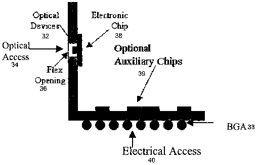
FIG. 4 shows another example implementation in accordance with the teachings
of
S the invention. As shown in FIG. 4, the process begins with creation of, or
obtaining, an
electronic chip onto which optical devices are attached, for example, as
described herein.
Shown in FIG. 4 is an optical device 4-32, a ball grid array (BGA) connector 4-
33, an optical
access 4-34, an opening in the flex circuit 4-36, an electronic chip 4-38, an
optional auxiliary
chip 4-39 and an electrical access 4- 40.
Alternatively, or in addition, electrical connections between the optical and
electronic
devices can be done by: thin beam leads, or compression or reflow soldering
methods for
either frontside or backside emitting devices, such as described in, for
example, J. Longo, D.
Cheung, A. Andrews, C. Wang, and J. Tracy, "Infrared Focal Planes in Intrisic
Semiconductors," IEEE Transactions on Electron Devices, Vol ED-2S No 2,
February 1978.
1S The optical devices are placed on the electronic chip so that the devices'
optical access (i.e.
optical input to or optical output from) is via the side of the optical
devices opposite the
electronic chip.
A flexible or "flex" circuit is used that has traces, is mufti layered, and/or
contains
embedded wires to take the electrical signals from the electronic chip down
the flex sheet to a
connector, for example, a ball grid array (BGA) connector, which can be
attached to
conventional circuit boards via industry standard techniques. A flex circuit S-
42 is scored or
compressed along a line S-42 or S-44 across the flex circuit S-40, such as
shown in FIG. SA
in top view and in FIG. SB or in an alternative variant in FIG. SC (both in
side view). The
purpose of the score or compression is to ensure that the bend is located in a
consistent
2S position from flex circuit to flex circuit, the particular score or
compression used being
irrelevant to the invention, so long as the purpose is satisfied without
damage to the
connections or wires passing across it.
The flex circuit is bent along the score or compression so that when released,
or when
connected to other components, it contains a right angle bend (i.e. one
portion of the flex
circuit is at a 90 degree angle to another part of the flex circuit, such as
shown in FIGS. 3 and
4.
Normally, flip chip connection of an electronic chip to a flex circuit
prevents access to
the optical devices and mounting via a side opposite to the active side
creates problems with
cooling the chip.
7
CA 02447348 2003-11-10
WO 03/003421 PCT/US02/20699
Advantageously, by incorporating an opening 5-46 in the flex circuit design
both
optical access and cooling can be achieved without either interfering with the
other.
In addition, a further advantage resulting from the technique described herein
is that
the flex circuit can be easily constructed such that additional auxiliary
chips can be attached
on the backside of the flex as well, such as shown in FIG. 4. In other words,
the arrangement
creates a dual-side accessible flex circuit so that electrical connections can
be made on both
sides. This allows for keeping the distance between the various pieces as
short as possible so
that the highest speeds can be attained.
In alternative variants, the 90 degree bend and/or the ability for the flex
circuit to be
"flexible" can be dispensed with. Instead, a single vertical carrier or
support, for example a
printed circuit card having appropriate connections and the through-hole could
be used and
configured to 'plug-into' or otherwise attach to a separate horizontal card to
make the 90
degree turn, using any conventional technique for connecting two circuit
boards at right
angles.
In further variants, a combination of a vertical card and a flex circuit could
be used,
with one being horizontal and the other being vertical.
In still further variants two separate cards could be used with a third
component, for
example a common connector block, creating the right angle relationship
between the two.
One potential drawback to using a two (or more) piece approach is that each
separate
connection adds parasitic electronic capacitance and inductance that may, in
some cases,
reach unacceptable levels.
In yet other variants the flex circuit is replaced by, for example, an
insulator having
electrically conductive traces and contacts on one or both sides, a printed
circuit board, a
rnultiwire board or a multi layer circuit board.
As will be apparent, our approach does not suffer from problems of the prior
art,
because the through-hole allows optical access to be maintained while
providing easy access
to the non-active side of the chip for heat sinking.
In summary overview, we use a flex circuit designed with a through-hole in it
and
then bond the optical or opto-electronic chip, using a flip-chip technique, to
the back side of
the flex circuit. The result is a dual-sided flex circuit which has contacts
to the optical or
opto-electronic chip on the backside and contacts for attachment of the flex
circuit to another
element, for example, a printed circuit board on the front side. The hole
through the flex
allows optical access while the placement of the optical or opto-electronic
chip on the back of
the flex circuit allows good thermal contact to be made with the optical or
opto-electronic
CA 02447348 2003-11-10
WO 03/003421 PCT/US02/20699
chip for cooling, each while allowing large numbers of connections between the
IC and the
flex circuit.
Thus, our approach provides for access to a greater number of electronic I/O
pads
than can be obtained using prior art techniques in the same area. It provides
the ability to
integrate electronic T/O pads on optical or opto-electronic chips in mufti-
tiered rows, even
away from the chip edge. It minimizes parasitic electronic capacitance and
inductance for the
electronic chip-to-flex circuit connection. Finally, having the electronic
chip on the backside
of the flex circuit allows easy heat sink access.
Opto-electronic Device Integration
FIGS. 6 and 7 illustrate approaches that have been used in the prior art to
attach
multiple bottom emitting (or detecting) (also referred to as "backside
emitting (or detecting)")
devices to form an integrated electro-optical chip.
According to the approach of FIG. 6, multiple lasers, are formed on a wafer
substrate
6-102 in a conventional manner, as are multiple detectors (interchangeably
referred to herein
as photodetectors) on their own or on a wafer substrate in common with the
lasers. Typically,
the portion 6-104 of the substrate 6-102 closest to the junction between the
optical devices 6-
106, 6-108 and the substrate 6-102 is made of a material which is optically
transparent at the
wavelength at which the optical devices operate. The devices 6-106, 6-108 are
then
processed using conventional techniques such as wet or dry etching to form
trenches 6-112
among the devices 6-106, 6-108 which separate them into a series of discrete
individual
lasers 6-106 or detector 6-108 devices. Depending upon the particular
technique used, the
etched trenches 6-112 may stop prior to reaching the substrates 6-102 or
extend partly into
the substrates 6-102. Following etching, the substrates 6-102 and their
associated devices are
inverted, aligned to the proper location over a Silicon (Si) electronic wafer
6-114, and bonded
to the Si electronic wafer 6-114 using conventional flip-chip bonding
techniques. Following
bonding, the entirety of the substrates 6-102 are thinned extremely thin, by
conventional
mechanical polishing methods, conventional etch techniques or some combination
thereof, to
on the order of about 5 microns or less to allow for close optical access to
the devices and
create an integrated electro-optical wafer 6-116.
Optionally, the integrated electro-optical wafer 6-116 is then patterned,
using
conventional techniques, to protect the individual lasers and the individual
detectors are
coated with an anti-reflection (AR) coating 6-118.
A related alternative approach to the technique of FIG. 6 is shown in FIG. 7.
In this
approach, lasers and detectors are formed as described above. However, when
the technique
9
CA 02447348 2003-11-10
WO 03/003421 PCT/US02/20699
of FIG. 7 used, the trenches 7-112 are etched into the substrates 7-102. The
substrates 7-102
and their associated devices are then inverted, aligned to the proper location
over a Silicon
(Si) electronic wafer 7-114, and bonded to the Si electronic wafer 7-114 using
conventional
flip-chip bonding techniques. Following bonding, the substrates 7-102 are then
wholly
removed, by conventional mechanical polishing methods, conventional etch
techniques or
some combination thereof, to allow for close optical access to the devices and
create an
integrated electro-optical wafer 7-116.
Optionally, the integrated electro-optical wafer 7-116 is then patterned to
protect the
individual lasers and the individual detectors are coated with an anti-
reflection (AR) coating.
The technuques of both FIG. 6 and FIG. 7 make it possible to get optical
fibers or
optical lenses close enough to the devices to capture the appropriate light
without allowing
light coming from, or going to, adjacent devices to affect any of those
adjacent devices, a
problem known as "crosstalk". Typically, this requires that the separation
distance between a
device and an optical fiber or optical microlens be less than 100 microns.
Additionally, both techniques ensure that there are no significant absorbing
layers
over the active region of the devices that will prevent light from escaping
since the thinning
technique of FIG. 6 reduces the thickness of the entire substrate 6-102 to
about 5 microns or
less and the approach of FIG. 7 removes the substrate 7-102 entirely, leaving
multiple wholly
independent optical devices.
Both of these techniques however, characteristically create opto-electronic
chips that
have heat dissipation problems during use and leave the individual devices
more sensitive to
thermal and mechanical stresses produced during the manufacturing process,
thereby
reducing individual device lifetimes and, accordingly, decreasing yields and
overall chip Life.
Moreover, for the approach of both FIG. 6 (where the substrate is extremely
thin) and
FIG. 7 (where the substrate is completely removed), stresses experienced by
the devices are
primarily transferred to the very thin optical device layer which is the
structurally weakest
part of the device.
Thus, there is a need for a way to create an integrated opto-electronic chip
that is not
as sensitive to the thermal and or structural stresses resulting from
processing and/or use.
In addition, a manufacturer of opto-electronic devices has two avenues for
obtaining
the optical and electronic wafer - they can manufacture either or both
themselves, or they can
obtain one or both from a third party. By manufacturing both the optical
devices
(interchangeably referred to for simplicity as an "optical chip") and the
electronic wafer
(interchangeably referred to for simplicity as an "electronic chip"), the
manufacturer can take
CA 02447348 2003-11-10
WO 03/003421 PCT/US02/20699
measures to ensure that the pads on each are properly placed so as to aligtl
with each other
when the optical chip is positioned over the electronic chip. However,
typically electrical and
optical chips are not designed concurrently, even if they are designed and
fabricated within
the same organization. Thus, even with a single manufacturer, unless there is
close
coordination within the organization with regard to both the optical and
electronic chip
design, a lack of correspondence between contact pads on each can easily occur
- particularly
where one or both are also designed with sales to third parties in mind or
integration with
devices from other sources is contemplated. Moreover, subsequent improvements
or changes
in the design of either may necessitate altering the location of the contact
pads, thereby
introducing a pad misalignment where none previously existed.
Even worse, if the electronic chip is designed to be used with a variety of
different
optical chips, but the optical chips are commodity stock obtained from third
parties (for
example, chips containing: topside emitting vertical cavity lasers, bottom
emitting vertical
cavity lasers, distributed feedback (DFB) or distributed Bragg reflector (DBR)
lasers (which
each have better chirp and linewidth characteristics for long distance
applications), topside
receiving detectors or bottom receiving detectors) that are mass manufactured
for distribution
to multiple unrelated users, it is unlikely that the pads on the optical
devices will all be
located in the same place, even if they are otherwise compatible with the
electronic chip.
For example, as shown in FIG. 8, a single optical device 9-300 has contact
pads 9-
302, 9-304 placed in the position specified by its manufacturer. A portion of
an electronic
wafer 9-306 also has contact pads 9-308, 9-310, onto which an optical device
can be
connected, placed in the position specified by its manufacturer. If the
optical device is
flipped over, for flip-chip type bonding with the electronic wafer, the
contact pads 9-302, 9-
304, 9-308, 9-310, of each will not be aligned, as shown in FIG. 9.
This presents a problem in that it limits the ability to "mix-and match"
devices.
Moreover, if a chip is designed with connection to a particular other chip in
mind, and
subsequent events create a need to use a different device with a different
contact placement,
all the planning and coordination done for the original device will be
irrelevant to the new
device.
Thus, there is a further need for a process that facilitates the ability to
mix and match
devices without there being any coordination between the designers of either
or the use of a
standard or common contact placement scheme.
In addition, in some cases it is sometimes desirable to coat some of the
devices,
specifically the detectors, with an AR coating.
11
CA 02447348 2003-11-10
WO 03/003421 PCT/US02/20699
An AR coating prevents light from hitting the top of a detector device and
being
reflected at the detector-air interface due to the differences in the indexes
of refraction. This
is important for detectors because reflected light is light that does not
enter the detector itself
and hence can not be converted into electrical signals (i.e. it is 'lost
light' from a system point
of view). Thus an AR coating optimizes the collection efficiency of the
detector because it
prevents light from being reflected at that interface.
Lasers however, require a top mirror of very high in reflectivity in order to
operate.
AR coating on a laser changes the reflectivity of the top mirror. As a result,
at a minimum it
will detrimentally affect the lasing action of the laser, if not prevent it
from lasing altogether.
If a wafer has both lasers and detectors in an array, in order to AR coat only
the
detectors, conventional wisdom would mandate that special patterning of the
wafer be
performed to protect the lasers during the AR coating deposition phase to
ensure that those
laser devices were not covered by the AR coating.
The protection or disparate treatment of the various different devices on the
wafer
requires extra processing steps, which costs time, and hence increases the
cost of processing.
It also introduces the possibility of damaging the protected devices. Finally,
it forces the
electrical contact pads to be protected as well.
In addition disparate treatment of devices causes other processing problems
when the
processing must be performed on a chip having electrical contact pads in the
same area. For
example, if a chip has electrical contacts near the devices and
electroplating, electroless
plating, thermal evaporates, e-beam evaporated or sputtering techniques are
used to place
solder on the contact pads, the height of the resulting solder bumps, renders
it difficult to
pattern areas to protect lasers from AR coating because the solder bumps are
much taller than
the optical devices.
Prior art lacks a way to eliminate the need to pattern a protective layer over
the lasers
while allowing the entire wafer (i.e. lasers and detectors) to be AR coated.
Thus, there is a further need for a way to permit integration of multiple
types of
devices on an electronic chip so that any additional processing steps, such as
anti-reflection
coating, can be done on the whole wafer at one time and without special
patterning after
integration.
We create opto-electronic chips which, in some variants, provides one or more
of the
following advantages: allows use of a lower operating current, thereby
reducing power
consumption and heat generation; provides better dissipation of heat that is
generated,
allowing the lasers to run at lower temperatures thereby increasing their
usable life andlor
12
CA 02447348 2003-11-10
WO 03/003421 PCT/US02/20699
providing better wavelength control; and/or having a higher structural
integrity resulting in
fewer defects and increased device lifetime.
We have further devised a way to integrate optical and electronic chips to
create an
integrated opto-electronic device, irrespective of whether the component
devices are
manufactured in a coordinated manner or have compatibly matching electrical
contact points.
Still further, we have devised a way to create an integrated opto-electronic
device that
allows for an entire wafer having disparate devices to be AR coated, without
special
processing to protect the lasers or affecting their ability to lase.
When integrating optical devices intimately with electronic chips, four
attributes are
desirable to create reliable integrated optical devices.
First, it must be possible to get optical fibers or optical lenses close
enough to capture
the light without crosstalk. Second, there must be no absorbing layers above
the active
region of the devices that would prevent light from escaping or entering
the.particular
devices. Third, there should be a large enough thermal mass attached to the
devices to allow
for efficient heat dissipation. Fourth, the structural integrity of the
devices should be
maintained during processing so that stresses or strains experienced by the
devices do not
impact device performance.
As noted above, the approaches of FIG. 6 and FIG. 7 can satisfy the first two
attributes however, neither of those approaches satisfies the third or fourth
since neither
approach results in a large thermal mass attached to the devices (i.e. the
substrate of the
devices) or reduces stresses on the devices.
Although applicants are unaware of any such case existing in the prior art or
otherwise, the approach of FIG. 6 could potentially be made to satisfy the
fourth attribute by
leaving a thicker layer of substrate on the device. However, this could likely
only be
accomplished if the operating wavelength of the particular devices were very
transparent to
the wavelength at which the devices operated. Moreover, for many cases, this
would reduce,
if not destroy, the ability to satisfy the first attribute and would likely
also detrimentally
impact the operation of a laser device unless the laser were redesigned to
emit into, for
example, a semiconductor material rather than being designed to emit into air.
In addition, if
thicker substrates were left, it would be necessary to AR coat the structure
to prevent optical
feedback into the laser. In addition, such an approach would likely also
foreclose the use of
commercially purchasable prefabricated semiconductor optical devices, such as
most third
party offered Vertical Cavity Surface Emitting Lasers (VCSELs), Distributed
Feed Back
(DFB) lasers or Distributed Bragg Reflector (DBR) lasers.
13
CA 02447348 2003-11-10
WO 03/003421 PCT/US02/20699
In sum, we have devised a way to closely integrate optical devices and an
electronic
chip to create an opto-electronic chip that can satisfy all four attributes.
Moreover we can do
so using devices acquired from third parties when desired. Still further, we
offer advantages
over the prior art in terms of lower cost to produce, higher yield and
improved operating life.
FIG. 10 shows, in simplified high level overview, one example approach
according to
the teachings of the invention. This approach overcomes shortcomings of the
prior art while
permitting close optical access, removing absorbing regions, providing a
higher structural
integrity, and having better thermal dissipation characteristics.
In the approach of FIG. 10, a laser wafer 10-502 (made up of lasers integrated
with a
substrate 10-102) and a detector wafer 10-504 (made up of detectors integrated
with a
substrate 10-102) is obtained, for example, by manufacturing them using a
conventional
technique or by purchase from an appropriate third party. Alternatively, a
hybrid wafer made
up of both lasers and detectors integrated with a common substrate, for
example, in some
alternating pattern or other grouping, is manufactured or obtained.
Trenches 10-506 are etched to process a wafer into individual devices (by
etching into
the substrate) or, in some cases, into appropriate groups of devices, for
example, as shown in
a commonly assigned application entitled Redundant Device Array filed
concurrently
herewith (and which is incorporated herein by reference) by etching into the
substrate in
some places while stopping the etch prior to it reaching the substrate in
others.
Alternatively, since the invention is not the creation of the optical chip
itself, per se
(i.e, the creation of the wafer, growth of the devices, or etching to created
discrete devices),
the above would be skipped entirely if the optical device wafer was purchased
instead of
made.
The optical device wafer is then inverted and aligned over an electronic wafer
508 and
bonded to the electronic wafer 10-508 using, for example, conventional flip-
chip bonding
techniques or some other appropriate proprietary technique that accomplishes
bonding of the
optical wafer to the electronic wafer in a suitable and reliable manner.
Alternatively, and advantageously in some cases, further processing of the
substrate
10-102 can be accomplished, as described immediately below, either prior to
bonding an
optical wafer to the electronic wafer or after bonding, so long as it is done
before cycling the
devices over operational temperature extremes by device operation if done
after. Such
processing is unsuitable for the prior art techniques described above in
connection with FIGS.
6 and 7 because, if used, it would dramatically increase the cost of producing
devices by
requiring individual bonding of each discrete device if the substrate were
completely
14
CA 02447348 2003-11-10
WO 03/003421 PCT/US02/20699
removed or dramatically reduce the yield, due to stress and/or strain problems
when the
substrate is very thin.
Depending upon the particular wafers) and optical devices used, different
processing
variants are now possible.
In a first variant, the substrate is thinned down to a thickness in excess of
50 microns,
typically to within a range of between about 50 microns to about the 100
micron thickness
typically required for close optical access.
In a second variant, the substrate is thinned to a thickness of between about
100
microns and about a thickness corresponding to the thickness of the optical
device portion of
the wafer.
In a third variant, the substrate is thinned to between about 20 microns and
about 50
microns.
In a fourth variant, where the thickness of the substrate is about equal to
the thickness
of the optical device portion of the wafer, thinning is not required.
In a fifth variant, the substrate is thinned down to a thickness about equal
to the
thickness of the optical device portion of the wafer.
As will be apparent from the description below, in accordance with the
invention, the
thickness of the overall substrate could also be kept larger that the
thickness necessary for
close optical access, for example, where access ways are constructed (as
described below) to
allow for insertion of an optical fiber or microlens into the access way to a
separation spacing
from the device within the close optical access range. However, it is expected
that such a
case will be atypical.
An access way 10-510, in the form of a trench or hole is also etched or
drilled in the
substrate over the portion of an optical device where light is emitted or
detected, for example,
using conventional etching or drilling techniques, while preferably leaving
some of the
remaining substrate intact. Depending upon the particular substrate and
devices) different
techniques can be used including laser drilling, etching or some combination
thereof. In
addition, depending upon the particular technique used, the access ways may
have straight
sidewalls, sloped sidewalls or some combination thereof.
For example, in order to produce an access way 10-510, having initially
straight
sidewalls near the substrate outer surface and sloped sidewalls neax where the
substrate meets
the device, in a Gallium Arsinate (GaAs) substrate with an (Aluminum Gallium
Arsinate)
AIGaAs stop layer (supporting optical devices such as VCSELs and/or
photodetectors
CA 02447348 2003-11-10
WO 03/003421 PCT/US02/20699
(interchangeably referred to herein as detectors)) hybridized to an ASIC
(collectively referred
to as the "Sample"), the following approach can be used:
First, the access ways 10-510 are resist patterned on the substrate.
Then the sample is loaded into a 13.56 MHz parallel plate reactive ion etcher
(RIE)
and evacuated to a pressure below about 3X10⁻⁵ Torr before introduction of the
precess
gasses to reduce or eliminate residual water. Once this base pressure is
reached, the first part
of the etch is initiated at the process conditions of Table 1.
SiCl4 14 sccm
SF6 7 sccm
Pressure 20 mTorr
Chuck Tem . 30 C
RF Power 129 watts
Bias -245 Vdc
Time ~ 5 min
Table 1
This produces a straight sidewall extending from the surface of the substrate
into the
substrate for a distance towards the device.
The process conditions are then optimized to produce the portion of the access
ways
10-510 having sloped sidewalls with, in this example case, GaAs to AIGaAs
selectivity near
infinity with minimal device damage with the particular process conditions of
Table 2.
SiCl4 14 sccm
SF6 7 sccm
Pressure 70 mTorr
Chuck Tem 30 C
.
RF Power 92 watts
Bias -190 Vdc
Time 30 min
Table 2
Then the process conditions are optimized to getter the residual Cl from the
AIGaAs
stoplayer. This is to prevent further formation of HCl (i.e. performing a wet
etching) after the
Sample is unloaded from the processing chamber. The process conditions for
this portion of
the process are set forth in Table 3.
SF6 7 sccm
Pressure 70 mTorr
Chuck Tem 30 C
.
RF Power 50 watts
Bias -20 Vdc
Time 3 min
Table 3
16
CA 02447348 2003-11-10
WO 03/003421 PCT/US02/20699
In the simplest case, the access way will be as small as possible, so as to
maximize the
amount of substrate left on the device. The remaining substrate provides a
rigid framework
which prevents the individual devices from undergoing stresses, for example,
during
attachment to the electronic wafer. Depending upon the particular devices and
substrate used
however additional removal of substrate may further be performed, for example,
at the time
the access way is created, or by patterning the substrate at some point, for
example, following
attachment to the electronic wafer.
It should be noted however, that if removal of additional substrate is not
properly
planned, as more substrate is removed, the thermal dissipation advantage may
be reduced or
even eliminated. Moreover, depending upon how much, and/or from where,
additional
substrate is removed, the ability to withstand stress and strain may also be
decreased.
However, it can be appreciated, that, in some cases, by selective removal of
substrate thermal
dissipation can be improved by increasing the overall surface area of the
substrate without
sacrificing much, if any, of the structural advantages. Thus, it should be
understood that the
IS important aspect of the substrate removal is that sufficient substrate is
left on the devices to
ensure the desired thermal and structural characteristics are achieved.
Moreover, depending upon the particular technique used, provision of the
access ways
may advantageously be, in .some cases, performed before or after bonding is
performed, for
example, before, after, or while the trenches separating the individual
devices are etched.
Optionally, an AR coating can be applied to the detectors, if desired.
Depending upon which of the three immediately preceding variants above are
used,
different processing will occur. FIGS. 11 and 12 show several different
accessways variant
examples. For example, if the first variant was used, the access ways may
extend entirely
through the substrate (as shown in FIGS. 11 a, 1 1b, 12a, 12c, 12e).
Alternatively, they may
extend from the outer surface of the substrate to a depth where the substrate
remaining
directly over the portion of an optical device where light is emitted or
detected is reduced but
not completely removed, for example, as shown in FIGS. l lc, l 1d, 12b, 12d,
12f). In
general, the substrate remaining directly over the portion of the optical
device where light is
emitted or detected will be reduced to a thickness of about 100 microns or
less to enable close
optical access to the device. In othex cases, the thickness may be reduced to
about 50
microns or less, and in some cases 20 microns or less, although typically the
thickness will be
within the range of about 20 microns to about 50 microns.
17
CA 02447348 2003-11-10
WO 03/003421 PCT/US02/20699
Additionally, depending upon the particular access way created, the access way
may
further be advantageously used to accommodate an optical fiber, for example,
as shown in
FIGS. 1 la, l lc, 12b or a microlens, for example, as shown in FIGS. l 1b, l
1d, 12a, 12c.
Thus, by employing one of the above approaches, an optical array in which ends
of
fibers are supported by the substrate can be created, an optical array that
accommodates one
or more individually placed microlenses supported by the substrate can be
created (such as
shown in FIGS. 1 1b, l 1d, 12a, 12c, 12e), or an optical array that
accommodates an array of
microlenses can be created.
As noted above, the substrate can also be patterned to roughen the surface of
the
substrate and increase the exposed surface area for better thermal
dissipation.
It should be appreciated that, by using the techniques described herein, i.e.
leaving
substrate attached, stresses will primarily not propagate to optical devices,
but rather will be
taken up by the connecting medium or the electronic chip, both of which are
better able to
withstand such stresses.
FIGS. 15-18 are each example illustrations of the process of creating electro-
optical
chip variants according to the techniques described above.
FIG. 15a is a simplified view of a single bottom surface emitting laser device
15-1002
that is part of an array of laser devices, the rest of which are not shown.
The device 15-1002 is isolated from its neighbors by isolating trenches 15-
1004 and is
supported on a substrate 15-1006 made of an appropriate material, for example,
Silicon (Si),
Silicon-Germanium (Site), Gallium-Arsenide (GaAs) or Indium-Phosphate (InP).
Although
the particular material used for the substrate will likely be determined by
factors independent
of the invention, it is worth noting that stresses due to thermal factors can
be reduced by
matching the coefficients of expansion of the optical device substrate and the
electronic wafer
as closely as possible. Ideally, the two should be of the same material, so
that the coefficients
of expansion of both are the same.
Electrical contacts 15-1008, 15-1010 used for laser excitation and control are
each
mounted on a stand 15-1012, 15-1014 for support. One end 15-1016, 15-1018 of
each
electrical contact acts as an electrode for the laser device and the other end
of each is a pad
15-1020, 15-1022 onto which an electrically conductive material 15-1024, such
as a solder, is
deposited for bonding the device 15-1002 to an electronic wafer.
FIG. 15b shows the laser device 15-1002 of FIG. 15a after. the laser array has
been
inverted and positioned over corresponding pads 1 S-1026, 15-1028 of an
electronic wafer 15-
1030.
18
CA 02447348 2003-11-10
WO 03/003421 PCT/US02/20699
FIG. 15c shows the laser device IS-1002 after it has been attached to the
electronic
wafer 15-1030 via a solder bond 15-1032 between the respective pads 15-1020,
15-1022, 15-
1026, 15-1028.
FIG. 15d shows the laser device after the substrate 15-1006 has been thinned
to
between about 20 microns and about 50 microns.
FIG. 15e shows the device after the access way 15-1034 has been created in the
substrate 15-1006, iii this case via etching instead of drilling. Note that in
this example, the
access way extends from the surface of the substrate 15-1036 to the device
cladding layer 15-
1038.
FIG. 15f shows the device of FIG. 15e after an optional thermally conductive
material
15-1040 has been applied to the device such as, for example, a low viscosity
(so it flows well
for good coverage) thermal epoxy having good thermal conductivity when cured.
Although the above was illustrated with reference to a laser device, the
process would
be that same for a detector type device, except that the detector device may
also be AR
coated.
FIGS. 16a-16f show another opto-electronic device being created in a manner
similar
to the one shown in FIGS. 16a-16f except that this laser device uses the
semiconductor
material of the device as the stands 16-1102, 16-1104.
FIGS. 17a-17f show another opto-electronic device being created in a manner
similar
to the preceding devices. As shown, this device is of the type where the
device
semiconductor material is not used for the stands. Additionally, the lasers of
this opto-
electronic device are grouped so that they can be used in a redundant fashion.
The creation of
an array having redundant lasers is described in our commonly assigned United
States Patent
Application entitled Redundant Optical Device Array. Specifically, FIG. 18,
shows two
adjacent lasers in the array where, in addition to creating an access way 18-
1034, grouping
trenches 18-1302, 18-1304 are etched in the remaining substrate 18-1006 using
known
etching techniques, to a depth that connects the grouping trenches 18-1302, 18-
1304 with
some of the isolating trenches 18-1004. In this manner, two or more lasers can
be arranged to
share a common fiber with one or more serving as a back-up laser, such as
described in our
commonly assigned application entitled Redundant Optical Device Array.
One advantage arising from grouping the lasers in this manner is that yield
for a
single wafer is increased because, for example, with a pair of grouped lasers,
if one laser is
damaged, the other can be used in its place. Another potential advantage to
doing so can be
an increased lifetime for the opto-electronic device. For example, when one
laser of the pair
19
CA 02447348 2003-11-10
WO 03/003421 PCT/US02/20699
finally dies, if the lasers are externally, independently selectable, the
second laser can be
selected and brought on line in place of the bad one.
Yet another achievable advantage is reduced cost to achieve one or both of the
immediately preceding two advantages. Since the incremental cost of increasing
the number
of lasers on a wafer is negligible, the improved yield and/or
reliabilitylextended life is
virtually free.
FIG. 18 also shows a functional representation of an example array 18-1306
produced
using the technique of FIGS. 8a-8f. The array 18-1306 is illustrated from the
top of the
device so that the access way 18-1034 and remaining substrate 18-1006 over
each laser is
clearly visible. As shown in FIG. 18, the lasers are grouped in fours, a group
18-1308 being
defined by the grouping trenches 18-1302, 18-1304 which ensure that there is
no current path
between adjacent lasers in the group 18-1308 via the substrate 18-1006 which
is electrically
conducting. For purposes of illustration, some of the isolating trenches 18-
1004 are shown
although none would actually be visible from this vantage point.
FIGS. 19a-19f, show another opto-electronic device being created in a manner
similar
to the devices of FIGS. 15 through 17. As shown, this device is of the type
where the device
semiconductor material is used for the stands 19-1402, 19-1404. Additionally,
the lasers of
this opto-electronic device are also grouped in the manner of FIGS. 17 and 18
except in pairs
(one of which is not shown), as is evident from the grouping trenches.
As noted above, a manufacturer of opto-electronic devices of the type
described
above has two avenues for obtaining the optical devices - they can manufacture
them
themselves, or they can obtain them from a third party. By manufacturing the
optical devices
(referred to hereafter for simplicity as an "optical chip") and the electronic
wafer (referred to
hereafter for simplicity as an "electronic chip"), the manufacturer can take
measures to ensure
that the pads on each are properly placed so as to align with each other when
the optical chip
is positioned over the electronic chip. However, typically electrical and
optical chips are not
designed concurrently, even if they are designed and fabricated within the
same organization.
Thus, even with a single manufacturer, unless there is close coordination
within the
organization with regard to both the optical and electronic chip design, a
lack of
correspondence between contact pads on each can easily occur - particularly
where one or
both axe also designed with sales to third parties or integration with devices
from other
sources is contemplated. Moreover, subsequent improvements or changes in the
design of
either may necessitate altering the location of the contact pads, thereby
introducing a pad
misalignment where none previously existed, even within the same organization.
CA 02447348 2003-11-10
WO 03/003421 PCT/US02/20699
Even worse, if the electronic chip is designed to be used with a variety of
different
optical chips, but the optical chips are commodity stock obtained from third
parties (for
example, chips containing: topside emitting cavity lasers, bottom emitting
cavity lasers, DFB
or DBR lasers, topside receiving detectors or bottom receiving detectors) that
are mass
manufactured for distribution to multiple unrelated users, it is unlikely that
the pads on the
optical devices will all be located in the same place, if they are otherwise
compatible with the
electronic chip.
For example, as shown above in connection with FIG. 8, a single optical device
has
contact pads placed in the position specified by its manufacturer and an
electronic wafer also
has contact pads, onto which an optical device can be connected, placed in the
position
specified by its manufacturer. When the optical device is flipped over, for
flip-chip type
bonding with the electronic wafer, the contact pads of each will not be
aligned. Nevertheless,
by altering the technique described above, the invention can be employed with
lasers other
than the bottom emitting lasers referred to in the examples up until now, as
well as with
bottom emitting lasers having different contact pad alignments, top or bottom
receiving
detectors.
Advantageously, this allows for the selection and use of the "best-of breed"
chips
having the best individual performance for the application and avoids
eliminating such
vendors merely because they can not, or will not, meet an electrical contact
placement
requirement or standard.
In general, two different processes are used, depending upon whether the
optical
devices are bottom emittinglreceiving or topside emitting/receiving.
For ease of explanation, the term "bottom active" will be used to refer to
both bottom
emitting devices (lasers) and bottom receiving devices (detectors). Similarly,
"top active" or
"topside active" will refer to both top emitting lasers and top receiving
detectors.
Bottom Active Device Process
The process as usable for bottom emitting/receiving devices (i.e. bottom
active
devices) will now be explained, with reference to FIG. 20. To facilitate
explanation, it should
be presumed that the optical wafer 20-1502 was processed into an optical chip
20-1504 as
discussed above. Alternatively, the optical chip 20-1504, can have been
obtained from some
third party.
First, an insulating layer 20-1506 is added to the surface of the optical chip
20-1504
using known techniques.
21
CA 02447348 2003-11-10
WO 03/003421 PCT/US02/20699
Then openings or vies 20-1508 are created in the insulating layer 20-1506 to
allow
access to the contact pads of the optical chip. This is again done by laser
drilling or etching,
for example in the manner used for creating through holes in wafers described
below in the
section entitled "Multi-Piece Fiber Optic Component And Manufacturing
Technique".
Alternatively, the openings or vies 20-1508 can be pre-formed in the
insulating layer
prior to attachment, for example, if the contact pad locations are known in
advance.
Then, the openings or vies 20-1508 are made electrically conductive by
applying an
electrically conductive material 20-1510 to the sidewalls of the openings or
vies (which may
optionally have been previously coated with an insulator) or filling the
openings or vies with
the material 20-1510.
Advantageously, if the openings or vies are not fully filled, they can be used
to aid
alignment. This can be done if the openings or vies are wide enough to allow
the solder
bmnps on the other chip to "slot" into the holes, thereby providing an initial
alignment
between the two. Moreover, in some cases, capillary action will cause the
solder to be partly
drawn into the openings or vies as it melts causing a better connection and
further aiding in
alignment.
Optionally, and alternatively, if the openings or vies were pre-formed prior
to
attachment, the coating or filling of the openings or vies (as desired) can
also be performed
prior to attaching the insulating layer to the optical chip.
Next, electrical traces 20-1512 are patterned on the exposed side of the
insulator to
create a conductive path from the (now coated or filled) opening or via to the
locations) on
the insulator surface that will align with the placement of the contact pads
on the electrical
wafer. Optionally, if several different alignments are possible, depending
upon the particular
electronic chip the optical chip will be mated with, a single trace can create
two or more
alternative connection points or create a connection region if the contacts to
be mated with
are offset from each other slightly, but within a manageable defined area.
In a variant of the above, if the chip to which the optical chip will be j
oined is an
electronic chip (as opposed to another optical chip, such as a modulator, or
another laser to
which the optical chip is optically transparent) the electrical traces could
be patterned on the
electronic chip since, in general, most electronic chips already come with an
insulating layer
that can be used for contact rerouting.
Once this is accomplished, the process proceeds as described above, with the
joining
of the two chips 20-1514 (in this example, using flip-chip techniques)
followed by, in the
particular case, thinning of the substrate, removal of the substrate entirely,
or leaving of the
22
CA 02447348 2003-11-10
WO 03/003421 PCT/US02/20699
substrate at the thickness it is. Thereafter, creation of access ways 20-1516,
patterning of the
chip substrate, flowing of a thermal conductor, or application of AR coating
can be
accomplished as desired or needed.
Topside Active Device Process
The process as usable for topside emitting/receiving devices (i.e. topside
active
devices) will now be explained, with reference to FIG. 21. To facilitate
explanation, it should
be presumed that the optical chip was obtained from some third party, the
process of creating
the optical chip itself being independent of the invention.
In addition, either or both of two optional steps can be performed prior to
starting the
process. The first, attaches a Garner by the top-side surface of the optical
chip. This carrier
can be made of any material and is merely used for rigidity and holding the
optical chip
during the rest of the processing. The second, involves thinning the optical
chip substrate.
This reduces the amount of material that must be etched or drilled through to
access the
contacts present on the front of the optical chip.
At this point, the process proceeds in an analogous manner to the process of
FIG. 20
as follows.
Holes or vias are either etched or drilled through the optical chip substrate
to the
contacts on the front of the optical chip.
The holes or vias are then coated or filled with, an electrically conductive
material
(which may be under layered by an insulator coating) to bring the contacts out
to the back of
the optical chip.
Alternatively, for example, if the contacts are located such that access
directly from
the back of the chip through the substrate would damage the chip or present
some other
problem, the holes or vias are etched or drilled in a suitable location and an
electrical
conductor can be added to the front side to connect the contact pad with the
conductor
coating or filling the vias or holes.
Advantageously, if the openings or vias are not fully filled, they can be used
to aid
alignment. This can be done if the openings or vias are wide enough to allow
the solder
bumps on the other chip to "slot" into the holes (FIG. 21B), thereby providing
an initial
alignment between the two. Moreover, in some cases, capillary action will
cause the solder
to be partly drawn into the openings or vias as it melts causing a better
connection and further
aiding in alignment.
23
CA 02447348 2003-11-10
WO 03/003421 PCT/US02/20699
Or, if the vias or holes can be located so as to coincide with the proper
location for aligned
mating with the electronic chip, that can also be done, and the vias or holes
can be connected
to the contact pads on the front side using conventional techniques.
As with the backside emitting/receiving device integration process, if the
vias or holes
do not coincide with the contact pads of the electronic chip, electrical
traces are patterned on
the substrate of the optical wafer FIG. 21C or the other chip FIG. 21D, in
this case the
electronic chip, to provide a connection between the vias or holes and the
contact locations on
the other chip.
At this point, the chips can be brought together and connected as described
above.
If the optional step of adding the Garner was performed, the carrier can now
be
removed. If the Garner is so thick as to cause optical access problems or has
an incompatible
complex refractive index which would adversely affect transmission of laser
light through the
carrier, it should be removed. In alternative variants, the carrier can be
left on, even if it
would cause optical access problems or has an incompatible complex refractive
index, by
patterning access ways or through holes in the carrier, preferably prior to
attachment to the
optical chip.
In addition, if desired, one or more additional optical elements, such as
microlenses or
waveguides, can be put on top of the carrier.
FIG. 22 shows a process similar to that shown in FIG. 21 except a carrier is
not used.
Connection or Adapter Chip Alternative
In an alternative variant usable, for example, when both the optical chip and
the other
chip are purchased from different parties or two or more different chips are
under
consideration and they have different contact pad placements, but the contact
pad placement
on each is known, an "adapter" or connection chip can be readily fabricated by
employing the
teachings herein in a straightforward manner, thus allowing design and/or
manufacture to
proceed nevertheless.
Referring now to FIG. 23 which shows a connection chip or adapter chip used to
connect different devices, the top side 23-1802 and bottom side 23-1804 of a
common wafer
23-1800 is patterned so as to create traces 23-1806, 23-1808, 23-1810 on each
side from the
specified contact pad locations 23-1812, 23-1814, 23-1816, 23-1818 for each
chip to some
common point for each.
Through holes are then created and crated or filled with a conductive material
so as to
join corresponding pairs, e.g., one contact on the top with its appropriate
contact on the
bottom when the two are brought together.
24
CA 02447348 2003-11-10
WO 03/003421 PCT/US02/20699
FIG. 24 shows another alternative implementation, which is a further variant
of the
adapter or connection chip variant, usable for topside active devices. As
shown, the adapter
or connection chip 24-1902 has electrical contacts 24-1904 on only one side
for direct
connection to the optical chip 24-1906 via connection pads 24-1908 and
connection to the
electronic chip 24-1910 via, for example, standoffs 24-1912, jumpers, wires,
ribbons or other
known attachment devices. In this arrangement, because the devices are top
emitting/receiving and the adapter is located on the top side and, "optical
vies" 24-1914 are
also provided in the adapter to allow access to the optical light.
Then the optical chip can be placed on top of the electronic chip and the
connection
chip can be placed on top of both chips to provide connectivity between the
optical and
electronic chips.
As a side note, although described in connection with mating optical chips
with
electronic chips, the same basic process (i.e. use of a connection chip or
appropriately
patterned insulating layer or substrate to account for pad mismatch) can be
adapted in a
straightforward manner to account for a pad misalignment between any
combination of
optical, electrical, electronic, or electro-mechanical wafers.
Further Variants
As also noted above, in some cases it is sometimes desirable to coat some of
the
devices, specifically the detectors, with an AR coating. However, the opto-
electronic chips
described above are made up of two (or potentially more) dissimilar types of
optical devices.
And it is undesirable to have the AR coating detrimentally affect the lasers.
Advantageously, in a further optional variant of the above processes, the
devices that
need to be AR coated do not have to be distinguished from those that
ordinarily would not be
AR coated.
The process largely follows the process flows described above in connection
with
FIG. 10 where the laser wafers and detector wafers are created, flipped over
and attached to
the electronic chip via flip-chip bonding techniques.
The substrates are thinned, but as to the laser substrate, only to the point
where the
substrate could still be considered thick relative to the thickness of the
laser cavity. Although
different types of laser devices will require a different specific thickness,
the thickness of the
substrate should be at least several times as large as the thickness of the
laser cavity, in the
case of DFBs and DBRs and the distance between the mirrors, in the case of
VCSELs. Since
the precise distance will vary from device to device, a good rule of thumb is
to use a factor of
l OX the thickness of the laser cavity. However, if the thickness can be
controlled precisely, it
CA 02447348 2003-11-10
WO 03/003421 PCT/US02/20699
can be less than the l OX factor, the particular minimum thickness being
empirically
ascertainable as the minimum thickness where the AR coating does not affect
the laser's
ability to lase.
An analogous approach can be used for topside active lasers. Tn the case of
topside
active lasers, a substrate (which can be the carrier noted above, a separate
substrate applied
after carrier removal, or, if contact rerouting is not necessary or performed
on the other chip,
instead of a carrier) is attached to the topside of the lasers. The substrate
is either thinned,
after application, to a thickness as noted above, thinned to such thickness
prior to application.
Once this is achieved, the lasers and detectors can be anti-reflection coated
at the
same time. Thus, there is no need for special patterning or otherwise
distinguislung between
the lasers and detectors during the AR coating process.
Thus, it should be understood that the above processes can be applied to
various
different devices. For example, using the teachings of the invention, stacking
of modulators
on top of lasers in an array compatible format can be done. In fact, it can be
done when the
modulators are on top of or below the laser. Moreover, it can be done whether
or not the two
(or more) devices are created in a single epitaxial step. Similarly, stacking
of topside active
devices on top of either topside or backside active devices can be performed,
as can stacking
of backside active devices on top of either topside or backside active devices
such as shown
in FIG. 25A and in greater detail in for modulator mounted on a backside
emitting laser in
FIG 25B.
Devices that have a lattice mismatch can similarly be stacked regardless of
the
functions the individual devices perform.
In a further application, devices from different epitaxial wafers can be
integrated
together on a common chip on a wafer scale level. Thus, lasers of different
wavelengths can
be intermixed for dual wavelength division multiplexing (DWDM) or multiple
wavelength
division multiplexing (MWDM) applications, such as shown in FIG. 26.
FIG. 26 shows an array of one hundred different wavelength lasers all
integrated on a
common chip on a wafer scale. By doing so, and making each laser selectable, a
specific
wavelength (or combination of wavelengths can be selected. Thereby eliminating
the need
for tunable lasers which rely on analog movements of physical pieces or show
thermal
changes or effects and where speed is limited to microseconds and accuracy is
limited.
In addition, wavelengths can be switched at the same rate that data is sent,
thereby
making construction of a system that multiplexes various data streams at
different
26
CA 02447348 2003-11-10
WO 03/003421 PCT/US02/20699
wavelengths at the bit rate. Thus, switching can be achieved in about 100
picoseconds (10s
of gigabits/sec).
Moreover, different devices, of different types (i.e. different types of
lasers, lasers and
detectors, etc.) can be intermixed such as shown in FIG. 27 from a cutaway
side view.
As shown in FIG. 27, strips of two different wavelength lasers 27-2202, 27-
2206 are
created, as are two different strips of complementary wavelength
photodetectors 27-2204, 27-
2208. The strips of the first devices (illustratively lasers 27-2202 (7~1))
are attached using the
processes described herein. The strips of the next devices (illustratively
detectors 27-2204
(0~,1)) are attached in similar fashion. Next the strips of the third devices
(illustratively lasers
27-2206 (~,2)) are attached in similar fashion. Finally, the strips of the
last devices
(illustratively detectors 27-2208 (a~,2)) are attached in similar fashion.
Depending upon the particular case, the substrate or carrier can be removed or
thinned
from all the devices at once, for example if they did not interfere with the
integration of the
next devices, or they can be removed or thinned after each set of devices is
attached.
FIG. 28 shows the integration of the devices of FIG. 27 from a top view. As
shown,
all the first wavelength lasers are attached. Then, all the first wavelength
photodetectors are
attached. Then all the second wavelength lasers are attached, followed by all
the second
wavelength photodetectors so that the end result is a fully integrated dual
wavelength
transceiver chip, a portion of which is shown in enlarged form on the right
side of FIG. 28.
Of course, while the immediately preceding example used two lasers and two
detectors, the process would be essentially the same irrespective of the
number of different
devices, whether they are top or bottom active, grouped, all lasers, all
detectors, etc., since an
advantage of the process is the ability to mix and match - particularly on a
wafer scale.
In these cases, the integration can readily be performed on an individual
device (or
device type) basis or can be done, for example, in strips (as shown) or by
groups, with the
substrate left on defining the strip 28-2202, 28-2204, 28-2206, 28-2208 or
group.
Still further, by integrating groups of redundant lasers of one wavelength
with those
of other wavelengths, an extremely reliable DWDM or MWDM module can be
produced at
low cost.
Thus, since single device, integrated transmitter arrays for DWDM systems are
not
available in the prior art, by integrating large numbers of lasers on a single
chip, packaging
size can be reduced. By integrating arrays of ten or more lasers, of two or
more different
wavelengths, onto a single chip and coupling a set of them into a single
fiber, for example,
27
CA 02447348 2003-11-10
WO 03/003421 PCT/US02/20699
using a fiber based combiner/inverse splitter, a holographic lense array, or
the techniques of
the incorporated by reference applications entitled Multi-Piece Fiber Optic
Component And
Manufacturing Technique, the multiplexing of multiple wavelengths can be
achieved in the
output fiber, in some cases without the need for an opto-mechanical or electro-
optical
element to do the switching (optical crossconnect).
In a further application of the techniques, a large array can be constructed
that can
serve as both a pumping laser and a communications laser, either at different
times or
concurrently.
Successive Integration Of Multiple Devices Process and Products
When electronic connections are made among the chips, packages and circuit
boards
that make up an opto-electronic module, wire bonds, which consist of short
wires soldered to
one or more of the chips, packages, and circuit boards, are typically used.
Wire bonds are
limited in their frequency response due to their long length and hence high
capacitance and
inductance.
Hence, using wire bonds to make high speed opto-electronic modules is
undesirable.
In other cases, even if wire bonds are not used, modules are created based
upon an
"inside-to-outside" integration process whereby the innermost components (and
those outer
components that can be done in parallel) are combined, followed by integration
of the
combined components to each other or one or more circuit boards, etc. until
the entire module
is complete. Such a process is, most often, based upon the location of the
components in the
module and does not typically take into account the process whereby the
overall module is
created or the effect that integrating one component can have on another
component (causing
reduced life) or its connection (increasing capacitance and/or resistance).
Thus, present
techniques can result in a less reliable or lower performance product because
integration of
one component may weaken a connection, increase the capacitance and/or
resistance of a
connection, or increase the susceptibility to thermal and/or physical stresses
of a connection,
for an earlier integrated component.
Thus, even where wire bond connections are not used, the particular process
used may
nevertheless have an undesirable and adverse effect on the reliability and/or
performance of
the overall product ultimately produced.
We have developed a process that allows for creation of a module made up of a
number of components, that does not connect components using wire bonds. We
have further
developed a process that does not cause the integration of later components to
have an
adverse effect on earlier integrated components. As a result, our process
results in a product
28
CA 02447348 2003-11-10
WO 03/003421 PCT/US02/20699
that will be more reliable than the identical product produced according to
the processes in
the prior art.
Specifically, by using a hierarchical attachment process, we have created a
packaging
technique that allows optical devices to be attached to electronic chips,
electroiuc chips to be
attached to packaging and packaging to be attached to printed circuit boards,
all without wire
bonds. This generally allows the highest frequency response connections
possible (i.e. the
speed is limited only by component capabilities, not the wiring among the
components). In
addition, it allows for a more reliable end product.
In overview, we have recognized that by using different solder materials,
having
different melting points and attachment temperatures, and employing a
particular attachment
sequence related to the attachment material being used, as opposed to the
components being
attached, the process does not have the problems present in the prior art.
Moreover, our
process is well suited to creation of non-optical electronic modules
and~particularly well
suited to the creation of high performance opto-electronic modules where
reduction of
capacitance, inductance and resistance are of significant concern.
Tn accordance with the invention, we use a sequential process whereby at
least:
1. one solder material, having a first melting point and a first attachment
temperature, is used to attach the first group of components together, for
example, optical
devices) to an electronic chip;
2. a second solder material, having a second melting point and second
attachment
temperature, is used to attach the previously joined components to another
component, for
example, one or more electronic chips) to a package; and
3. a third solder material, having a third melting point and third attachment
temperature, is used to attach one or more of the components created in ii) to
another
component, for example, packages) to a printed circuit board.
The process can be extended to four or more levels of attachment by
straightforward
material selection and extension of the process in the same manner as above.
The materials used in the three or more different attachment processes are
specifically
selected because they are thermally compatible. In other words, by way of
example, the
integration conditions for the chip to package connection is designed to not
affect the optical
component to chip connection performed prior to the chip to packaging
attachment.
Specifically, the melting point ofthe solder for a given attachment is
generally
selected to be the higher than that of the melting points for the solders used
in the successive
steps in the process.
29
CA 02447348 2003-11-10
WO 03/003421 PCT/US02/20699
In other words, the solder for the first attachment step has the highest
melting point.
The solder for the second attachment step has a lower melting point than the
solder used in
the first attachment step. The solder for the third attachment step has a
lower melting point
than both of the solders used in the preceding two attaclunent steps.
Depending upon the
particular implementation, a fourth or more attachment steps may be involved.
If any step involves a thermally sensitive adhesive other than solder, the
same
procedure applies. That is, its melting temperature must also be such that
heating the
adhesive to its melting point will not result in the temperature exceeding the
melting point of
the materials used for all the preceding connections, as measured at the
preceding connection
points.
The same is typically, although not necessarily always, true for the
attachment
temperatures relative to each other, i.e. the attachment temperature for a
given step will be
higher than that the attachment temperature of the material used in any
successive step.
In some variants, it is possible to use the same material and, accordingly,
the same
melting and attachment temperatures for all the steps provided that the
temperature measured
at the preceding connection points do not exceed the melting temperature.
Notably, in some cases, the attachment temperature in one step may be higher
than the
melting point of a preceding step. However, this is not a problem because,
through use of an
encapsulant or due to the spacing of the particular components involved, at
the points) of
contact, the previously joined components will not reach a high enough
temperature to have
an adverse effect.
Having described our process in a general manner, the process will now be
described,
by way of two examples. In the first example, an opto-electronic transceiver
module product
is created. The product is made up of several lasers (an optical chip)
integrated with one
electronic chip and several photodetectors (a second optical chip) integrated
with another
electronic chip. The two electronic chips are integrated into a package which
is integrated
onto an electronic circuit board.
The second example creates a similar transceiver, except that both the optical
chips
(i.e. lasers chip and photodetector chip) share a common electronic chip and
an additional
component that is used for alignment of fibers with the optical devices is
attached to the
electronic chip, by way of a thermally activated glue.
Example 1
In this example, the part of the process, the combination of joining materials
(i.e.
solder metals), melting points and attachment temperatures are shown in Table
4.
CA 02447348 2003-11-10
WO 03/003421 PCT/US02/20699
Process Material Material MeltingAttachment
Point Tem erature
Attaching optical 20% Au / 80% 280C 310C
Sn
devices to electronic
IC
Attaching IC to 95% Sn / 5% 240C 270C
ackagin Sb
Attaching packaging63% Sn / 37% 180C 210C
to Pb
rimed circuit board
Table 4
In this example, the first part of process begins with the attachment of the
optical
devices to an integrated circuit (IC). This is done with a material that has
the highest melting
point (in the example Au 20% / Sn 80% with a melting point of 280 °C).
The connection
points to be joined are brought together and the temperature is raised above
the melting point
to cause the solder to melt. The joined components are then cooled to below
the melting
point so that the solder is fully set.
The integrated opto-electronic IC containing the lasers and the integrated
opto-
electronic IC containing the detectors are then attached to the TC packaging,
to create an opto-
electronic module package, using a solder with a melting point lower than the
prior solder
material's melting point. In this case, a Sn 95% / Sb 5% solder is used
(melting temperature
of 240 °C). The contacts on the laser IC and the detector IC are each
brought together with
their respective connection locations on the IC packaging. The components are
then heated
to a temperature above 240 °C, but less than 280 °C so the
solder of the prior joints) do not
remelt. The joined parts are then cooled to below the melting temperature of
the solder to set
the new joint(s).
The final part of the temperature sensitive bonding process involves the
attachment of
the module packages) to a printed circuit board to create the module. This is
done with a
solder material which has a melting temperature lower than either of the
previous two solders
used. In this case, a Sn 63% / Pb 37% solder, with a melting temperature of
180 °C is used.
The contacts on the parts to be joined are brought together and heated to a
temperature
between 180 °C and 240 °C. The module is then cooled to below
the melting temperature of
the solder to set the new joint(s).
Thus, since each subsequent attachment involves a temperature below the
temperature
of all the prior attachments, the attachment does not interfere or disrupt the
prior connections.
Example 2
In this example, a similar process is used to create a similar transceiver,
except that
both the optical chips (i.e. lasers chip and photodetector chip) share a
common electronic chip
and an additional component that is used for alignment of fibers with the
optical devices is
31
CA 02447348 2003-11-10
WO 03/003421 PCT/US02/20699
attached to the electronic chip, by way of a thermally activated adhesive glue
that is not
electrically conductive and has a melting temperature of 230 °C and a
setting temperature of
230 °C. As a result, the process is altered so that attachment of the
component requiring the
adhesive is performed before the attachment of the module to the printed
circuit board. The
S steps and materials involved in the process are shown in Table 5.
Process Material Material MeltingAttachment
Point Tem erature
Attaching optical 20% Au / 80% 280C 310C
ICs to Sn
electronic IC
Attaching IC to ackagin9S% Sn / S% 240C 260C
Sb
Attaching alignment Thermal Glue 230C 230C
piece
to ackagin
Attaching packaging 63% Sn / 37% 180C 210C
to Pb
rimed circuit board
Table S
The process proceeds as above. First the optical ICs are both connected to the
electronic IC. Next, the opto-electronic IC is attached to the packaging by
melting the solder
above 240 °C but below 280 °C. Then the alignment piece is
bonded to the packaging using a
temperature between 230 °C and 240 °C. Finally, the packaging is
attached to the printed
circuit board using a temperature between 180 °C and 230 °C.
It is well known that numerous different solders exist, from pure gold to
alloys and
eutectics of metals such as silver, lead, tin, antimony, bismuth, or other
metals. Table 6
shows just a few of the many solders currently commercially available along
with their
1 S respective approximate melting points.
Solder Material Melting
Tem . C
81.%Au/19%In 487
96.85%Au/3.1 S%Si 363
88%Au/12%Ge 361
100%Pb 327
9S%Pb/S%In 314
9S%Pb/S%Sn 314
S%Ag/90%Pb/S%In 310
1.S%A 97.5%Pb/1%Sn 309
78%Au/22%Sn 30S
2.S%A /9S.S%Pb/2%Sn 304
2.S%Ag/97.5%Pb 303
90%Pb/10%Sn 302
2.S%A 92.5%Pb/S%In 300
2.S%Ag/92.5%Pb/S%,Sn 296
32
CA 02447348 2003-11-10
WO 03/003421 PCT/US02/20699
95%Pb/5%Sb 295
5%Ag/90%Pb/5%Sn 292
2%Ag/88%Pb/10%Sn 290
85%Pb/15%Sn 288
86%Pb/8%Bi/4%Sn/1 %In/1 %A 286
80%Au/20%Sn 280
80%Pb/20%Sn 280
81 %Pb/19%In 280
75 %Pb/25 %In 264
70%Pb/30%Sri 257
63.2%Pb/35%Sn/1.8%In 243
95%Sn/5%Sb 240
60%Pb/40%Sn 238
97%Sn/3%Sb 238
99%Sn/1 %Sb 235
100%Sn 232
2.5%A 97.5%Sn 226
3.5%Ag/95%Sn/1.5%Sb 226
60%Pb/40%In 225
3.5%Ag/96.5%Sn 221
10%Au/90%Sn 217
95.5%Sn/3.9%Ag/0.6%Cu 217
96.2%Sn/2.5%Ag/0.8%Cu/0.5%Sb217
10%Pb/90%Sn 213
50%Pb/50%Sri 212
50%Pb/50%In 209
15%Pb/85%Sn 205
45 %Pb/5 5 %Sn 200
20%Pb/80%Sn 199
91 %Sn/9%Zn 199
40%Pb/60%Sn 188
2.8%A 77.2%Sn/20%In 187
89%SnlB%Zn/3%Bi 187
30%Pb/70%Sri 186
40%Pb/60%In 185
37%Pb/63%Sn 183
37.5%Pb/37.5%Sn/25%In 181
2%Ag/36%Pb/62%Sn 179
30%Pb/70%Iri 174
100%In 157
5%Ag/15%Pb/80%In 149
58%Sn/42%I11 145
3%A 97%In - 143
42%Sn/58%Bi 139
48%Sn/52%In 118
30%Pb/18%Sn/52%Bi 96
Table 6
33
CA 02447348 2003-11-10
WO 03/003421 PCT/US02/20699
Similarly, thermally activated adhesives that are non-electrically conductive
exist and
can be used in conjunction with the solders noted above according to the
technique described
herein.
Moreover, it should be further understood that the melting point of a material
used for
a particular step can be higher than one used in a preceding step provided
that temperature at
the prior connection points) stays below the melting point of its connection
material. For
example, with reference to Example 1 above, if the opto-electronic IC is
coated with an
encapsulent that will thermally insulate the opto-electronic IC to some
extent, it may be
possible to raise the temperature to above the temperature of the melting
point of the material
bonding the optical IC to the electronic IC because the temperature at the
point of connection
will not exceed the melting point due to the encapsulent. Additionally, or
alternatively, if the
components to be joined are sufficiently separated by space or a thermal
shield or heat sink,
as long as the melting temperature at the prior connection points is not
exceeded that
temperature can be exceeded at the new connection point. Thus, in Example 2,
if a thermal
shield was placed between the previously bonded components and the alignment
piece, or it
was sufficiently spaced apart from the previous connections, the local
temperature at the
alignment piece connection point could exceed 240 °C provided the
temperature at the prior
connection points did not exceed 240 °C.
Even restricting the combinations to the solders of Table 6, it will be
recognized that
the various specific potential combinations are too numerous to list. It
should be understood
that the use of different combinations of materials (such as, for example,
appropriate solders
selected from those listed in Table 6 and/or identified herein) according to
the technique
described herein will straightforwardly result in numerous variants in
accordance with the
invention. The important aspect not being the particular materials, but rather
the relationship
among the melting points of the materials used fox each successive step in the
process. In
other words, as long as the solder materials are suitable for the particular
purpose and the
various components are joined in successive steps, where each successive
connection
involves a solder that can be melted without exceeding the melting temperature
at the prior
connection points, the process will work.
Finally, it should be recognized that the above referenced process need not be
used for all the
components of a particular assembly. For example, based upon example 1, the
opto-
electronic transceiver rnay be one part of an assembly that further includes a
housing, one or
more fans, connectors, cables, etc. Similarly, a particular assembly may be
manufactured of
multiple modules, some of which were created using the process described
herein, for
34
CA 02447348 2003-11-10
WO 03/003421 PCT/US02/20699
example that of example 2, and others which were manufactured using a prior
art process, or
have a module created according to one variant of the process (i.e. three
specific materials)
and another module created according to another variant of the process (i.e.
at least one of the
materials differs from the specific materials used in the first module).
Two representative examples of opto-electronic modules constructed in
accordance
with the teachings of the invention are shown in commonly assigned United
States Design
Patent Application Serial Nos. 29/144,363 and 29/144,365.
It should therefore be understood that the above description is only
representative of
illustrative embodiments. For the convenience of the reader, the above
description has
focused on a representative sample of all possible embodiments, a sample that
teaches the
principles of the invention. The description has not attempted to exhaustively
enumerate all
possible variations. That alte .mate embodiments may not have been presented
for a specific
portion of the invention, or that further undescribed alternate embodiments
may be available
for a portion, is not to be considered a disclaimer of those alternate
embodiments. One of
ordinary skill will appreciate that many of those undescribed embodiments
incorporate the
same principles of the invention and others are equivalent.