Note: Descriptions are shown in the official language in which they were submitted.
CA 02447468 2003-10-29
SIMPLIFIED ANTENNA STRUCTURES FOR LOGGING TOOLS
Cross-reference to related applications
This application is a continuation-in-part of U.S. Patent Application Serial
No.
10/113,686, filed March 29, 2002.
Background of Invention
Field of the Invention
The invention relates generally to electromagnetic well logging apparatus.
More
specifically, antenna structures for such well logging apparatus.
Background Art
Electromagnetic (EM) based instruments for measuring properties of matter or
identifying its composition are well known. The nuclear magnetic resonance
(NMR)
technique has been used to form images of biological tissues or to determine
the composition
of, for example, earth formations. The values of electrical conductivity for
biological samples
or for earth formations have been obtained through the use of electromagnetic
induction
tools. EM propagation well logging devices are also well known, and are used
for measuring
basic parameters such as amplitude and phase shift of EM waves being
propagated through a
medium in order to determine specific properties of the medium.
Electrical conductivity (or its inverse, resistivity) is an important property
of
subsurface formations in geological surveys and prospecting for oil, gas, and
water because
many minerals, and more particularly hydrocarbons, are less conductive than
common
sedimentary rocks. Thus a measure of the conductivity is often a guide to the
presence and
amount of oil, gas, or water. Induction logging methods are based on the
principle that
varying electric currents, due to their associated changing magnetic flux,
induce electric
currents.
Propagation logging instruments generally use multiple longitudinally-spaced
transmitter antennas operating at one or more frequencies and a plurality of
longitudinally
spaced receiver pairs. An EM wave is propagated from the transmitter antenna
into the
formation in the vicinity of the borehole and is detected at the receiver
antenna(s). A plurality
of parameters of interest can be determined by combining the basic
measurements of phase
-1-
CA 02447468 2003-10-29
and amplitude. Such parameters include the resistivity, dielectric constant
and porosity of the
formation as well as, for example, the degree to which the fluid within the
borehole migrates into
the earth formation.
The transmitter antennas on induction logging instruments generate a time-
varying
magnetic field when a time-varying electric current is applied to them. The
time-varying
magnetic field induces eddy currents in the surrounding earth formations. The
eddy currents
induce voltage signals in the receiver antennas, which are then measured. The
magnitude of the
induced voltage signals varies in accordance with the formation properties. In
this manner, the
formation properties can be determined.
Conventional antennas consist of coils mounted on the instruments with their
axes
parallel to the instrument's central or longitudinal axis. Therefore, the
induced magnetic field is
also parallel to the central axis of the well and the corresponding induced
eddy currents make up
loops lying in planes perpendicular to the well axis.
The response of the described induction logging instruments, when analyzing
stratified
earth formations, strongly depends on the conductive layers parallel to the
eddy currents.
Nonconductive layers located within the conductive layers will not contribute
substantially to the
response signal and therefore their contributions will be masked by the
conductive layers'
response. Accordingly, the nonconductive layers are not detected by typical
logging instruments.
Many earth formations consist of conductive layers with non-conductive layers
interleaved between them. The non-conductive layers are produced, for example,
by
hydrocarbons disposed in the particular layer. Thus conventional logging
instruments are of
limited use for the analysis of stratified formations.
Solutions have been proposed to detect nonconductive layers located within
conductive
layers. U.S Pat. No. 5,781,436 describes a method that consists of selectively
passing an
alternating current through transmitter coils inserted into the well with at
least one coil having its
axis oriented differently from the axis orientation of the other transmitter
coils.
The coil arrangement shown in U.S. Pat. No. 5,781,436 consists of several
transmitter
coils with their centers distributed at different locations along the
instrument and with their axes
in different orientations. Several coils have the usual orientation, i.e.,
with their axes parallel to
-2-
CA 02447468 2003-10-29
the instrument axis, and therefore to the well axis. Others have their axes
perpendicular to the
instrument axis. This latter arrangement is usually referred to as a
transverse coil configuration.
Thus transverse EM logging techniques use antennas whose magnetic moment is
transverse to the well's longitudinal axis. The magnetic moment m of a coil or
solenoid-type
antenna is represented as a vector quantity oriented parallel to the induced
magnetic field, with
its magnitude proportional to the corresponding magnetic flux. In a first
approximation, a coil
with a magnetic moment m can be seen as a dipole antenna due to the induced
magnetic poles.
In some applications it is desirable for a plurality of magnetic moments to
have a
common intersection but with different orientations. For example, dipole
antennas could be
arranged such that their magnetic moments point along mutually orthogonal
directions. An
arrangement of a plurality of dipole antennas wherein the induced magnetic
moments are
oriented orthogonally in three different directions is referred to as a
triaxial orthogonal set of
magnetic dipole antennas.
A logging instrument equipped with an orthogonal set of magnetic dipole
antennas offers
advantages over an arrangement that uses standard solenoid coils distributed
at different axial
positions along the instrument with their axes in different orientations, such
as proposed in U.S.
Pat. No. 5,781,436.
However, it is not convenient to build orthogonal magnetic dipole antennas
with
conventional solenoid coils due to the relatively small diameters required for
logging
instruments. Arrangements consisting of solenoid coils with their axes
perpendicular to the
well's central axis occupy a considerable amount of space within the logging
instrument.
In addition to the transmitter coils and the receiver coils, it is also
generally necessary to
equip the logging instrument with "bucking" coils in which the magnetic field
induces an electric
current in the receiver coils opposite and equal in magnitude to the current
that is induced in the
receiver coil when the instrument is disposed within a non-conducting medium
such as, for
example, air. Bucking coils can be connected in series either to the
transmitter or the receiver
coil. The receiver's output is set to zero by varying the axial distance
between the transmitter or
receiver coils and the bucking coils. This calibration method is usually known
as mutual
balancing.
-3-
CA 02447468 2008-03-11
79350-92
Transverse magnetic fields are also useful for the
implementation of NMR based methods. U.S. Pat.
No. 5,602,557, for example, describes an arrangement that
has a pair of conductor loops, each of which is formed by
two saddle-shaped loops lying opposite one another and
rotationally offset 90 relative to one another.
A need remains for improved antenna structures and
methods for producing same, particularly for antennas having
oriented magnetic dipole moments.
Summary of Invention
One aspect of the invention provides an antenna
adapted for a logging tool. The antenna comprises a core,
the core including an electrical conductor disposed thereon
such that the antenna has a first magnetic dipole moment
substantially perpendicular to a longitudinal axis of the
core.
Another aspect of the invention provides a well
logging tool. The tool comprises a support having at least
one antenna mounted thereon and electrical circuitry coupled
to the at least one antenna; wherein the at least one
antenna comprises a dielectric core, the core having an
electrical conductor disposed thereon to form a conductive
path, the conductive path arranged to have a first magnetic
dipole moment substantially perpendicular to a longitudinal
axis of the core.
Another aspect of the invention provides an
antenna for use in a logging tool, comprising: a non-
conductive core having an outer surface; and an electrical
conductor printed on the non-conductive core; wherein the
electrical conductor produces, when energized, a first
- 4 -
CA 02447468 2008-03-11
79350-92
magnetic dipole moment substantially perpendicular to a
longitudinal axis of the non-conductive core.
Still another aspect of the invention provides a
well logging tool comprising: a support having one or more
antennas mounted thereon; and electrical circuitry coupled
to the one or more antennas; wherein at least one of the one
or more antennas comprises a non-conductive core having an
electrical conductor printed thereon to form a conductive
path, the conductive path being arranged to produce a first
magnetic dipole moment substantially perpendicular to a
longitudinal axis of the non-conductive core.
Brief Description of Drawings
FIG. 1 shows a logging instrument disposed in a
well bore penetrating an earth formation.
FIG. 2A is a schematic diagram of a transverse
electromagnetic apparatus in accord with the invention.
FIG. 2B is a schematic diagram of a transverse
electromagnetic apparatus in accord with the invention.
FIG. 3 is a schematic diagram of an antenna loop
in accord with an embodiment of the invention.
FIG. 4 is a schematic diagram of a transverse
electromagnetic apparatus in accord with the invention.
FIG. 5A is a diagram of a core structure of a
transverse electromagnetic apparatus in accord with the
invention.
- 4a -
CA 02447468 2003-10-29
FIG. 5B is a cross section of the core structure of FIG. 5A.
FIG. 6 is a schematic diagram of a coil assembly in accord with the invention.
FIG. 7A is a schematic diagram of a mutual balancing coil configuration in
accord with
the invention.
FIG. 7B is a schematic diagram of another mutual balancing coil configuration
in accord
with the invention.
FIG. 7C is a schematic diagram of another mutual balancing coil configuration
in accord
with the invention.
FIG. 8 is a schematic diagram of a logging tool implementation in accord with
the
invention.
FIG. 9 is a schematic diagram of another logging tool implementation in accord
with the
invention.
FIG. 10 is a schematic diagram of an antenna configuration in accord with the
invention.
FIG. 11 illustrates a top view of the transverse electromagnetic apparatus as
shown in
FIG. 4.
FIG. 12A shows an antenna configured with a printed conductive element in
accord with
the invention.
FIG. 12B shows an exploded view of the indicated antenna section of FIG. 12A.
FIG. 12C shows a cross-sectional view taken along a section line of FIG. 12B.
FIG. 13 shows an antenna embodiment in accord with the invention.
FIG. 14 is a schematic view of an antenna disposed within a downhole tool in
accord
with the invention.
FIG. 15 is a flow chart of a process for producing an antenna in accord with
the
invention.
-5-
CA 02447468 2003-10-29
Detailed Description
FIG. 1 shows a well (9) extending into an earth formation that includes layers
of
conductive (3) and non-conductive (5) material. A logging tool (7) is disposed
within the well (9)
on a wireline (11). The tool (7) includes transmitter coils (13), receiver
coils (15) and bucking
coils (17) with their axes parallel to the tool axis and thus the well axis.
The magnetic field
produced by the transmitter coils (13) induce eddy currents (19), which are
detected by the
receiver coils (15).
FIG. 2A shows an arrangement for a transverse EM apparatus (21) in accordance
with
one embodiment of the invention. The transverse EM apparatus (21) includes a
plurality of coils
(23) disposed around a central axis (25) such that the coils' normal vectors
(27) are
perpendicular to the central axis (25).
FIG. 2B shows another arrangement for the transverse EM apparatus (21) in
accordance
with an embodiment of the invention. In this case an additional coil (24) has
been added to the
arrangement of FIG. 2A such that its normal vector is parallel to central axis
(25).
FIGS. 2a and 2b show an orthogonal set of magnetic dipole antennas whose
magnetic
moments all have a common origin. This will provide, on a plane (26,28), i.e.
at the same well
depth, magnetic fields pointed in directions x,y for the arrangement of FIG.
2A and x,y,z for the
arrangement of FIG. 2B. A triaxial orthogonal set of magnetic dipole antennas,
located at a
selected distance from the transmitter, will correspondingly be able to
receive and detect the
eddy currents that travel in loops parallel and perpendicular to the tool
axis.
FIG. 3 shows one of the plurality of coils (23) of the invention in more
detail. A coil (23)
consists of two arcs (29) with their ends united by two lines (31). A current
i traveling around the
coil (23) induces a magnetic field B that surrounds each element of the coil.
The y and z
components of the magnetic field sum to zero due to the symmetry of the coil.
Therefore, the coil
has a magnetic moment m only parallel to the x coordinate.
FIG. 4 shows an embodiment of a coil (23) of the invention. The coil (23) is
composed of
several loops (34) placed one within another. According to an embodiment of
the invention, the
coil (23) can be obtained by winding a single wire (55) around a central point
(37).
-6-
CA 02447468 2003-10-29
The magnetic moments of the transverse dipole antenna embodiments of the
invention
can be determined as explained below.
The modulus (M,,) of the magnetic moment m for a pair of coils (23) is equal
to:
M. = ZIxNXAxe~, (1)
where IX is the current and NX is the number of turns and A~ is the
approximate effective area
defined by
z /~
efT rmandre! /;i
AX = 2(r~a,! - )l hi sin , (2)
rcoil i 2
where h; is the saddle coil height, is the arc radius, rmandre! is the inner
core radius, and l13; is
the angle subtended by the arc formed by the coil as can be seen in FIG. 11.
This result is a first
approximation because the transverse magnetic moment is summed over all the
turns forming the
coil, since the angle ,l3! changes at each turn. It can be seen from Equation
2 that the magnetic
moment can be increased by increasing the height of the coil, where the arc
radius is assumed
constant.
The modulus of the magnetic moment M,, of a saddle coil can be greater than
the modulus
of magnetic moment along the longitudinal axis of a solenoid coil for
identical currents IX and IZ,
where IZ is current of the solenoid coil typically used in well logging
instruments. It can be
shown that MZ of an axial solenoid wrapped on an insulator about a metal
mandrel is
MZ = I,N,Ar~, (3)
where IZ is the axial current and N. is the axial number of turns and AZ~ is
the effective area
defined by
Az~j = ~l~~i! - rmandre! 1- ~`reor! - rmandre! Xrini! + rmandre! ) , (4)
where r.,;, is the coil radius.
Next, the transmitter saddle-coil can be examined as a circuit constrained by
its
electrostatic characteristics. It can be shown that the resistance R, the
inductance L, and the
-7-
CA 02447468 2003-10-29
capacitance C are all controlled by the geometry of the wire and/or trace. It
is desirable to have a
high quality factor Q, for example, for the transmitter, Q is defined as
QWRL ~ (5)
where w. is the resonant angular frequency of the circuit, R is the
resistance, and L is the self-
inductance of the saddle coil. The resistance of the coil is defined as
R = e [1 + a(T - T(,)], (6)
A
where p is the resistivity, e is the total length of the wire, T is the
temperature, To is the
reference temperature, and A is the cross sectional area of the conductors
that form the
corresponding coil, ignoring skin depth effect. The approximate self-
inductance of a saddle coil
is given by the expression:
aLnl 2a )+( bLn2 I+2 az +b2 - 5
L= 0.004 p ' JN 3, (7)
asinh~~-bsinh(a) -2(a+b)+ 4 (a + b)
where a is the average width of the coil, b is the average height of the coil,
p is the radius of the
wire, u is the permeability constant, and N is the number of turns.
It is desirable to obtain a quality factor (shown in Eq. 5) of around 10 to 20
for, for
example, a saddle-coil transmitter. This can be achieved by increasing the
resonance frequency
of the corresponding circuit, increasing L, or decreasing R. A large quality
factor Q may be
achieved by using higher operating frequencies, with the caveat that the
operating frequency
affects the depth of investigation. For example, typical induction-type
measurements would
require frequencies around 15 kHz to 50 kHz, L can be increased by increasing
b andJor N, but
this would place demands on the magnitude of the capacitor (Wo =1I LC ) needed
to series or
parallel tune, for example, the transmitter circuit. It is also possible to
decrease R by increasing
the cross sectional area of the conductor.
The self-resonance of the saddle coils is given by
-8-
CA 02447468 2003-10-29
(8)
LCdA r
where Cd;s, is the distributed capacitance per unit length of parallel wires.
The approximate
formula for the capacitance of two parallel wires is
~n
Cdist _ (9)
- ,
cosh-' -
a (C)
where c is the distance between the conductors and a is the radius of the
conductors. It is
preferable that the resonance frequency wo be less than ws/3.
Examination of the derived equations shows that the values of R, L, and C for
the coils
(23) can be controlled by varying, for example, the coil height h; and the
number of turns N that
form the coil. Equation 6 shows that the resistance R can be varied by
altering these parameters.
Similarly, the capacitance C can be controlled by either increasing or
decreasing the distance
between the conductors that fonm each turn, as derived from Equation 9.
A transverse EM apparatus (32) according to one of the embodiments of the
invention is
shown in FIG. 4. The apparatus consists of a core (39) made out of dielectric
material on which a
plurality of coils (23) are mounted. The dielectric material can be ceramic,
fiberglass, or other
suitable materials and composites known in the art. According to one
embodiment of the
invention, the core (39) consists of an annular cylinder in which a metal rod
(41) is inserted.
The invention includes several configurations for disposing the coils (23) on
the core
(39). FIG. 5A and 5b show a core (39) in which specific cuts have been made to
guide and retain
the loops. The core (39) is composed of pin sections (41,41') and a channel
section (43). The pin
sections (41,41') are located at the core's ends and include a plurality of
pins (45) in a matrix
type arrangement. The channel section (43) is located between the pin sections
(41,41) and is
formed by a plurality of channels (47) that are parallel to the core's
longitudinal axis
(represented by a dashed line in FIG. 5B) and aligned with the channels (49)
formed between the
columns of the pin's matrix arrangement. The channels (49) provide guiding
paths for inserting
the conductors or wires (55) that form the coil(s).
-9-
CA 02447468 2003-10-29
A loop (51) is formed by inserting the wire in the channels (47) and wrapping
a desired
area (53) that includes both pin sections (41,41') and the channel section
(43). For example, in
order to form a loop, the wire (55) is inserted at one pin section (41') in a
channel (49), the wire
is then turned at a selected pin (45) and brought to the opposite pin section
(41) by introducing it
in the corresponding channels (47) of the channel section (43). Similarly, at
the opposite pin
section (41) the wire, exiting the channel (47) from the channel section (43),
enters a
corresponding channel (49). The wire (55) follows the channel (49) till the
desired pins (45) are
reached where the wire (55) is turned around and returned to the other pin
section (41') through a
corresponding channel (47). An additional loop (59) can be placed within a
previously made
loop (51) by repeating the procedure to cover a smaller area (61). The
transverse EM apparatus
(32) of FIG. 4 is an embodiment made by repeating this procedure to form a
structure with as
many coils as desired.
In one embodiment of the invention the pins (45) are slanted with respect to
the core's
(39) outer surface (63). The slanting is directed toward the core (39) ends.
The pins' orientation
enables the wire (55) to be maintained in contact with the core's outer
surface (63). Thus the
wire (55) is also maintained within the corresponding channels (49). The
slanted pins (45) also
permit the wires to be held tighter to the core's outer surface, eliminating
slack in the wire. The
corners (65) of the slanted pins may be rounded to avoid damage to the wire
(55).
FIG. 6 shows another embodiment of the invention. In this embodiment, the
coils (33) are
affixed to an insulating sheet (67) according to the desired pattern. The
coils (33) may be formed
from any suitable electrical conductor, including wire or metallic foil.
Alternatively, the coils
may be formed by the deposition of conductive films on the insulating sheet as
known in the art.
Adhesives (e.g. polyimides, epoxies, and acrylics) may be used to bond the
conductor to the
insulating sheet.
In the embodiment of FIG. 6, a plurality of coils (33) are disposed side by
side and placed
on an insulating sheet (67) to form a flexible circuit (69). Conductors (71)
provide the
corresponding electrical connection for energizing the coils (33). The
flexible circuit (69) can be
conformed about the core's exterior and attached to it via adhesives or
mechanical fasteners. The
insulating sheet can be any electrically nonconductive or dielectric film
substrate, such as
polyimide film or a polyester film having a thickness selected to enable
bending or flexing.
io-
CA 02447468 2003-10-29
Methods used to produce the insulating sheet are described in U.S. Pat. No.
6,208,031,
incorporated by reference. The conductors (71) that are used to interconnect
the coils (33) are
preferably placed on the layers closest to the outside diameter of the
invention. This aids in
minimizing conductor (71) compression and forces the conductors (71) into
tension, which
greatly improves the reliability of the invention.
The invention also includes techniques for mutually balancing a dipole
antenna. FIGS. 7a
and 7b show independently mutually balanced dipole antenna (73,74) embodiments
of the
invention. One technique entails selecting one or more loops within a main
coil (75, 76). The
selected loops constitute a separate coil (77, 78), referred to as a mutual
balancing coil.
A mutual balancing process of the invention entails cutting or leaving out
several loops
between the mutual balancing coil (77, 78) and the main coil (75, 76), thereby
leaving a gap (79,
80) between the coils, as shown in FIGS. 7a and 7b. In FIG. 7B, the mutual
balancing
arrangement is adapted to the core (74) as describe above, having channels to
host the
corresponding mutual balancing coil (78) and main coil (76), separated by a
gap (80).
FIG. 7C shows another antenna (74) embodiment of the invention adapted for
mutual
balancing. According to this embodiment, individual conductive elements or
disks (72) are
placed on the antenna within the main coil (76). This embodiment allows one to
balance the
antenna by placing appropriately sized disks (72) on the antenna until the
desired balancing is
achieved. The disks (72) may be formed of any conductive element, e.g. copper.
The disks (72)
may be bonded or affixed to the substrate using any suitable adhesive. The
disk(s) (72) may also
be placed within a recess formed in the substrate itself (not shown).
Alternatively, the disk(s)
may also be affixed to the sealer or potting compound (not shown) conunonly
used to mount
antennas on logging instruments as known in the art.
The interleaved conductive loops forming the balancing coils (77, 78) and the
conductive
disks (72) excite opposing currents (by Lenz's law) that oppose the generated
magnetic field to
effectively reduce the magnetic moment of the main coil (75,76). These
mutually balancing
antennas of the invention provide greater flexibility for the placement of
receiver arrays at
different points along the tool axis. The mutual balancing antenna
configurations of the
invention may be used as receiver or bucking antennas.
-ll-
CA 02447468 2003-10-29
FIG. 8 shows a logging tool (80), according to one embodiment of the
invention,
disposed within a well on a wireline (11). The tool (80) has a transmitter
antenna (81), a bucking
antenna (83), and a receiver antenna (87). The bucking antenna (83) can be
connected in inverse
polarity to either the transmitter antenna (81) or to the receiver antenna
(87). Transmitter
electronic circuitry (89) is connected to the transmitter antenna (81) to
provide time-varying
electric currents to induce time-varying magnetic fields. Power supply (91)
feeds the circuitry
(89). Receiver circuitry (85) is connected to the receiver antenna (83) to
detect and measure
resulting EM signals.
According to one embodiment of the invention, the bucking antenna (83) can be
omitted
by using a transmitter antenna (81) or a receiver antenna (87) adapted for
independent mutual
balancing as shown in FIGS. 7a, 7b, and 7c.
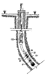
FIG. 9 shows a drilling tool (92) disposed in a well (9) according to one
embodiment of
the invention. The drilling tool (92) has a transmitter antenna (93), a
bucking antenna (95), and a
receiver antenna (97). The bucking antenna (95) can be connected with an
inverse polarity to
either the transmitter antenna (93) or to the receiver antenna (97). The
transmitter electronic
circuitry (99) is connected to the transmitter antenna (93) to provide time-
varying electric
currents to induce time-varying magnetic fields. Power supply (103) feeds the
circuitry (99).
Receiver circuitry (101) is connected to the receiver antenna (97) to detect
and measure resulting
EM signals. The bucking antenna (95) may also be omitted in another embodiment
by using
antennas adapted for independent mutual balancing as shown in FIGS. 7a, 7b,
and 7c. However,
this may reduce effectiveness where one desires Mx, M, MZ to have a common
origin.
Those skilled in the art will appreciate that the antenna apparatus of the
invention are not
limited to use in any one particular type of measurement or exploration
operation and that they
may be disposed within a well bore on any type of support member, e.g., on
coiled tubing, drill
collars, or wireline tools.
Parameters for the independently mutually balanced antennas (77, 78) of the
invention
are now presented. Cancellation of the undesired mutual coupling results in
the following
relationship:
NeAe _ NRAR
(10)
LB LR
-12-
CA 02447468 2003-10-29
where the subscripts B and R represent the mutual balancing coil and the
receiver coil,
respectively, and N is the number of turns, A is the effective area of the
coil, and L is the
distance from the transmitter coil.
Solving Equation 10 for AB gives the expression:
3
AB = NR LB AR . (11)
NB LR
Translation of the transverse coil for a small OLh is problematic, therefore a
comparable AAB is
added. To this end, the following relationship of a physical derivative is
considered:
AAB = dLB OLB (12)
e
For this statement to be true, the loop of area AAB should have an inductance
much
greater than its DC resistance. This is generally true because the resistance
of a loop is typically
in the sub-milli-ohm range. The inductance of a small circular loop of wire
is:
L0 =,u(2r-a 1- ~ K(k)-E(k) , (13)
where a is the conductor radius, r is the loop radius, K(k)and E(k)are
elliptic
integrals, and
kz = 4r(r - a) (14)
(2r - a)z
Put another way, this loop should generate a small opposing complex voltage in
the
receiver/bucking coil circuit. Equation 12 can be rewritten as
z
AAB = 3AROL NR LB
~ 3 . (15)
NB LR
The bucking loop radius can thus be shown to be
y
~B or r = 3ABOLB . (16)
~c KLB
-13-
CA 02447468 2003-10-29
FIG. 10 shows an arrangement for a transmitter or receiver antenna according
to an
embodiment of the invention. This arrangement consists of a transverse EM
antenna pair (105)
(similar to FIG. 4) combined with a solenoid coil (107) oriented so that its
dipole moment is
parallel to the longitudinal axis of the instrument (represented by the z-
axis). The solenoid coil
(107) is surrounded by coils (109) that have their magnetic moments
perpendicular to the
solenoid's magnetic moment.
Other embodiments of the invention may be implemented by "printing" the
conductive
coil(s) or elements directly onto the non-conductive core material through
plating or other
conventional deposition processes. One such embodiment comprises plating the
entire outer
diameter of the core with a conductive material and etching away the excess to
form the coil.
Another embodiment entails selectively plating only the shape of the coil onto
the core through
the use of masking techniques known in the art. Additional embodiments may
also be
implemented using other thin film growth techniques known in the art, such as
spray coating and
liquid phase epitaxy.
Several processes are known to entirely or selectively coat a dielectric
material with a
conductive material such as copper. These include, but are not limited to,
electroless plating and
the various vapor deposition processes. These techniques allow one to produce
a copper (or
other conductive material) overlay in the shape of a saddle coil onto a
ceramic or other dielectric
material core.
Electroless plating is one technique that may be used to implement the
invention. This
plating process enables the metal coating of non-conductive materials, such as
plastics, glasses
and ceramics. Compared to electroplating, the coatings derived from
electroless plating are
usually more uniform. The deposition is carried out in liquids (solutions),
and is based on
chemical reactions (mainly reductions), without an external source of electric
current.
Electroless plating is further described in GLENN O. MALLORY & JUAN B. HAJDU,
ELECTROLESS
PLATING (William Andrew Publishing, ISBN 0-8155-1277-7) (1990).
Other embodiments of the invention may be implemented using known thin film
deposition techniques. Deposition is the transformation of vapors into solids,
frequently used to
grow solid thin film and powder materials. Deposition techniques are further
described in
-14-
CA 02447468 2003-10-29
KRISHNA SESHAN, HANDBOOK OF THIN FILM DEPOSITION PROCESSES AND TECHNIQUES,
(William
Andrew Publishing, ISBN 0-8155-1442-5) (2001).
FIG. 12A shows an embodiment of the invention derived using a thin film
technique as
described above. As described above, the core (39) may be formed of any
suitable dielectric
material. It will be appreciated that practically any desired coil patterns
may be derived using
these techniques, including the mutual balancing configurations disclosed
herein. Conductive
disks (see item 72 in FIG. 7C) may also be added to the core (39) using these
techniques.
Connection points are shown at (40) for coupling the conductors to independent
circuitry. FIG.
12B shows an exploded view of the indicated antenna section of FIG. 12A,
illustrating the
conductor disposed on the core (39) surface. In this embodiment the non-coated
core (39') has
been masked during plating. Alternatively, the plating may also be removed
from this area to
form the desired pattern. FIG. 12C shows a cross-sectional view of the antenna
(74) taken along
a section of FIG. 12B. The conductive material is disposed on the outer
surface of the core (39)
to form the coil (23).
Advantages of these printed coil embodiments include a more robust joint
between the
conductor and the dielectric core, which may be stronger than either material
alone. Thus
providing an antenna that can withstand the stresses and strains encountered
in the downhole
environment, particularly in while-drilling applications. The core is also
easier to produce since
it is basically featureless.
While the antennas disclosed herein are generally shown as a one-piece annular
surface
of revolution, other embodiments of the invention may be implemented with the
core formed in
individual segments having individual conductive elements disposed thereon by
any of the
disclosed techniques. FIG. 13 shows such an embodiment. The core (39) provides
a base
forming a surface covering a ninety-degree sector. An independent saddle coil
(23) is disposed
thereon. Although the antenna (74) of FIG. 13 has an arcuate shaped core (39),
it may be formed
in practically any desired shape.
Another embodiment of the invention may include a semi-curved or flat core
(39), which
can be disposed within a pocket or recess (120) formed in the logging/drilling
tool (80, 90) as
shown in FIG. 14. Feed thru wires (130/132) are run along the recess to
connect to the coil (23)
on the core (39) surface. The wires (130/132) couple the coil (23) to
conventional electronics
-I5-
CA 02447468 2003-10-29
(not shown) adapted to energize the antenna with alternating current to
transmit electromagnetic
energy or to receive signals responsive to the receipt of electromagnetic
energy as known in the
art. A rubber overmold may also be disposed over the core (39) segment to
completely
encompasses the antenna (74) (not shown). A shield (not shown) may also be
placed over the
antenna (74) to protect the coil or provide electromagnetic energy focusing as
known in the art.
One or more of these independent antennas 74 could be placed on a downhole
tool to provide a
transverse magnetic dipole where desired with relative ease and repairs or
replacement could be
done in the field, reducing cost and delay.
FIG. 15 illustrates a process for producing an antenna of the invention. An
electrical
conductor is disposed on a dielectric core at step (200). The conductor forms
a conductive path
arranged to have a first magnetic dipole moment substantially perpendicular to
a longitudinal
axis of the core. At step (205), the electrical conductor is adapted to be
coupled with
independent circuitry as known in the art.
While the invention has been described with respect to a limited number of
embodiments,
those skilled in the art will appreciate that other embodiments can be devised
which do not
depart from the scope of the invention as disclosed herein. For example, the
antennas of the
invention may be configured using a combination of printed and wired coils.
Multiple overlaid
substrates may also be used to achieve modified couplings or to alter the
magnetic moment(s) as
desired. Using multiple-layered substrates would allow for antennas to be
collocated on the
support, e.g., a bucking and a receiver antenna. It will also be appreciated
that the embodiments
of the invention are not limited to any particular material for their
construction. Any suitable
material or compounds (presently known or developed in the future) may be used
to form the
embodiments of the invention provided they allow for operation as described
herein.
-16-