Note: Descriptions are shown in the official language in which they were submitted.
CA 02447722 2003-11-18
WO 02/095835 PCT/US02/14848
VERTICAL METAL OXIDE SILICON FIELD EFFECT
SEMICONDUCTOR DIODES
BACKGROUND OF THE INVENTION
1. Field of the Invention
The present invention generally relates to semiconductor
devices and fabrication of the same. The present invention
more particularly relates to semiconductor diodes and their
methods of fabrication.
2. Background Information
Semiconductor devices of various kinds are well known in
the prior art. Because the present invention relates to
semiconductor diodes and how they are fabricated, the focus
of this section will be semiconductor diodes.
Semiconductor diodes are widely used in electronic
circuits for various purposes. The primary purpose of such
semiconductor diodes is to provide conduction of current in a
forward direction in response to a forward voltage bias, and
to block conduction of current in the reverse direction in
response to a reverse voltage bias. This rectifying function
is widely used in such circuits as power supplies of various
kinds as well as in many other electronic circuits.
In typical semiconductor diodes, conduction in the
forward direction is limited to leakage current values until
the forward voltage bias reaches a characteristic value for
the particular type of semiconductor device. By way of
example, silicon pn junction diodes don't conduct
significantly until the forward bias voltage is at least
approximately 0.7 volts. Many silicon Schottky diodes,
because of the characteristics of the Schottky barrier, can
begin to conduct at lower voltages, such as 0.4 volts.
1
CA 02447722 2003-11-18
WO 02/095835 PCT/US02/14848
Germanium pn junction diodes have a forward conduction
voltage drop of approximately 0.3 volts at room temperature.
However, the same are currently only rarely used, not only
because of their incompatibility with silicon integrated
circuit fabrication, but also even as a discrete device
because of temperature sensitivity and other undesirable
characteristics thereof.
I
In some applications, diodes are used not for their
rectifying characteristics, but rather to be always forward
biased so as to provide their characteristic forward
conduction voltage drop. For instance, in integrated
circuits, diodes or diode connected transistors are
frequently used to provide a forward conduction voltage drop
substantially equal to the base-emitter voltage of another
transistor in the circuit. While certain embodiments of the
present invention may find use in circuits of this general
kind, such use is not a primary objective thereof.
In circuits which utilize the true rectifying
characteristics of semiconductor diodes, the forward
conduction voltage drop of the diode is usually a substantial
disadvantage. By way of specific example, in a DC to DC
step-down converter, a transformer is typically used wherein
a semiconductor switch controlled by an appropriate
controller is used to periodically connect and disconnect the
primary of the transformer with a DC power source. The
secondary voltage is connected to a converter output, either
through a diode for its rectifying characteristics, or
through another semiconductor switch. The controller varies
either the duty cycle or the frequency of the primary
connection to the power source as required to maintain the
desired output voltage. If a semiconductor switch is used to "
2
CA 02447722 2003-11-18
WO 02/095835 PCT/US02/14848
connect the secondary to the output, the operation of this
second switch is also controlled by the controller.
Use of a semiconductor switch to couple the secondary to
the output has the advantage of a very low forward conduction
voltage drop, though has the disadvantage of requiring
careful control throughout the operating temperature range of
the converter to maintain the efficiency of the energy
transfer from primary to secondary, The use of a
semiconductor diode for this purpose has the advantage of
eliminating the need for control of a secondary switch, but
has the disadvantage of imposing the forward conduction
voltage drop of the semiconductor diode on the secondary
circuit. This has at least two very substantial
disadvantages. First, the forward conduction voltage drop of
the semiconductor diode device can substantially reduce the
efficiency of the converter. For instance, newer integrated
circuits commonly used in computer systems are designed to
operate using lower power supply voltages, such as 3.3 volts,
3 volts and 2.7 volts. In the case of a 3 volt power supply,
the imposition of a 0.7 volt series voltage drop means that
the converter is in effect operating into a 3.7 volt load,
thereby limiting the efficiency of the converter to 81%, even
before other circuit losses are considered.
Second, the efficiency loss described above represents a
power loss in the diode, resulting in the heating thereof.
This limits the power conversion capability of an integrated
circuit converter, and in many applications requires the use
of a discrete diode of adequate size, increasing the overall
circuit size and cost.
Another commonly used circuit for AC to DC conversion is
the full wave bridge rectifier usually coupled to the
secondary winding of a transformer having the primary thereof
3
CA 02447722 2003-11-18
WO 02/095835 PCT/US02/14848
driven by the AC power source. Here two diode voltage drops
are imposed on the peak DC output, making the circuit
particularly inefficient using conventional diodes, and
increasing the heat generation of the circuit requiring
dissipation through large discrete devices, heat dissipating
structures, etc. depending on the DC power to be provided.
Therefore, it would be highly advantageous to have a
semiconductor diode having a low forward conduction voltage
drop for use as a rectifying element in circuits wherein the
diode will be subjected to both forward and reverse bias
voltages from time to time. While such a diode may find many
applications in discrete form, it would be further desirable
for such a diode to be compatible with integrated circuit
fabrication techniques so that the same could be realized in
integrated circuit form as part of a much larger integrated
circuit. Further, while reverse current leakage is always
undesirable and normally must be made up by additional
forward conduction current, thereby decreasing circuit
efficiency, reverse current leakage can have other and more
substantial deleterious affects on some circuits.
Accordingly it would also be desirable for such a
semiconductor diode to further have a low reverse bias
leakage current.
In many applications it is required that the diode be
' put across a coil such as a transformer. In these instances
it is possible for a reverse voltage to be applied to the
diode which will force it into reverse breakdown,
specifically into a junction avalanche condition. This is
particularly true in DC to DC converters which use a rapidly
changing waveform to drive transformer coils which are
connected across diode bridges. In these applications a
specification requirement for "Avalanche Energy" capability
4
CA 02447722 2003-11-18
WO 02/095835 PCT/US02/14848
is a parameter normally included in the data sheets. The
avalanche energy capability of a diode is a significant
factor for a designer of such circuits. The avalanche energy
capability determines how much. design margin a designer has
when designing a semiconductor diode into a circuit. The
larger the number of avalanche energy capability the more
design flexibility a circuit designer has.
The avalanche energy capability is a measure of the
diode's capability to absorb the energy from the coil, where
energy E = (1/2)*I2*L, without destroying the diode. These
requirements are typically on the order of tens of
millijoules. A key factor in the ability of a diode to
nondestructively dissipate this energy is the amount of
junction area which dissipates the energy i.e., the area of
the junction which actually conducts during avalanche. High
avalanche energy capability of a semiconductor diode improves
its utilization.
At the same time, it is desirable to lower the cost of
semiconductor diodes by reducing their size and by improving
their methods of fabrication.
BRIEF SUMMARY OF THE INVENTION
The present invention includes methods and apparatus as
described in the claims. Briefly, semiconductor diodes
having a low forward conduction voltage drop, a low reverse
leakage current, a high voltage capability and avalanche
energy capability, suitable for use in integrated circuits as
well as for discrete devices are disclosed. The
semiconductor diodes are diode configured vertical
cylindrical metal oxide semiconductor field effect devices
having one diode terminal as the common connection between
the gates and drains of the vertical cylindrical metal oxide
CA 02447722 2003-11-18
WO 02/095835 PCT/US02/14848
semiconductor field effect devices, and one diode terminal as
the common connection with the sources of the vertical
cylindrical metal oxide semiconductor field effect devices.
The method of manufacturing the vertical cylindrical metal
oxide semiconductor field effect devices is disclosed.
Various device terminations can be employed to complete the
diode devices. Various embodiments are disclosed.
Other aspects and features of the present invention will
become apparent to those ordinarily skilled in the art upon
review of the following description of specific embodiments
of the invention in conjunction with the accompanying claims
and figures.
BRIEF DESCRIPTION OF THE DRAWINGS
The features and advantages of the present invention
will become apparent from the following detailed description
of the present invention in which:
Figure 1 is a circuit diagram for a well known AC to DC
converter using a full wave bridge rectifier in which the
present invention may be used.
Figures 2A-2B are schematic diagrams of n-channel and p-
channel metal oxide semiconductor field effect devices which
are diode connected in accordance with the present invention.
Figure 2C is a schematic diagram of the equivalent
circuit of the diode connected metal oxide semiconductor
field effect devices of Figures 2A and 2B.
Figures 3A-3N are cross-sectional views illustrating
steps in an exemplary process for fabricating the diode
connected vertical metal oxide semiconductor field effect
devices of the present invention.
6
CA 02447722 2003-11-18
WO 02/095835 PCT/US02/14848
Figures 4A-4N are cross-sectional views illustrating
steps in another exemplary process for fabricating the diode
connected vertical metal oxide semiconductor field effect
devices of the present invention.
Figures 5A-5C are top views of exemplary alternate
structures for the vertical MOSFED diode of the present
invention.
Figure 6 illustrates active diode areas on a wafer on
which a plurality of vertical MOSFED diodes are formed.
Figure 7 is a schematic diagram of the electrical
equivalent of one active diode area.
Like reference numbers and designations in the drawings
indicate like elements providing similar functionality.
DETAILED DESCRIPTION OF THE PRESENT INVENTION
First referring to Figure 1, a circuit diagram for a
well known AC to DC converter using a full wave bridge
rectifier in which the present invention may be used may be
seen. In such circuits, a transformer 110 is used to provide
DC isolation between the primary and secondary circuits and
frequently to provide an AC voltage step-up or step-down to
the full wave bridge, comprised of diodes D1, D2, D3 and D4.
When the secondary lead 112 is sufficiently positive with
respect to secondary lead 114, diode D2 will conduct through
resister 116 to charge or further charge capacitor 118 and to
provide current to load 119, which current returns to lead
114 of the transformer through diode D3. Similarly, during
the other half cycle of the AC input voltage, when the
voltage on secondary lead 114 is sufficiently positive with
respect to secondary lead 112, diode D4 will conduct to
provide current through. resistor 116 to charge capacitor 118
7
CA 02447722 2003-11-18
WO 02/095835 PCT/US02/14848
and to provide current to load 119, with the capacitor and
load currents being returned to the secondary lead 112
through diode D1. Thus it may be seen that each time current
is delivered from the full wave bridge of diodes D1 through
D4 to the output of the bridge, two diode voltage drops are
imposed in series with that output. Further, since any pair
of diodes conduct only when the voltage across the secondary
of the transformer 110 exceeds the voltage across capacitor
118 by two diode voltage drops, it is clear that current is
delivered to the output of the bridge only during a fraction
of the time, namely when the transformer secondary voltage is
at or near a positive or negative peak.
The circuit of Figure 1 is merely exemplary of the type
of circuit in which the present invention is intended to be
used. These circuits may be characterized as circuits
wherein the diode will be subjected to both positive
(forward) and negative (reverse) differential voltages across
the two diode connections and the function of the diode is a
rectifying function to provide a DC or rectified current
output. This is to be distinguished from applications
wherein the desired function of a diode is to provide a
voltage reference responsive to the forward conduction
voltage drop characteristic of the diode when conducting
current, whether or not the diode will be subjected to
negative differential voltages also when in use. The
circuits in which the present invention is particularly
suited for use may also be characterized a's circuits wherein
the diode or diodes will be subjected to both positive and
negative differential voltages across the diode connections
and the function of the diode or diodes is a power rectifying
function to provide a DC or rectified current output of
sufficient power level to power one or more circuits
connected thereto. This is to be distinguished from
8
CA 02447722 2003-11-18
WO 02/095835 PCT/US02/14848
applications wherein the desired function of the diode is to
provide a signal-level current output which is used or
processed in a subsequent circuit not powered by the DC or
rectified current output of the diodes.
In many circuits of the type shown in Figure 1, a linear
voltage regulator may be used in the output in addition to
smoothing capacitor 118. Further, resistor 116, which serves
as a current limiting resistor, may be eliminated as a
separate circuit component in favor of the secondary
resistance of the transformer, as the transformer, in
substantially all applications of interest, will be an actual
discrete component of sufficient size to dissipate the power
loss therein. Of particular importance to the present
invention, however, are the diodes D1 through D4 themselves,
as the power loss in these diodes in general serves no
desired circuit function, but rather merely creates unwanted
power dissipation and heat, requiring the use of larger
diodes, whether in discrete form or integrated circuit form,
and actually increases the size of the transformer required
to provide this extra power output, e.g., the power required
by the load plus the power dissipated by the diodes.
The present invention is directed to the realization of
diodes and/or diode functions having low diode forward
conduction voltage drops, low reverse current leakage, and
high voltage capabilities for use primarily in such circuits
and other circuits wherein the diodes may be or are in fact
subjected to forward and reverse bias in use. This is
achieved in the present invention through the use of diode
connected field effect devices, shown schematically in
Figures 2A and 2B as n-channel and p-channel diode connected
field effect devices, respectively. In accordance with the
preferred embodiment of the invention, such devices are
9
CA 02447722 2003-11-18
WO 02/095835 PCT/US02/14848
fabricated through the use of common gate and drain
connections, typically a common conducting layer on the
substrate, and more preferably through one or more special
fabrication techniques which enhance the electrical
characteristic of the resulting device. Figure 2C
illustrates the equivalent diode of the diode connected field
effect devices of Figures 2A and 2B with the respective anode
"A" and cathode "C" terminals.
The present invention implements a semiconductor diode
by forming one or more vertical and cylindrical shaped metal
oxide semiconductor field effect transistor (MOSFET) having a
diode connected configuration. One or more parallel
connected vertical and cylindrical shaped metal oxide
semiconductor field effect transistors (MOSFET) having a
diode connected configuration are referred to as a diode
configured vertical metal oxide semiconductor field effect
device or devices (MOSFED).
In manufacturing the diode configured vertical MOSFED,
the masking arid manufacturing techniques described in United
States Patent Application No. 09/689,074 entitled "METHOD AND
APPARATUS FOR PATTERNING FINE DIMENSIONS" filed by Richard A.
Met~ler on October 12, 2000 which is incorporated herein by
reference can also be used to reduce the cost of masking and
provide finer lines in the present invention than might
otherwise be available.
Processes for fabricating embodiments of the present
invention are presented herein in relation to the cross-
sectional views of Figures 3A-3N and Figures 4A-4N. These
exemplary processes form the diode configured vertical metal
oxide semiconductor field effect devices (MOSFED) of the
present invention. An individual diode configured vertical
metal oxide semiconductor field effect device can be
CA 02447722 2003-11-18
WO 02/095835 PCT/US02/14848
essentially thought of as a cylindrical and vertical metal
oxide semiconductor field effect transistor connected with a
common gate-drain connection. (In that regard, for purposes
of specificity herein, the source and drain are identified in
the normal forward conduction sense, it being recognized that
the source and drain reverse in the case of a reverse biased
device.) The diode configured vertical metal oxide
semiconductor field effect devices of the present invention
may also be referred to as vertical MOSFED diodes. However,
the present invention is not a traditional metal oxide
semiconductor field effect transistor (MOSFET) because it
operates differently and is formed by a different process.
As shall be subsequently seen, in a typical application a
large plurality of tightly packed MOSFED devices are formed
on a single substrate, all having a common gate-drain
connection and a common source connection. Consequently,
MOSFED as used herein may refer to a single device of
multiple commonly connected devices on a single substrate.
Referring now to Figures 3A-3N, cross-sectional views
illustrating steps of an exemplary process for fabricating
the diode connected vertical metal oxide semiconductor field
effect devices of the present invention are illustrated. The
diode connected or diode configured vertical MOSFEDs are
formed using cylindrical pedestals. Figures 3A-3L show only
a portion of a wafer illustrating the formation of a single
MOSFED device. Typically, such multiple devices are
simultaneously formed by replicating clusters of large
numbers of commonly connected devices across larger portions
or an entire semiconductor wafer. Also typically each
cluster of multiple devices with incorporate some form of
edge termination as is well known in the prior art to provide
the breakdown voltage as needed.
11
CA 02447722 2003-11-18
WO 02/095835 PCT/US02/14848
Figure 3A shows a starting silicon substrate,300 of a
wafer having two silicon epitaxial layers thereon. The first
silicon epitaxial layer 301, directly on top of the substrate
300, is of the same conductivity type as the substrate, and
is provided in order to form an increased reverse bias
breakdown voltage for diode devices. The second epitaxial
layer 302, directly on top of the first layer, and forming
the surface of the wafer, is of the opposite conductivity
type. In one embodiment with an N-type substrate, the first
silicon epitaxial layer has a resistivity of approximately
1.1 ohm-crn and a thickness of approximately 3~,m in order to
achieve a reverse bias breakdown voltage of about forty-five
volts. The second P-type epitaxial layer has a resistivity
of 0.2.5 ohm-cm, 0.6 um thick which is selected to determine
the MGSF'ED threshold. Epitaxial wafers having the siJ_icon
epitaxial layers can be purchased as starting material, or
formed as part of the processing of the diode using well
known standard epitaxial growth tecr~niques. The second
epitaxial layer can be replaced by deposition or impl«nt
techniques followed by a drive thereby forming the second
conductivity type in the surface of the first epitaxial
layer.
Tn th.e case of an N-type silicon substrate, the lower or
backside surface of the substrate 300 may form tyke cathode
while a portion of the top surface of the substrate 300 is
formed to be the anode. In the case of a P-type silicon
substrat;F, the diode terminals are reversed and the lo~,aer or
backs i de swrf.ace of t.ie substrate 300 may form the anode
while a portion of the top surface of the substrate 300 is
formed to be the cathode.
A thin oxide layer 3U3 is grown on the surface of the
substrate 3U0 as shown in Figure 3B to randomize the sheet
12
CA 02447722 2003-11-18
WO 02/095835 PCT/US02/14848
implant which is to follow. The thin oxide 303 is typically
three hundred Angstroms (300A) in thickness. The sheet
implant that follows requires no masking by a mask, but
rather is composed of ions that are implanted over the entire
wafer. The sheet implant is to provide a good ohmic contact
for the P-type back gate region of the vertical MOSFED diode.
The implant is a Boron implant at about 4x10¹⁵ atoms per cm~
with an energy of 15 KeV.
Referring again to Figure 3B, completion of a first
masking step is illustrated. Prior to the first masking step
and etching, a layer of oxide is applied on top of the thin
oxide 303 across the wafer. The oxide layer is then
patterned using a mask and areas are etched away, including
parts of the thin oxide 303 to form cylindrical shaped
construction pedestals 304 on top of the thin oxide 303. The
cylindrical shaped construction pedestals 304 are
approximately 1.0 microns (gym) high in one embodiment. The
shape of the pedestals 304 can be any cylindrical shape,
including but not limited to, circular, hexagonal, square,
rectangular, as well as other solid shapes such as
serpentine, etc. For ease of~description herein, the
cylindrical shape will be presumptively rectangular forming
rectangular cylindrical pedestals or bars formed out of the
oxide layer. Figure 3B illustrates a cross-section of four
of a plurality of rectangular cylindrical pedestals 304 that
are formed across the silicon wafer. The dimensions of the
rectangular cylindrical construction pedestals 304 in one
embodiment are approximately 0.15 microns in width,
approximately 1.0 micron in height, with a pitch of
approximately 0.4 microns. It is understood that these
dimensions can be altered in coordination with any adjustment
in the implantation levels in order to provide similar device
physics for a diode configured vertical MOSFED. Region 310
13
CA 02447722 2003-11-18
WO 02/095835 PCT/US02/14848
of silicon wafer is exploded into Figure 3C in order to
further detail the processing around each of the plurality of
pedestals 304.
Referring now to Figure 3C, the exploded view of region
310 of Figure 3B is illustrated. The rectangular cylindrical
construction pedestal 304 is formed on the surface of the
thin oxide 303 on the substrate 300. Figures 3D-3L
illustrate the further processing of the diode configured
vertical MOSFED with respect to the rectangular cylindrical
construction pedestal 304 of Figure 3C.
Referring now to Figure 3D, the thin oxide layer 303 and
a portion of the substrate 300 between pedestals 304 have
been etched away to a depth of about 500A, forming shallow
silicon trenches 308 and substrate pedestals 309. This etch
step is a Reactive Ion Etch (RIE, a directional etch)
commonly used in silicon. processing to form trench. metal-
oxide-semiconductor (MOS) transistors and capacitors. An N-
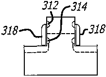
type anode contact implant is now performed, typically
Arsenic, with a dose of 3E15 and energy of l5KeV. This
provides regions 312 around the periphery of each pedestal
that will become the anode region (drain) at the surface of
the device.
Referring now to Figure 3E, additional silicon etching
has been performed to a depth of 0.6um. This leaves an anode
region 312 at the top of the silicon pedestal structure.
This is followed by another Arsenic implant 314, with a dose
of 3e14 at l5KeV, to form the source of the FED.
The result of a third silicon etch for another 500 A is
presented in Figure 3F. This removes the major portion of
the second implant in the bottom of the trench, leaving an
isolated source implant 314 in contact with the N-type
14
CA 02447722 2003-11-18
WO 02/095835 PCT/US02/14848
epitaxial layer if used, or to the N-type substrate if an N-
type epitaxial layer is not used. This second implant is not
necessary, and an alternate embodiment builds the device
without this second implant and third silicon etch. This
second implant may be useful however to lower the on
resistance of the devices.
As presented in Figure 3G, the remaining part of the
oxide pedestal is stripped away, and a layer of gate oxide
316, 100.A thick, and a layer of heavily doped poly silicon
318 are conformally deposited on the device in the first
stage of the gate formation.
The next process is the RIE etching (a directional etch)
of the poly silicon layer, stopping on the oxide layer, to
form a side wall gate regions 318 shown in Figure 3H. This
is followed by a Boron implant that forms a P-type region 320
to block the potential from the bottom of the gate oxide
during reverse bias (off).
A further poly silicon RIE etch is performed as shown in
Figure 3I. This moves the top of the poly gates 318 down to
allow access to the drain elements. Following this is an
oxide etch to remove the gate oxide as shown in Figure 3J.
This prepares the surfaces for the application of a metal
diffusion barrier 322 such as TiSi or TiW. Figure 3K shows
the finished device with a barrier metal layer 322, and a top
metal layer 324 applied over the structure.
Figure 3L presents a finished section of four pedestals
with the final metal applied. Not shown however is the
source contact for the device. In some applications, the
source contact is made by depositing a metallization layer
330 on the back of the substrate 300 opposite the vertical
MOSFED devices 332, as shown in Figure 3M. In other
CA 02447722 2003-11-18
WO 02/095835 PCT/US02/14848
applications, the vertical MOSFED devices 332 are formed in a
well 334, and the source contact is made by depositing a
metallization layer 330 on the well surface adjacent or
surrounding°the vertical MOSFED devices, as shown in Figure
3N,
Now referring to Figures 4A through 4M, an alternate
process for forming the MOSFEDs of the present invention may
be seen. In this process, the initial steps are the same as
for that described with respect to Figure 3, specifically
Figures 3A through 3D. Accordingly, Figures 4A through 4D
are identical to Figures 3A through 3D and use the same
numerical identifications. Following the n-type anode-
contact implant forming regions 312 of Figure 4D, an oxide
layer is deposited and then etched back using a directional
etch to leave sidewall regions 400 as shown in Figure 4E.
Thereafter, a further directional etch step is performed
(Figure 4F), followed by a further n-type, typically arsenic,
implant forming n-type regions 402. A further directional
etch step is then performed, leaving source regions 402 as
shown in Figure 4G. Thereafter, the oxide sidewall regions
400 are stripped away, as shown in Figure 4H, providing
greater physical access to regions 312 than in the previous
embodiment. The remaining part of the oxide pedestals is
also stripped away.
The next step is to put down a layer of gate oxide 404
and a layer of heavily doped polysilicon 406, as shown in
Figure 3I. A directional etch then removes the polysilicon
from the horizontal surfaces of the oxide layer 404, leaving
sidewall portions 406 as shown in Figure 4J. Further
directional etching reduces the height of the sidewall
regions 406, specifically to remove the polysilicon from
regions 408. Thereafter, removing the gate oxide layer from
16
CA 02447722 2003-11-18
WO 02/095835 PCT/US02/14848
the exposed surfaces exposes regions 312, after which a
diffusion barrier 410 and a top metal layer 412 are deposited
to form the final structure.of Figure 4M for a single
cylindrical device, or of Figure 4N for multiple devices. As
before, the source contact may be made by a metallization
layer on the opposite side of the substrate, such as
metallization layer 330 of Figure 3M, or alternatively, by a
metallization layer contacting a well in which the
cylindrical, devices are formed as in Figure 3M.
Referring now to Figures 5A-5C, top views of exemplary
arrays of diode configured vertical MOSFEDs are illustrated.
In Figure 5A, the diode configured vertical MOSFEDs 340 are
formed using circular cylindrical pedestals. In Figure 5B,
the diode configured vertical MOSFEDs 340 are formed using
rectangular of square cylindrical pedestals. In Figure 5C,
the diode configured vertical MOSFEDs 340 are formed using
hexagonal cylindrical pedestals. Other cylindrical shapes
can be used for the pedestals in order to form different
shapes of the diode configured vertical MOSFEDs 340.
Referring now to Figure 6, a plurality of diode active
areas 90 are separated by scribe channels 91 between the
diode active areas 90 on the wafer. In each diode active
area 90 are a plurality of diode configured vertical MOSFEDs
340. Edge termination of the diode active areas in the
scribe channels 91 can be provided through several
semiconductor device terminations including the tapered
termination of U.S. Patent No. 5,825,079 entitled
"Semiconductor diodes having low forward conduction voltage
drop and low reverse current leakage" filed by Richard A.
Metzler and Vladimir Rodov on January 23, 1997 or the mesa
termination described in U.S. Patent Application No,
09/395,722 entitled "Method and Apparatus for Termination of
17
CA 02447722 2003-11-18
WO 02/095835 PCT/US02/14848
Semiconductor Devices" filed by Richard Metzler on September
14, 1999. Additionally, well known single or multiple normal
ring terminations can be used or, voltage permitting, a
simple guard ring integral with the device active diffusions
can be used.
Referring now to Figure 7, the schematic equivalent of
the diode active area having multiple diodes 340 connected in
parallel, each representing a diode configured vertical
MOSFED. Adding the current capability of each of the diode
connected vertical MOSFED devices 340 results in a large
current carrying capability. It is understood that there may
be several hundred or more MOSFED device active areas 90 in
each cluster on a wafer, with only four being shown in Figure
9. Each individual diode active area 90 can contain
thousands of individual diode configured vertical MOSFEDs
340.
With respect to the current capability of the diode, the
forward current is a function of the number of diode
configured vertical MOSFEDs 340 which are coupled in parallel
together.
With respect to the threshold voltage, by appropriately
selecting the dopant.s, their concentrations, and other
materials and dimensions for fabrication of the diode
configured vertical MOSFED, the channel regions may be made
to just conduct at substantially zero forward bias across the
anode and cathode. Thus, in true rectifying applications
such as in power supplies and the like, the present invention
results in reduced power consumption and heating in the
rectifying devices, and greater overall efficiency of the
resulting circuits.
18
CA 02447722 2003-11-18
WO 02/095835 PCT/US02/14848
There has been disclosed herein certain exemplary
methods of fabricating diode configured vertical MOSFEDs, as
well as the MOSFEDs so made. It will be noted that in the
exemplary processes there is a single masking step having
only a trivial alignment requirement with respect to the
semiconductor substrate on which the MOSFEDs are to be
formed. Thereafter, each additional step is self-aligning
with respect to the prior step, thereby eliminating multiple
masks, and particularly the critical alignment requirement
between individual masks of mask sets typically used for the
fabrication of semiconductor devices. This simplifies
processing, increases yields and reduces wafer to wafer
device variations due to differences in mask alignment.
In certain instances in the foregoing description,
certain alternate materials and methods were set forth. It
is to be noted however, that the identification of specific
alternative materials and processes is not to infer that
still other materials and processes for those or other steps
in the process of fabrication or in the resulting diode
devices are excluded from use in the present invention. To
the contrary, steps and materials other than those set out
herein will be obvious to those skilled in the art. Thus
while the present invention has been disclosed and described
with respect to certain preferred embodiments, it will be
understood to those skilled in the art that the present
invention diodes and methods of fabricating the same may be
varied without departing from the spirit and scope of the
invention.
19