Note: Descriptions are shown in the official language in which they were submitted.
CA 02447929 2003-11-21
WO 01/90730 PCT/CA01/00717
SCANNING KELVIN MICROPROBE SYSTEM.AND
PROCESS FOR ANALYZING A SURFACE
FIELD OF THE INVENTION
This invention relates to processes for measurement and analysis of surfaces
utilizing
Kelvin methodology, and more specifically to the development and use of an
improved
scanning Kelvin microprobe (SKM) for surface measurement and analysis.
BACKGROUND OF THE INVENTION
The Kelvin method for the measurement of work function can be employed for the
analysis of a wider range of materials, at different temperatures and
pressures, than any other
surface analysis technique. Work function is a very sensitive parameter which
can reflect
imperceptible structural variations, surface modification, contamination or
surface-related
processes. The method is now regaining popularityl'4 as a powerful technique
because of its
inherent high surface sensitivity, high lateral resolution due to the
availability of nanometric
precision-positioning systems, and improved signal detection devices. Unlike
many other
methods, the measurement of work function does not depend on an estimate of
the electron
reflection coefficient on the surface. Moreover, the technique does not use
high temperature,
high electric fields, or beams of electrons or photons. Being a non-contact
and non-
destructive method, it does not pose the risk of desorbing or removing even
weakly-bound
species from the surface. Furthermore, the Kelvin method is a direct
measurement method
requiring only a simple experimental set-up with no sample preparation.
When an electron is removed from a point witlun a material, the total change
of
thermodynamic free energy of the whole system is the difference between the
change of the
electrochemical potential of that material and the change of the electrostatic
potential of the
electron. If the electron is removed from a surface to a point in a vacuum,
far from the outside
surface so the stuface forces have no more influence on the electron, this
change of free
energy is called the work function of that surface. The corresponding change
when the
electron is removed to another material that is in intimate electrical contact
and thermal
equilibrium with the first material, is called the contact potential
difference (CPD). For
example, when two different conductors are first brought into electrical
contact, free electrons
flow out of the one with the higher electrochemical potential (i.e., Fermi
level) into the other
CA 02447929 2003-11-21
WO 01/90730 PCT/CA01/00717
2
conductor. This net flow of electrons continues until equilibrium is reached
when their
electrochemical potentials have become equal. The metal of higher world
function (having
originally a lower electrochemical potential) acquires a negative charge, the
other conductor
being left with a positive charge. When the whole system reaches thermodynamic
equilibrium, the resulting potential difference is the CPD and is equal to the
difference
between their worse functions.
In order to measure the CPD it is necessary to connect the conductors. A
direct
measurement with a voltmeter included in the circuit is not possible, since
the algebraic sum
of all the CPDs in the circuit is zero. Thus, CPD must be measured in an open
circuit i.e.,
using a dielectric such as a vacuum or air between the conductors.
The Kelvin method is based on a parallel plate capacitor model: a vibrating
electrode
suspended above and "parallel" to a stationary electrode. The sinusoidal
vibration changes the
capacity between plates, which in turn, gives a variation of charge generating
a displacement
current, the Kelvin current, proportional to the existing CPD between the
electrodes.
The last century witnessed a continuous process of improving and modification
of the
Kelvin probe in order to adapt it for particular applicationss-lo. The probe
has been used in
surface chemistry investigations, surface photo voltage studies, corrosion,
stress, adsorption
and contamination studies and was adapted for measurements in liquids, at high
temperatures,
in ion or electron emitting samples or in an ultra high vacuum environments-
ss. The problem
of conducting measurements at the micrometer and sub-micrometer level has been
overcome
with the advent of SKM format which offers a new and unique tool to image the
electrical
potential on surfaces at the micrometer and sub-micrometer level. It has also
been possible to
develop an SKM instrument that is capable of generating both CPD and surface
topographical images in tandems. Such equipment not only provides an
electrical image of a
surface, but also generates a truly tandem topographical image. Accordingly,
electrical
information can be integrated fully with chemical and morphological details,
an extremely
valuable feature for the users of the surface characterization technologies.
However, to measure the CPD on a small scale with high precision it is
necessary to
control closely the distance between the tip and the sample. This has been
initially aclueveds
by processing the harmonics of the Kelvin current. However, this approach
Ieads to
instability and is unreliable.
CA 02447929 2003-11-21
WO 01/90730 PCT/CA01/00717
SUMMARY OF THE INVENTION
It is an object of the present invention to obviate or mitigate at Ieast one
disadvantage
of prior art processes, systems and methods applying SKM for microanalysis of
surfaces.
The invention provides a scanning Kelvin microprobe system for analyzing a
surface
of a sample, the system comprising: a tip with a predetermined Worl~ function
for exploring a
surface of the sample, and for extracting Kelvin current from the local
capacitor formed
between the tip and the sample; a scan table for placing the sample thereon; a
micropositioner
for moving the scan table in x and y directions, a piezoelectric translation
stage attached to
the scan table for moving the sample in the z direction for maintaining a
constant sample-tip
distance; a charge aanplifier for converting the Kelvin current extracted by
the tip into a
voltage; a fixst lock-in amplifier tuned at a first frequency for measuring
the voltage and
generating a contact potential difference image signal; a second lock-in
amplifier tuned at a
second frequency for monitoring sample-tip distance and for generating a
topographic image
signal, the second frequency being above the first frequency; and a controller
for controlling
the micropositioner.
The invention further provides a process for analyzing a surface of a sample
using a
scanning Kelvin microprobe system, comprising the steps of: placing a sample
on a scan
table; exploring a surface of the sample with a tip having a predetermined
work function;
extracting Kelvin current from a local capacitor formed between the tip and
the sample;
amplifying the Kelvin current extracted by the tip; measuring the Kelvin
current and
generating a contact potential difference signal using a first lock-in
amplifier tuned at a first
frequency; and monitoring distance between the sample and the tip and
generating a
topographic image signal using a second loch-in amplifier tuned at a second
frequency, the
second frequency being above the first frequency.
The SKM system of the invention uses a higher frequency (sample-tip
capacitance
detection) to control the sample-tip distance, thus, malting the process
stable and reliable.
The automated monitoring of the contact potential and topography was achieved
using 2
loch-in amplifiers tuned respectively on the vibrational frequency and on the
capacitance-
detection frequency. This means that the monitoring of the sample-tip distance
is no longer
CA 02447929 2003-11-21
WO 01/90730 PCT/CA01/00717
4
achieved by processing the harmonics of the CPD signal as taught by the prior
art, but by
measuring the sample-tip capacitance at a frequency above the vibrational
frequency. This
approach solves the instability and unreliability problems that affect the
prior art. The current
prototype has a superior lateral resolution achieved by employing amplifiers
capable of
detecting low-level currents extracted by extremely fine tip probes having an
apex radius of
curvature below 100 nm. The invention advantageously comprises a data
acquisition and
imagining system. Further, the null-condition measurement according to the
invention avoids
the strong electric fields that affect the surface of the specimens in prior
art apparatuses. This
is also an advantage over the force microscopes operating in Kelvin mode that
develop
extremely high local electrical fields (109 V/m range), thus affecting both
the local
distribution of charges and the spatial conformation of the investigated
molecules.
The scanning instrument developed is capable of CPD measurement to a lateral
resolution of 1 micron and can display a resolution of 1 mV. The
instrumentation according
to the invention fulfils a long-standing need for high resolution
measurements. With this
instrument, it is now possible to generate new knowledge and applications in
surface physical
chemistry and material characterization. Advantageously, the technique is non-
destructive. It
can be used to examine a wide range of substrates whether they are conductors,
semiconductors or insulators. The invention has applications in many technical
fields such as
surface chemical analysis, photochemical studies, corrosion, stress,
triboelectricity, polymers
and ferroelectric materials, adsorption and contamination, nano-devices,
microelectronic
fabrication, biochemical microarrays and biosensor technology.
Other aspects and features of the present invention will become apparent to
those
ordinarily skilled in the art upon review of the following description of
specific embodiments
of the invention in conjunction with the accompanying figures.
BRIEF DESCRIPTION OF THE DRAWINGS
Embodiments of the present invention will now be described, by way of example
only, with reference to the attached Figures.
Figure 1 is a diagrammatic illustration of the measurement of contact
potential
difference CPD according to the invention.
CA 02447929 2003-11-21
WO 01/90730 PCT/CA01/00717
Figure 2 is a schematic drawing of the instrument used in exemplary
embodiments of
the invention described herein.
Figure 3 shows a flow chart of a software program developed to control an SKM
system according to an embodiment of the invention.
5 ~ Figure 4 is a CPD image of a silver surface.
Figure 5 is a CPD image of a silver surface after surface treatment.
Figure 6 is a CPD image of silver on a mica surface.
Figure 7 illustrates the topography of silver on a mica surface.
Figure 8 illustrates the topography of a graphite surface.
I O Figure 9 is a CPD image of a highly-ordered pyrolitic graphite surface.
Figures 10A and 1 OB are depictions of tandem measurements of topography and
CPD image, respectively, of patterned aluminum deposition on silicon wafer.
Figures 11A and 11B are depictions of tandem measurements of topography and
CPD image, respectively, of a bare silicon wafer as an oligonucleotide
substrate.
Figure 12 is a CPD image of an oligonucleotide (F1) attached to an Si surface
according to an embodiment of the invention.
Figure 13 is a CPD image of an FI:Fz duplex attached to an Si surface
according to an
embodiment of the invention.
Figure 14 depicts a topographical image of a rnicromachined structure
patterned by
laser micromachine technology on a TSM (Thicl~ness-Shear Mode) sensor with one
channel
of S ~.m width.
Figure 15 depicts a topographical image of micromachined structure patterned
by
laser micromachine technology on a TSM (Thickness-Shear Mode) sensor with five
chamzels
of 5 ~.m width.
Figure 16A and 16B represent the CPD images of silicon-based polymer obtained
from explanted breast implant that has been exposed to the inside surface,
closest to the chest
cavity (A), and to the biological tissue towards the outside (B).
DETAILED DESCRIPTION
The invention relates to a scanning Kelvin microprobe system for analyzing a
surface
of a sample. The system.comprises a tip with a predetermined work function for
exploring
CA 02447929 2003-11-21
WO 01/90730 PCT/CA01/00717
6
the surface of the sample. The tip extracts Kelvin current from the local
capacitor which is
formed between the tip and the sample. The sample is placed on a scan table,
and a
micropositioner is used to move the scan table in x and y directions, allowing
the tip to
explore the surface. A piezoelectric translation stage is attached to the scan
table, and is used
to move the sample upwardly or downwardly toward or away from the tip, so as
to maintain a
constant sample-tip distance. The system further comprises a charge amplifier
for converting
the Kelvin current extracted by the tip into a voltage. A first Iock-in
amplifier is provided,
which is tuned at a first frequency. The first lock-in amplifier measures the
voltage and
geneYates a contact potential difference image signal. A second lock-in
amplifier is also
provided, which is tuned at a second frequency. The second lock-in amplifier
monitors
sample-tip distance and generates a topographic image signal. The system also
comprises a
controller for controlling the micropositioner.
The invention also relates to a process for analyzing the surface of a sample
using a
scanning Kelvin microprobe system. The process involves placing a sample on a
scan table,
and exploring the surface of the sample with a tip having a predetermined work
function.
Kelvin current is extracted from a local capacitor formed between the tip and
the sample, and
the Kelvin current extracted by the tip is amplified. The amplified Kelvin
current is
measured and from this measurement, a contact potential difference signal is
generated using
a first lock-in amplifier tuned at a first frequency. The distance between the
sample and the
tip is monitored, a topographic image signal is generated using a second lock-
in amplifier
tuned at a second frequency. The second frequency is above the first
frequency. The steps of
the process may be controlled using a software program capable of opening a
file, initializing
a card and a motor, starting first and second lock-in amplifiers, bringing the
tip down,
scanning the sample, bringing the tip up, writing data in a file, and closing
the file.
The sample to be analyzed according to the invention can a conductor,
semiconductor,
insulator, chemical, biochemical, photochemical, a chemical sensor, a
biosensor, a
biochemical microarray, a microelectronic device, and electronic image device,
a
micromachine device, a nano-device, a corroded material, a stressed material,
a coating, an
adsorbed material, a contaminated material, an oxides, a thin film or a self
assembling
monolayer.
CA 02447929 2003-11-21
WO 01/90730 PCT/CA01/00717
The scan table is movable by aazy requisite amount so as to allow exploration
of a
sample surface, for example by about 200 mn in either the x or y direction.
The scan table
may optionally have course and fine adjustment, for example, coarse adjustment
of about 100
nm and fine adjustment of about 4 nm.
A data acquisition system may be incorporated into the scanning Kelvin
microprobe
system, for acquiring the contact potential difference image signal and said
topographical
image signal.
The controller comprises software capable of opening a file, initializing a
card and a
motor, starting the first and the second lock-in amplifiers, bringing the tip
down, scanning the
sample, bringing the tip up, writing data in a file, and closing the file.
Kelvin current is generated when two electrodes or plates are brought in
electrical
contact with a measuring device and the Fermi levels 'of two electrodes
equalize. The Kelvin
current is a measure of contact potential difference (CPD) of the two
electrodes.
Contact potential difference is the difference between the work functions of
two
materials in contact. Measurement of the CPD thus affords a method of
measuring work
function differences between materials. In order to measure the CPD it is
necessary to
connect the materials. A direct measur ement, for instance with a voltmeter,
requires a circuit
shortened by a measurement device. However, in a closed circuit CPD cannot be
measured
directly, as the sum of the three interfacial differences would be zero,
except for the case
where the interfaces have different temperatures. Thus, CPD is measured in an
open circuit,
for example using a dielectric medium such as a vacuum or air.
Work function is the work required to extract an electron from the Fermi level
to
infinity.
A local capacitor is formed between the tip and the sample. The tip extracts
Kelvin
current from this local capacitor. A capacitor is capable of storing charges,
formed by
arrangement of two conductors or semiconductors (electrodes or plates)
separated by a
dielectric medium, such as air or a vacuum.
Capacitance is the property of a material whereby it stores elecfiric charge.
If an
isolated conductor is placed near a second conductor or a semiconductor but is
separated
from it by air or some other insulator, the system forms a capacitor. An
electric field is
CA 02447929 2003-11-21
WO 01/90730 PCT/CA01/00717
produced across the system and this field determines the potential difference
between the two
plates of the capacitor. The value of the capacitance of a given device is
directly proportional
to the size and shape (area) of the electrodes and the relative permittivity
of the dielectric
medium, and inversely proportional to the distance between the two plates.
According to the
invention, the tip and the sample act as the two plates of the capacitor, and
air is the dielectric
medium
The tip of the scanning Kelvin microprobe system according to the invention is
used
to scan a sample and to extract Kelvin current from the capacitor formed
between the tip and
the sample. The tip can be made of any suitable material with a known work
function, for
example, tungsten. In one embodiment of the present invention, the tip is a
guarded
microelectrode having the apex radius of curvature less than about 100 mn, and
optionally in
the range of about 50 nm.
The sample is placed on a scan table, which is capable of moving in the x, y,
and z
directions. The micropositioner provides a means for moving the scan table in
x and y
directions, and expediently comprises a computer-related device. A translation
stage is used
to move the scan table in z direction, that is upwardly (closer to) or
domzwardly (further
from) the tip. By the terms upwardly and downwardly, vertical distance is not
implied,
although the z direction may optionally be the vertical direction. In one
embodiment of the
invention, the translation stage is a piezoelectric translation stage.
Particularly, the
translation stage can be controlled by piezoelectricity.
The charge amplifier, which may include a series of amplifiers, such as a pre-
amplifier plus a charge amplifier, allows magnification of an input electrical
signal fox
output. In one embodiment of the present invention, the charge amplifier is an
ultra low noise
charge amplifier.
The lock-in amplifiers are detectors that respond only to an input signal
having a
frequency synchronous with the frequency of a control signal. A lock-in
amplifier can be
used to detect a null point in a circuit. According to the present invention,
a first lock-in
amplifier and a second lock-in amplifier are used. Each is tuned to a separate
frequency, and
the frequencies axe non-interfering. The first frequency can be any from about
1 to about 20
kHz, while the second frequency can be any from about 100 to about 500 kHz.
The second
frequency is above the first frequency, so that the two frequencies axe non-
interfering.
CA 02447929 2003-11-21
WO 01/90730 PCT/CA01/00717
9
The controller is an electronic device used to control the operation of the
system.
Optionally, the controller comprises a software program, and the controller
may be
incorporated within a hardware component.
The system according to the invention can be used for characterization and
analysis of
surfaces of materials, based on the variation of work function values
associated with
interfacial properties. This variation of work function is determined by the
measurement of
contact potential using the Kelvin probe method. This technique is founded on
a parallel plate
capacitor model, where one plate possesses a known work function and is used
as a reference,
while the material with unlmown work function represents the other plate. An
embodiment
of the present invention is an SKM instrument that is capable of CPD
measurement to a
lateral resolution of 1 micron and displays a resolution of 1 mV. A unique
feature of the
instrument is its capability to generate both CPD and surface topographical
maps in a tandem
fashion reliably. Further, the method is non-destructive.
The scanning Kelvin microprobe (SKM) according to the invention can be used as
a
unque tool for investigating the physics and chemistry of surfaces. The
instrument has
application in a number of fields, including but not limited to, chemical
sensors and
biosensors, biocompatibility, microelectronic fabrication and
characterization, electron
imaging, micromachining, corrosion and coatings, adsorption and contamination,
and
characterization of oxides, thin films, and self assembling monolayers.
One application of the SKM is in the investigation of interfacial phenomena in
biosensor technology, especially the electrostatics of DNA on surfaces. The
SKM can scan
surfaces of biomaterials, including biosensors, for the spatial location of
moieties such as
proteins and oligonucheotides. These biological species carry a significant
charge which can
lead to highly significant differences in surface potential related to
specific molecular
reactions.
Another application of the SKM technology is in characterization of many kinds
of
materials such as conductors, semiconductors or insulators. The work function
of a
semiconductor suxface involves the work function under flat band conditions
and the surface
barrier height associated with the filling of surface carrier traps. The work
function of semi-
conductors depends on the crystallographic orientation, the atomic structure
of the surface,
and the history of surface processing and treatment. Thus, SKM can be used for
several
CA 02447929 2003-11-21
WO 01/90730 PCT/CA01/00717
applications in semiconductor technology including the determination of
surface potential
fluctuation associated with charged grain boundaries, the distinction between
regions of
different chemical nature or composition, and two-dimensional dopant
profiling.
The SKM technology according to the invention can be used to solve material
5 engineering problems such as metal-semiconductor contacts or investigate the
integrity of
electrodes rnicroelectronically deposited on semiconductors and polymers such
as teflon
(poly (vinylidene difluoride), PUDF, devices). Electronic image printing is a
technology that
involves electronic "writing" of latent images in drums with mixed
polymer/carbon blacl~
surfaces. The instrument can provide both unique information on topography and
electrostatic
10 potential of electronic writings.
The SIAM technology according to the invention is also a powerful tool for the
study
of surface morphology, structural variations, surface modification,
electrochemical surface
reactions and the local determination of various surface parameters. With
respect to the
characterization of oxides and thin films e.g., in terms of preparation
methods, surface
roughness, adsorption processes, thin film monitoring, residual surface
contamination, the
technque has several applications in areas such as control of thin film
quality, detection of
surface morphology, interface quality, metal contamination, and in studying
fundamental
processes such as sputtering, annealing, and diffusion.
The SKM according to the invention can be used in chemical analysis,
especially in
studies of the interfacial structure of electrodes such as electronic world
function of the metal,
changes in surface potential of the metal caused by the solvent ions, solvent
contribution to
the electrical potential difference at the metal/solution interface, and the
surface dipole
potential of the solution.
The technique can also be used to measure corrosion potential without touching
the
particular surface under examination. Up to the present time, because of
limited lateral
resolution, only large-area samples have been investigated. Using the SKM
technique
according to the invention such studies can be performed at the micron and sub-
micron scale,
which can lead to a better understanding of corrosion phenomena.
The SIAM technology disclosed herein can also be used in contact potential
measurements of self assembling monolayer films. These monomolecular films
create a
surface potential, which depends on the packing density of the molecules,
therefore, the SKM
CA 02447929 2003-11-21
WO 01/90730 PCT/CA01/00717
11
can assess the dipole density of Langmuir-Blodgett films or other self
assembling films. The
technology can also be employed for the study of dipole layers and charge
separation at
interfaces under special conditions such as illumination or temperature
changes. The
measurement of the stress dependence of contact potential is also possible.
When a metal is
compressed, the resulting change in the volume of the lattice serves to limit
the volume
available to the conduction electrons. These changes in electronic energy
(i.e., shifts ofFenni
level) are manifested in shifts in the work function of the metal. These
shifts can be detected
by contact potential measurements using the SKM.
Development of an Improved Scanning Kelvin Microprobe System
The Kelvin method is based on the measurement of worlc function by a
configuration
consisting of a vibrating electrode suspended above and parallel to a
stationary electrode. The
sinusoidal vibration of one plate alters the capacity between the plates
resulting in a Kelvin
current, which is proportional to the existing CPD between the plates.
Figure 1 shows the principle of the Kelvin method used in the present
invention. The
instrument shown has a vibrating tip (50) made of material with a known work
function such
as tungsten, which explores, point by point, the surface of the sample (52),
extracting the
Kelvin current from the local capacitor formed under the tip. When a
thermodynamic
equilibrium is established, a CPD appears between the two "plates" as a
voltage V, or contact
potential and the capacitor is charged. Since V remains constant, but the
distance between the
tip and the sample changes, the charge on the plates changes too. The tip (50)
has a
sinusoidal vibration, so the separation distance between the plates is:
d(t) = do + dl cosc~t (1)
where do is the rest position and dl is the amplitude of the vibration. The
frequency of the
vibration is set at fl = 2 kHz. The capacity is then:
2
C(t) d (t) do + dl cos ~t
CA 02447929 2003-11-21
WO 01/90730 PCT/CA01/00717
12
wherein A is area of a plate, s is the dielectric constant, and t is the time.
An adjustable DC
voltage source, Vo (54) is inserted in the circuit (56). The capacitor
charging process causes a
current in the measurement device, the Kelvin current:
dQ(t) s~dlAsinwt
3
a(t) dt - (V + ho) (do + dl cos~t)2
If the contact potential is compensated by the variable voltage source (54),
there will be no
current flowing in the circuit (56). This compensation is detected as a null-
condition by a
sensitive lock-in amplifier.
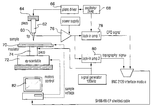
Figure 2 presents a schematic diagram of the instrument of an embodiment of
the
present invention. The system comprises of the following components: a
scanning system
having a tip (60), tip holder (62), piezoelectric element (64), piezoelectric
element driver
(66); vibrational frequency generator or oscillator (68), insulator (70), and
a scan table (72)
controlled by a micropositioner; a sample-tip distance control unit having a
piezoelectric
translation stage (74) and a capacitance-detection frequency generator; a
measurement system
having an ultra low-noise charge amplifier (76), a first Iocl~-in amplifier
(78) for measuring
the voltage and generating a contact potential difference image signal, a
second lock-in
amplifier.(80) for monitoring sample-tip distance and for generating a
topographic image
signal, vibrational frequency generator, and capacitance-detection frequency
generator; a
signal collection unit (82) having an interface module for interfacing the
measuring system
with a data acquisition (DAQ) board installed inside the computer; and a
computing device
for controlling the system.
A sample is placed on the scan table. The scan table is movable in the
directions of
the x-axis and the y-axis in order to have the sample scanned. The position of
the scan table is
adjusted by a micropositioning system (Nayaonics, Israel)) which moves the
scan table in x
and y directions with a coarse resolution of 100 nm (closed loop DC motor) and
a fine
resolution of 4 nxn (closed loop PZT drive), respectively. The control of the
micropositioning
system is achieved by a motor controller board installed in the computer. A
piezoelectrically
driven translation stage is mounted on the top of the scan table. The stage
moves along the z-
axis in order to maintain a constant distance between the tip and the sample.
CA 02447929 2003-11-21
WO 01/90730 PCT/CA01/00717
13
The tip is attached to the piezoelectric element via the tip holder. The
frequency of the
vibration, f , to vibrate the tip, is generated by a frequency generator
(oscillator) and is then
fed into the vibrating piezoelectric element (TopometYix, CA, U SA) through
the piezoelectric
driving amplifier (LP. Piezomeclaanik, GeYmany )
The Kelvin current extracted by the tip is converted to a voltage and
amplified by
means of an ultra low-noise preamplifier and a charge amplif er (A250 + A275,
Amptek Inc.
USA). This voltage is fed at the entrance of the two lock-in amplifiers.
The first lock-in amplifier (SR530, Stanford Research Systems, USA) is tuned
at fi
and used to obtain the CPD signal. The f may range from 1-20 kHz. The output
voltage of
the CPD lock-in amplifier is returned to the probe in a feedback loop (not
shown). For large
enough values of the open loop gain, the contact potential value is given
directly by the
output voltage of the lock-in amplifier.
The distance between the sample and the tip is monitored via capacitative
control at a
frequency above the vibration frequency fl. The f2 may range from 100-500
l~IIz. A small AC
voltage (100 mV at frequency, f2=100 kHz) is added in the circuit and the
resulting Kelvin
current between the tip and the sample is detected by a second lock-in-
amplifier (SR530,
Stanfond Research Systems, USA) tuned to f2. The tip-sample capacitance is
kept constant by
returning the output signal of the second lock-in amplifier to the
piezoelectric translation
stage. This signal is also used to obtain the topographical image of the
sample.
The data acquisition and signal processing is done with the data acquisition
board
(PCI-6110) installed in the computer. All electric cables are carefully
shielded and a BNC
2120 interface module is used for connections. The BNC 2120 interface module
is a
connector module interfacing the measuring system with the DAQ (data
acquisition) board
installed inside the computer. It contains a function generator, BNC
coimectors for analog
input chamlels, analog output, digital input/output
The system is controlled by a computing device having a PCI-6110 DAQ board
(Natioraal Instrufnents), the motor controller C-842.20DC and the LabView
programs
(version 6I).
The exterior compensating voltage reduces the Kelvin current to zero. To
measure the
CPD on a small scale with high precision it is necessary to control closely
the distance
between the tip and the sample. This has previously been achievedl by
separation of the
CA 02447929 2003-11-21
WO 01/90730 PCT/CA01/00717
14
harmonics of the Kelvin current. However, this prior art approach leads to
instability and is
unreliable. The SIAM system disclosed herein used instead a higher frequency
(sample-tip
capacitance detection) to control the sample-tip distance, thus, making the
process stable and
reliable.
1 The equipment construction, testing and adjustment of the prototype are
conducted to
ensure performance of the instrument and to assess its use in different
applications. In order
to calibrate the instrument and to verify the correct function, a number of
metallic surfaces
including Pt, Au, Ag, Sn, Pb and Al were examined. Patterned surfaces were
obtained by
sputtering of Pt layers on Ag and Si, Au layers on Pd and Ag, and metals on
silicon and mica
substrates. Conductive highly ordered-pyrolitic graphite and clean
semiconductor surfaces
(silicon) were also investigated. Contact potential images of dielectric
materials such as mica,
Teflon, silanized surfaces, NaCI and CsCI-treated substrates proved that the
instrument can
measure insulating surfaces. A theoretical explanation can be provided for
this particular kind
of measurement, based on combined dielectric layers of air and dielectric
material between
the metallic tip and the metallic table of the SKM. Biomolecules such as DNA,
collagen, and
other proteins deposited on different types of substrate were also studied.
A number of technical problems were solved in arriving at the SKM methodology
disclosed herein.
Tt was necessary to clarify the true basis of the measurement of work function
since
major discrepancies exist in the literature with respect to "calibration" of
contact potential
differences as the measured contact potential can be significantly altered by
the adsorption
and contamination of surface layers. Quantitative interpretation of such data
is difficult or
even meaningless as evidenced by the large discrepancies found in compilations
of work
function values. Experimental measurements of CPD found in the literature show
wide
variations (the value for gold, for example, ranges from 4.68 to 6.24 eV).
That is why, in
order to find absolute values of work function of different materials, a
special high-vacuum
chamber can be attached to the system and carefully cleaned surfaces are
beneficial are used.
However, many applications do not require absolute values of CPD. They require
only a
simple indication.of the electric charge distribution or a modified
configuration of the local
charges due to a subsequent physical or chemical treatment on the particular
surface under
investigation. These determinations can be performed in air and do not require
special
CA 02447929 2003-11-21
WO 01/90730 PCT/CA01/00717
IS
experimental conditions. This is the case with the SKM disclosed herein as an
embodiment of
the present invention, wluch is considered to constitute a major advantage
when it comes to
facile measurement performed without elaborate sample preparation.
Being a non-modulated SKM, the previous instrument was unable to fully
compensate
the measured CPD, since it depended on a voltage between the sample and tip to
generate a
' Kelvin current needed for the distance control circuit. The sample voltage,
a constant in the -
SV to +5V range, could not balance the real value of the CPD. A null-condition
(i.e., a perfect
match between the real value of the CPD and the existing sample voltage)
would, .thus, cause
a breakdown of the distance control system. Accordingly, the prior art
instrumentation did
not allow measurement of CPD directly. The CPD value generated by the
instrument was
near to, but was not the actual CPD. It was related to the CPD by a linear
function. By
conducting a two-point calibration, using two materials with a known and
stable worlc
function the inventors could determine the slope and offset of this line. By
applying the linear
function, the output of the SKM could be converted to the real value of the
CPD. However,
two-point calculation required for every measurement was time-consuming.
Further, the
inventors were confronted by the fact that an imperceptible change in any of
the relevant
parameters such as the vibration amplitude; sample voltage, tip size or mean
tip-sample
distance could altered the parameters of the linear function. Thus, the
calibration itself
became a potential source of errors. With the prior art instrumentationl, for
any change in
probe size, the Kelvin current would become so small that it would be
impossible to detect,
due to an extremely unfavorable signal/noise ratio. Further, due to outdated
electronic
solutions on the analog and digital circuitry the system soon became extremely
unstable
requiring considerable time to reliably generate clear and complete images.
For the reasons specified above and to benefit from recent advances in
electronic
technology, the inventors decided to build a modulated SKM that would obviate
one or more
problems described above and enable measurements under null-conditions. In
order to
achieve this, all electronic controls had to be modified by using high
performance devices
(such as charge amplifiers and lock-in amplifiers). This led to the inventive
instrumentation
disclosed herein.
The scanning Kelvin microprobe prototype was also modified to improve spatial
resolution. The initial 20-50 ~Cm resolution has been sigivf candy enhanced to
1 ~Cm by using
CA 02447929 2003-11-21
WO 01/90730 PCT/CA01/00717
16
sharper tungsten tips as probes. Additionally, to shield the electrode against
parasitic
electrical fields, guarded microelectrodes were developed. The shield is
interrupts the circular
lines of the electric field developing in the entire space between the
metallic tip and metallic
table by confining the field only in the apex aperture area. This also
improves the sensitivity
and lateral resolution of the probe. Electron microscopy is used to
characterize the quality of
the vapor deposition procedure used in order to form the guarded tip.
Figure 3 shows a flow chart of a software program developed to operate the
system
according to the invention. The software was developed in LabView language
(ve~sioJ2 6i,
National Instruments, USA) so the actual front panel of the SKM is displayed
on the
computer screen, the controls are available using the computer mouse, and the
measuring
develops in real time in graphic fashion on the screen, The virtual front
panel is supported by
the general block diagram behind it. The program controls the communication
protocols
between the hardware components, the motion of the micropositioning system,
the vibration
and translation of the tip and the piezoelectric table, the functioning of the
feedback loops and
I5 the whole data acquisition protocols, and saves the measured data in the
files. The measured
data are processed and analyzed using the image processing software (version
6.1,
OYiginLab, USA) to obtain 2D or 3D pictures of both CPD and topography images.
As illustrated in Figure 3, files are opened (90) to receive data relating to
either the
CPD image or the topography of the sample surface. A card and motor
initialization step
(92) allows for control of the SKM system. Data from the first and second lock-
in amplifiers
are obtained (94) and tip movement (96) in the z direction to approach the
sample is effected
on this basis. The sample is scanned (98), and the tip can be moved in the z
direction (100) to
retract from the sample. The data obtained is written to the files opened
(102), and the
process may be either repeated or terminated, in which case the file is closed
(104).
EXAMPLES
The invention is further described, for illustrative purposes, in the
following specific
Examples.
CA 02447929 2003-11-21
WO 01/90730 PCT/CA01/00717
17
Example 1
Clzaracteriziizg Metals
A number of metallic surfaces including Pt, Au, Ag, Sn, Pb and Al are
examined.
Patterned surfaces are obtained by sputtering of Pt layers on Ag and Si, Au
layers on Pd and
Ag, and metals on silicon and mica substrates.
Figure 4 illustrates a CPD image obtained from a silver surface. Figure 5 is a
CPD image of
a silver surface after surface treatment. Figure 6 is a CPD image of silver on
a mica surface. Figure 7
illustrates the topography of silver on a mica surface.
Exa~zple 2
Claaracterizing Conductors
Highly ordered-pyrolitic graphite samples are analyzed. Figure 8 illustrates
the topography of a graplute surface. Figure 9 is a CPD image of a highly-
ordered pyrolitic
graphite surface. .
Exa~raple 3
Microelectronic Fabrication
Figures 10A and 10B show a measure of the capabilities of the instrument by
providing a tandem measurement of topography and CPD. Figure I OA depicts a
topographical image of the edge presented by a layer of aluminum deposited on
a silicon
wafer in a typical microelectronic fabrication process. The edge is supposed
to be vertical
with a steep height of about 1 Vim. This particular topographical image was
realised at'a
spatial resolution of 2 pm. Note that the second axis represents (in V) the
displacement of
the piezoelectric table and for 1V the piezoelectric material expands 20 pm.
Accordingly, the
aluminum layer appears to have a surface height variation of about 400rim
(0.02V). Secondly,
it can be seen that the edge actually slopes over 20 ~.m (x-axis). Figure lOB
shows a tandem
CPD image. Note that the image is both rotated at 90° and inverted in
order to highlight the
difference in contact potential between aluminum and silicon (the flat, bottom
surface
situated at 1.5V CPD is the aluminum surface). The technique as described
herein does not
generate absolute values of contact potential difference. Accordingly, the z-
axis represents a
relative scale of CPD values.
CA 02447929 2003-11-21
WO 01/90730 PCT/CA01/00717
18
Example 4
Biosehsor Teclzhology
Reagents. The following chemicals were obtained from Aldrich and used as
received:
c~-Undecanoyl alcohol 98%, 6,6'-dithiodinicotinic acid, trifluoroacetic
anhydride 99%,
hydrogen hexachloroplatinate (IV) 99.99%, octadecyltrichlorosilane (OTS),
trichlorosilane
99%, 3-mercaptopropyltrimethoxysilane (MPS), N-bromosuccinimide (NBS),1,1'-
azobis-
(cyclohexanecarbonitrile)(ACN), and dimethylformamide-sulfurtrioxide complex.
Various
common solvents and chemicals were obtained from BDH and used without further
treatment
unless otherwise indicated as follows. Dichloromethane and acetonitrile,
toluene and pyridine
were distilled over P205, Na and KOH, respectively, and benzene and DMF were
dried over
molecular sieves before use.
Syntheses. 1-(thiotrifluoroacetato)-11-(trichlorosilyl)-undecane (TTU) was
synthesized and characterized as described previouslyl6-i9. The sodium salt of
2.5-bis
(bromomethyl) benzensulfonate (BMBS) was produced by bromomethylation of p-
xylene
followed by conversion to the sulfonate (sodium salt) with DMF-sulfurtrioxide
reagent and
NaOH.
Oligonucleotide syntheses of the following thiolated sequences 5'-HS-C6--
TATAAAAAGAGAGAGATCGAGTC-3' (Fl) and its single strand, un-thiolated complement
(F2), were performed using standard CE phosphoroamidite chemistry with
conventional
Applied Biosystems Ihc. reagents. In order to produce the thiol-group
containing
oligonucleotide, an iodine solution was employed in conjunction with 3'-thiol
modification
cartridges (Glen Research). The oligonucleotides were purified using standard
procedures
with Poly-Pak cartridges purchased from Glen Research. The final products were
checked for
purity by HPLC and stored in 20% acetonitrile, in polypropylene vials.
Solutions of F1 were
treated with a ten-fold excess of BMBS at neutral pH in order to produce an
oligonucleotide-
linker complex.
Procedures. Silicon surfaces were silanized in a dry box for 2 hours with 2 ml
of a
10-3 M solution in dry toluene of a mixture of 30% TTU / 70% OTS. The TTU
coated wafers
were treated with hydroxylamine in water (pH 8.5) for 2 hours to effect
deprotection of the
thiol group. The Fl oligonucleotide was attached to the surface via the linker
BMBS as
CA 02447929 2003-11-21
WO 01/90730 PCT/CA01/00717
19
described elsewherel9. Hybridization of the surface-bound oligonucleotide with
its
complementary strand was effected in pH 7.5 buffer at room temperature.
Surface iffZmobilization of 25-mer oligohucleotides. The design and
fabrication of
biosensors capable of the detection of interfacial nucleic acid hybridization
and interaction
with small molecules such as drugs, regulatory peptides is an important area
of study. This
research activity requires the attachment of single strands of
oligonucleotides to the device
surface. A protocol extensively for achieving this involves nucleic acid-
surface binding
though interaction of chemisorbed neutravidin with biotinylated
oligonucleotide. This method
produces a surface nucleic acid density of only, at best, 1 pmol cm z
(compared to the
maximum possible, for single strands, of about 100 pmol cnri Z) 18. However,
the sensitivity of
device response can be enhanced by increasing nucleic acid surface density
through
silanization technology (on sensor chromium electrodes). The silane employed
in the present
experiments, to increase nucleic acid surface density, TTU, attaches to
hydroxylated
substrates by a self assembly process to produce a near monolayer-like array
of thiol
functionalities (following de-protection of the sulfur-containing moieties).
Dilution with OTS
serves to minimize thiol-group cross linking interactions, and the use of a
linlcing agent that
forms disulfide bonds such as BMBS was found to optimize surface density of 11-
mer
oligonucleotides at~about 50 pmol cm 2 on silicon wafersl9.
Silicon wafers obtained from International Wafer Service were supplied
approximately 0.4 thick and were polished on one side to a mirror finish. They
were cut to a
size of about 1x1 cm using a diamond-tipped pencil. This experiment was
conducted to
obtain images that can serve as a control for any changes produced by
subsequent surface
chemical treatments. Figures 1IA and 11B show the tandem topographical and CPD
images
obtained at 20 ~m spatial resolution for the bare silicon wafer, respectively.
The silicon wafer
was later used for immobilizing nucleic acids. With respect to the
topograplucal image, the
picture was recorded viewing from the y-axis in order to isolate an obvious
fissure of depth
about 800 nm (width at half depth is 100 ~.m). Aside from this structure,
which is likely
related to scratching connected to a polishing protocol, the surface height
variability is of the
order of 300 nm (0.15 V). The image also exhibits fairly uniform "peaks" with
a half height
dimension of about 100 nm. These characteristics are expected from a substrate
surface that
is considered to be optically flat. The CPD image shows a quite narrow range
of surface
CA 02447929 2003-11-21
WO 01/90730 PCT/CA01/00717
variability of approximately of 75 mV, which is likely connected to
differences in the level of
oxidation and/or contamination from adventitious carbon. Note that the
features on terms of
spatial characteristics reflect the same overall picture as shown for the
topographical image.
The immobilization of nucleic acids on biosensors and gene chips using TTU
5 represents a new research area. The attachment of oligonucleotides to a
silicon substrate was
tested by employing the capabilities of the new SKM instrument.
With respect to the use of Kelvin probe measurements to distinguish
oligonucleotide
and DNA duplex formation, the 25-rner probe, Fl, with BMBS linker in place,
attaches to the
de-protected TTU monolayer on the Si wafer through formation of a disulfide
bond. Using
10 this approach, the probe is disposed closer to the substrate surface at the
S'-end, whereas the
3'-terminus faces away from the interface. Experience has shown that the
surface packing
density attainable by this attachment protocol is of the order of 20 pmol cm
2' This value
implies that the surface density of attached nucleic acid is in the region of
1 molecule per 10
square nanometers. The precise orientation of the probe is unknown in terms of
the air-to-
15 solid interface. Figure 12 shows the CPD image of Si surface-attached Fl (1
~,m resolution).
The surface variability is in the range of about 100 mV with the mean value
being 1.70 V.
This represents a shift of approx. 80 mV per the average CPD value for the
bare Si surface.
There are "peaks" depicted in the image with widths at half height of about 7
~.m (spaced by
10 Vim).
20 Figure 13 shows the CPD image of the same surface for F2 hybridized to Fl.
The
overall surface variability and features are much the same as for the single
strand 25-mer
attached to the substrate, but the CPD value has shifted upward by over 200
mV. This result
clearly indicates that detection of duplex formation by the SKM is feasible.
Since the
attainable resolution in relative CPD value is 1 mV, this result implies that
high
discrimination of the level of duplex formation connected to mismatches is
feasible.
Example 5
MicfofnaclZined Devices, Thih Filsfzs, ahd Self Assembled Monolayers
This example is illustrative of the application of SKM according to the
invention in
characterization of micromachined devices, thin-films, and self assembled
monolayers. The
properties of materials that form thin-films, self assembled monolayers and
microscopical
CA 02447929 2003-11-21
WO 01/90730 PCT/CA01/00717
21
structures appear to be different from those of a bulk material. Not only is
scaling important
in determining material and device properties in the micro-world, but also
important are the
relations between electrical and structural properties of the surface.
Moreover,
microminiaturization blurs the distinction between physical and chemical
properties. Thus,
the availability of new methods and advanced techniques for material
characterization and
device performance in the micro- and nano-worlds becomes imperative. SKM
provides such
a new technique, by offering a tandem electrical (through CPD measurements)
and structural
(topology) characterization.
Figures 14 and 15 illustrate the application of SKM in micromachining. Figure
14
represents a topographical image of micromachined structures patterned by
laser
micromachined technology on a TSM (Thickness-Shear Mode) sensor which were
detected
' by the SKM technology disclosed here. Figure 14 shows the image of a one
channel of 5 ~m
width in the silicon surface Laser micromachining was used with a 5 micron
line, a 40 micron
space, and with a 1 micron lateral step. Figure 15 shows the image of five
channels of 5 ~,m
width in the silicon surface. The 5 pm channels were formed in the silicon
surface to change
the electric field density, hence enhancing the signal and improving the
functioning of the
TSM . Lines of 5 micron were laser micromachined with a 1 micron lateral step.
The SIAM
technology is facilitating the synergy provided by silicon fabrication
techniques and
biomolecule deposition to medical sensor devices in developing new
applications and
products of commercial interest.
Example 6
Claaracterizihg Corroded Substrates
SKM can be employed in characterizing corroded substrates, with no special
requirements being necessary. The measurement principle is based on the
relationship
between the surface potential and the corrosion potential, through the charge
and dipole
distribution at the interfaces. The SKM instrument can be used to obtain high
lateral
resolution that is needed to understand corrosion phenomena at micro- and nano-
metric
levels. Usual surface-analytical techniques can be used concomitantly.
In order to examine the potential of SKM in detecting corrosion, a piece of
metal from
Coca-Cola pop-can was investigated to assess the integrity of the paiilt layer
that isolates the
CA 02447929 2003-11-21
WO 01/90730 PCT/CA01/00717
22
A1 wall from the liquid, thus preventing the leaching of aluminum oxides
(known as liver
poisons) into the liquid. Images generated by SKM technology showed large
islands of
removed paint corroded by the liquid.
B'xample 7
Application in Determining Biocompatibility of Materials
SKM was employed to determine biocompatibility of materials. Figure 16A and
16B show
CPD images of samples of silicone polymer used in breast implants. The samples
were from
breast implants that were surgically removed from a patient who chose
explantation due to
~ controversy surrounding the medical consequences of silicon polymer-based-
breast implants.
Both the samples were obainted from the same implant. However, the one used
for the image
shown in Figure 16A was isolated from the inside surface of the structure of
the implant
closest to the chest cavity, whereas the one used for the image shown in
Figure 16B was in
contact with biological tissue towards the outside. The images demonstrate the
power of the
capability of SIAM to represent CPD on a pseudo three-dimensional basis, that
is, with spatial
(xy plane) data plotted together with variation in actual CPD level (z plane).
It is clear from
the images that the surface exposed to different tissues possesses not only
altered level of
CPD, but also more variation than the other sample. Specifically, on average,
the CPD values
for the former surface aresomewhat lower than the latter. In contrast, the
topographical
images of these samples exhibited identical smooth surfaces. The result
demonstrates that the
SKM can examine surface functional group chemistry, at the sub-micrometer
level.
REFERENCES
1. L-E. Cheran, H-D. Liess, M. Thompson, The Analyst, 1999,124, 961.
2. W. Nabhan, B. Eqer, A. Broniatowski and G. De Rosny, Rev. Sci. Instrum.,
1997, 68 (8),
3108.
3. M. Schmidt, M. Nohlen, G.,Bermes, M. Bomer and I~. Waaidelt, Rev. Sci.
Instrum., 1997,
68, 10, 3866.
4. M. Bomisch, F. Burmeister, A. Rettenberg, J. Zimmermann , J. Boneberg and
P.
Leiderer, J. Phys. Chem. B, 1997,101, 10162.
5. W.A. Zissman, Rev. Sci. InstYUm., 1932, 3, 367.
CA 02447929 2003-11-21
WO 01/90730 PCT/CA01/00717
23
6. P. Craig and V.Radeka, Rev. Sci. Ihst~um., 1970, 41, 2, 258.
7. N.A.Surplice and R.J. D'Arcy, J.Phys.E: Sci. Instrum., 3, (1970), 477.
8. B. Ritty, F. Watchel, R. Manquenouille, F. Ott, J. Bonnet, J. Phys. E:
Sci.Inst~um.,15,
1982, 310.
9. LD. Baikie, E. Venderbosch, Rev.Sci.Instrum. 62 (3), 1991, 725.
10. 0.A. Semenikhin, L.Jiang, T. Iyoda, K. Hashimoto, A. Fujishima, J. Phys.
Chem. 100,
48, 1996, 18603.
11. I. Samec. W. Johnson, M. Cappadonia, M.Jauch, K. Doblhofer, SensoYS and
Actuators, B,
13-14 (1993) 741.
12. S. Lundgren, B. Kasemo,Rev. Sci.Instrum. 66, 7, (1995) 3976.
13. C. S. Kumar, A. Subrahmanyarn, J. lVlajhi, Rev. Sci. histrum. 67 (3)
(1996), 805.
14. H.A. Engelhardt, P. Feuhzer, H. Pfniix, D. Menzel, J. Phys E: Sci. Inst..
19, (1977), 1133.
15. LD. Baikie, G.H. Bruggink, Mat. Res. Soc. Syn2p. PYOC. 309, (1993), 35.
16. M. E. McGovern, M. Thompson, Can.J.Chem. 77 (1999), 1678.
17. L.M. Furtado, H.Su, M. Thompson, D.P. Mack, G.L. Hayword, Anal. Chern. 7,
(1999),
1167.
18. M. E. McGovern, M. Thompson, Anal. Chem. Submitted.
19. 20. M. NonneiZlnacher, M.P. O'Boyle and H.K. Wickramasinghe, Appl. Phys,
Lett., 1991,
58, 25, 2921.
20. M. Nomlemnacher, M.P. O'Boyle and H.K. Wickramasinghe, Ultramic~oscopy,
1992, 42-
44, 268.
21. M.Yasutake, J. Appl. Phys., 1995, 34, 3403.
22. M.Yasutake, A.Daisuke and M. Fujihira, Thin Solid Films, 1996, 723, 279.
The above-described embodiments of the present invention are intended to be
examples only. Alterations, modifcations and variations may be effected to the
particular
embodiments by those of skill in the art without departing from the scope of
the invention,
which is defined solely by the claims appended hereto.