Language selection

Search

Patent 2448939 Summary

Third-party information liability

Some of the information on this Web page has been provided by external sources. The Government of Canada is not responsible for the accuracy, reliability or currency of the information supplied by external sources. Users wishing to rely upon this information should consult directly with the source of the information. Content provided by external sources is not subject to official languages, privacy and accessibility requirements.

Claims and Abstract availability

Any discrepancies in the text and image of the Claims and Abstract are due to differing posting times. Text of the Claims and Abstract are posted:

  • At the time the application is open to public inspection;
  • At the time of issue of the patent (grant).
(12) Patent: (11) CA 2448939
(54) English Title: CONNECTOR
(54) French Title: CONNECTEUR
Status: Expired and beyond the Period of Reversal
Bibliographic Data
(51) International Patent Classification (IPC):
  • H01R 11/01 (2006.01)
  • H01R 13/00 (2006.01)
  • H01R 13/02 (2006.01)
  • H01R 13/405 (2006.01)
  • H01R 13/52 (2006.01)
  • H01R 43/16 (2006.01)
  • H01R 43/18 (2006.01)
  • H01R 43/24 (2006.01)
(72) Inventors :
  • ALDRIDGE, IAN EDWARD (United Kingdom)
(73) Owners :
  • CONTOUR ELECTRONICS LIMITED
(71) Applicants :
  • CONTOUR ELECTRONICS LIMITED (United Kingdom)
(74) Agent: FINLAYSON & SINGLEHURST
(74) Associate agent:
(45) Issued: 2007-11-06
(22) Filed Date: 2003-11-12
(41) Open to Public Inspection: 2004-05-13
Examination requested: 2003-11-12
Availability of licence: N/A
Dedicated to the Public: N/A
(25) Language of filing: English

Patent Cooperation Treaty (PCT): No

(30) Application Priority Data:
Application No. Country/Territory Date
0226479.4 (United Kingdom) 2002-11-13

Abstracts

English Abstract

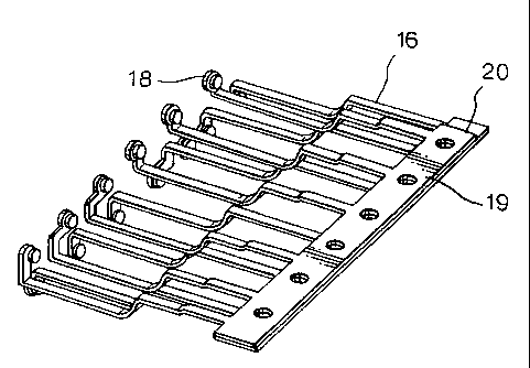
A connector comprising a body; a plurality of terminals and a plurality of signal contacts. The terminals are arranged in two substantially parallel rows on one face of the body. A signal contact is connected to each terminal and all of the signal contact extend from another face of the body in a single row substantially parallel to the row of terminals.


French Abstract

Un connecteur qui comprend un corps, une pluralité de terminaux et une pluralité de contacts émetteurs. Les terminaux sont disposés en deux rangées substantiellement parallèles sur une face du corps. Un contact émetteur est raccordé à chaque terminal et tous les contacts émetteurs se prolongent de l'autre face du corps sur une seule rangée substantiellement parallèle à la rangée de terminaux.

Claims

Note: Claims are shown in the official language in which they were submitted.


WHAT IS CLAIMED IS:
1. An array of signal contacts for a connector, the array comprising:
two subarrays of contacts, each contact having a terminal at one end;
wherein the terminals of each respective subarray are disposed in separate
rows parallel
to one another;
each subarray having a respective removable end strip having a positioning
means for
holding the subarrays substantially parallel to another;
wherein said positioning means are adapted to be aligned such that, when
pressure is
applied, a single array is formed with said signal contacts in a single row;
and
wherein said array is adapted to being insert moulded into a connector body.
2. A connector comprising:
a connector body and an array of signal contacts according to claim 1.
3. The connector according to claim 2, further comprising a plurality of power
contacts
connected to the body and extending in a row substantially parallel to the row
of signal contacts.
4. A method of manufacturing an array of signal contacts for a connector, the
method
comprising the steps of:
forming two subarrays of contacts, each contact having a terminal at one end,
wherein the
subarrays are held substantially parallel to one another by respective end
strips each having
positioning means; and wherein the terminals of each respective sub-array are
disposed in separate
rows parallel to one another;
lining up the positioning means on the two subarrays;
pressing the end strips together so that the sub-arrays form a single array
with the signal
contacts in a single row;
insert moulding the terminals in a connector body; and thereafter
removing the end strips from the signal contacts.
-4-

A method of manufacturing a connector comprising steps of:
manufacturing an array according to the method of claim 4,
insert moulding a set of power contacts having a end strip into the connector
body; and
removing the end strip from the power contacts.
6. A method of manufacture according to claim 3 or claim 4 wherein the
positioning means
comprise at least one recess on one subarray and at least one projection on
the other subarray.
-5-

Description

Note: Descriptions are shown in the official language in which they were submitted.


CA 02448939 2006-07-19
CONNECTOR
This invention relates to a power connector and a method of manufacturing
the connector.
The aim of the present invention is to provide a compact connector which
incorporates both power and signal contacts within a single housing. In the
past
it has proved difficult to deliver the required combination of power and
signal
contacts whilst fulfilling both the space constraints and the IP67 standard
for water
sealing.
According to the present invention there is provided an array of signal
contacts for a connector, the array comprising: two subarrays of contacts,
each
contact having a terminal at one end; wherein the terminals of each respective
subarray are disposed in separate rows parallel to one another; each subarray
having a respective removable end strip having a positioning means for holding
the subarrays substantially parallel to another wherein said positioning means
are
capable of being aligned such that, when pressure is applied, a single array
is
formed with said signal contacts in a single row; and wherein said array is
capable
of being insert moulded into a connector body.
Preferably, the connector further comprises a plurality of power contacts
connected to the body and extending in a row substantially parallel to the row
of
signal contacts.
According to the present invention there is further provided a method of
manufacturing an array of signal contacts for a connector, the method
comprising
the steps of: forming two subarrays of contacts, each contact having a
terminal at
one end, wherein the subarrays are held substantially parallel to one another
by
respective end strips each having positioning means; and wherein the terminals
of
each respective sub-array are disposed in separate rows parallel to one
another;
-1-

CA 02448939 2006-07-19
lining up the positioning means on the two subarrays; pressing the end strips
together so that the sub-arrays form a single array with the signal contacts
in a
single row; insert moulding the terminals in a connector body; and thereafter
removing the end strips from the signal contacts.
A method of manufacturing a connector may provided comprising steps of:
manufacturing an array as detailed above, insert moulding a set of power
contacts
having a end strip into the connector body; and removing the end strip from
the
power contacts.
Preferably, the positioning means comprise a recess on one subarray and
a projection on the other.
An example of a connector according to the present invention will now be
described with reference to the accompanying drawings in which:
Figure 1 shows two subarrays of signal contacts;
Figure 2 shows the two subarrays combined to form a single array;
Figure 3 shows an array insert moulded into a body;
Figure 4 shows a front face of a body;
Figure 5 shows an array and a body once an end strip has been removed;
Figure 6 shows a power contacts insert moulded into a body;
-lA-

CA 02448939 2003-11-12
Figure 7 shows a connector once the power contact end strip has been removed;
Figure 8 shows a completed connector according to the present invention.
In Figure 8 is shown a completed connector 10 comprising a body 11 with two
rows of holes 14, 15 for terminal contacts on the front face 12 thereof. The
two rows of
holes 14,15 are substantially parallel. Extending from the rear face 13 of the
body 11 is
an array of elongate signal contacts 16. An array of elongate power contacts
17 also
extends from the rear face 13 of the body 11. The array of power contacts 17
is
substantially parallel to the array of signal contacts 16.
The method steps used to manufacture the connector 10 shown in Figure 8 are
shown in Figures 1 to 7.
Figure 1 shows two subarrays of elongate signal contacts 16a, 16b. Each signal
contact has a terminal 18 at one end and is formed from phosphor bronze or a
copper
alloy, and the signal contacts of each subarray 16a, 16b are held in a
substantially parallel
configuration by respective end strips 19a, 19b. On the end strips 19a, 19b
there are
respective positioning means 20a, 20b, in the form of a series of recesses 20a
and a
series of projections 20b. The positioning means 20a, 20b allow the two end
strips to be
engaged with one another so that the subarrays of signal contacts 16a, 16b are
lined up
so that they form a single array 16. As a result of the configuration of the
signal contacts,
the terminals 18 are in two substantially parallel rows. Figure 2 shows the
single array 16.
This array of signal contacts 16 is then insert moulded onto a plastics,
insulating
body 11 as shown in Figure 3. The insert moulding process involves inserting
the body
11 into a mould and moulding material, preferably PBT 15% glass filled UL94-
VO, around
it in order to connect the terminals 18 of the signal contacts 16 with the two
rows of holes
14, 15 in the body 11 (shown in Figure 4) such that the signal contacts extend
in an array
16 from the rear face 13 of the body 11.
Once this insert moulding process is complete the end strips 19 can be removed
to leave one substantially parallel array of signal contacts 16 extending from
the rear face
13 of the body 10. This is shown in Figure 5.
A further process of insert moulding is then undertaken to mould an array of
power
contacts 17 into the body 11. This is shown in Figure 6. The moulding material
is
preferably PA6T 15% glass filled UL94-VO. The moulding material is different
from the
material used in the first phase of insert moulding to ensure that the front
face of the
connector does not bow. It is also possible to alter the thicknesses of the
first and second
stage insert moulding (whilst maintaining the same overall thickness) in order
to ensure
that the front face does not bow. The power contacts 17 are held in a
substantially
parallel array by an end strip 21 and the moulding results in the array of
power contacts
17 being substantially parallel to the array of signal contacts 16 extending
from the
-2-

CA 02448939 2003-11-12
reverse face 13 of the body 11. Once the insert moulding process is complete
the end
strip 21 is removed as shown in Figure 7.
The signal contacts 16 are then bent into the desired shape on the rear of the
body
11.
-3-

Representative Drawing
A single figure which represents the drawing illustrating the invention.
Administrative Status

2024-08-01:As part of the Next Generation Patents (NGP) transition, the Canadian Patents Database (CPD) now contains a more detailed Event History, which replicates the Event Log of our new back-office solution.

Please note that "Inactive:" events refers to events no longer in use in our new back-office solution.

For a clearer understanding of the status of the application/patent presented on this page, the site Disclaimer , as well as the definitions for Patent , Event History , Maintenance Fee  and Payment History  should be consulted.

Event History

Description Date
Time Limit for Reversal Expired 2017-11-14
Letter Sent 2016-11-14
Inactive: Late MF processed 2013-03-20
Maintenance Request Received 2013-03-20
Letter Sent 2012-11-13
Grant by Issuance 2007-11-06
Inactive: Cover page published 2007-11-05
Pre-grant 2007-08-21
Inactive: Final fee received 2007-08-21
Notice of Allowance is Issued 2007-03-12
Letter Sent 2007-03-12
Notice of Allowance is Issued 2007-03-12
Inactive: Approved for allowance (AFA) 2007-02-26
Amendment Received - Voluntary Amendment 2006-07-19
Inactive: IPC from MCD 2006-03-12
Inactive: S.30(2) Rules - Examiner requisition 2006-01-26
Inactive: Office letter 2006-01-16
Inactive: Delete abandonment 2006-01-12
Deemed Abandoned - Failure to Respond to Maintenance Fee Notice 2005-11-14
Application Published (Open to Public Inspection) 2004-05-13
Inactive: Cover page published 2004-05-12
Inactive: IPC assigned 2004-01-20
Inactive: First IPC assigned 2004-01-20
Inactive: IPC assigned 2004-01-20
Inactive: First IPC assigned 2004-01-20
Inactive: Filing certificate - RFE (English) 2003-12-19
Filing Requirements Determined Compliant 2003-12-19
Letter Sent 2003-12-19
Letter Sent 2003-12-17
Application Received - Regular National 2003-12-17
Request for Examination Requirements Determined Compliant 2003-11-12
All Requirements for Examination Determined Compliant 2003-11-12

Abandonment History

Abandonment Date Reason Reinstatement Date
2005-11-14

Maintenance Fee

The last payment was received on 2007-10-11

Note : If the full payment has not been received on or before the date indicated, a further fee may be required which may be one of the following

  • the reinstatement fee;
  • the late payment fee; or
  • additional fee to reverse deemed expiry.

Please refer to the CIPO Patent Fees web page to see all current fee amounts.

Owners on Record

Note: Records showing the ownership history in alphabetical order.

Current Owners on Record
CONTOUR ELECTRONICS LIMITED
Past Owners on Record
IAN EDWARD ALDRIDGE
Past Owners that do not appear in the "Owners on Record" listing will appear in other documentation within the application.
Documents

To view selected files, please enter reCAPTCHA code :


To view images, click a link in the Document Description column. To download the documents, select one or more checkboxes in the first column and then click the "Download Selected in PDF format (Zip Archive)" or the "Download Selected as Single PDF" button.

List of published and non-published patent-specific documents on the CPD .

If you have any difficulty accessing content, you can call the Client Service Centre at 1-866-997-1936 or send them an e-mail at CIPO Client Service Centre.


Document
Description 
Date
(yyyy-mm-dd) 
Number of pages   Size of Image (KB) 
Description 2003-11-12 3 148
Abstract 2003-11-12 1 11
Claims 2003-11-12 1 45
Drawings 2003-11-12 4 172
Representative drawing 2004-01-27 1 25
Cover Page 2004-04-16 1 47
Description 2006-07-19 4 152
Drawings 2006-07-19 4 166
Claims 2006-07-19 2 50
Representative drawing 2007-10-11 1 26
Cover Page 2007-10-11 1 51
Acknowledgement of Request for Examination 2003-12-17 1 188
Courtesy - Certificate of registration (related document(s)) 2003-12-19 1 125
Filing Certificate (English) 2003-12-19 1 170
Reminder of maintenance fee due 2005-07-13 1 109
Commissioner's Notice - Application Found Allowable 2007-03-12 1 162
Maintenance Fee Notice 2012-12-27 1 170
Late Payment Acknowledgement 2013-03-26 1 164
Maintenance Fee Notice 2016-12-28 1 178
Correspondence 2006-01-16 1 12
Correspondence 2007-08-21 1 34
Fees 2013-03-20 1 42