Note: Descriptions are shown in the official language in which they were submitted.
CA 02448945 2003-11-28
WO 03/005078 PCT/US02/13582
SYSTEM AND METHOD FOR FABRICATING ARRAYED
OPTICAL FIBER COLLIMATORS
BACKGROUND OF THE INVENTION
Field of the Invention
The present invention is generally directed to arrayed optical fiber
collimators and,
more specifically, a system and method for fabricating arrayed optical fiber
collimators.
Technical Background
Arrayed optical fiber collimators are increasingly utilized in optical
systems. For
example, arrayed optical fiber collimators have been used or proposed for use
in
conjunction with various optical chips, e.g., optical isolator chips and
optical circulator
chips. Due to the recent increase in demand for arrayed optical devices to be
used in dense
wavelength division multiplexing (DWDM) systems, reducing the arrayed optical
device
cost has become increasingly important. However, the effectiveness of optical
devices that
use collimating arrays, incorporating graded-index (GRIN), aspheric or Fresnel
microlenses, are highly dependent on the configuration of a given optical
fiber collimator
array. As such, it is important to configure the fiber collimator array to
reduce optical
losses.
What is needed is a system and method for aligning components of an arrayed
optical fiber collimator that is practical and minimizes optical losses.
SUMMARY OF THE INVENTION
The present invention is directed to a system and method for actively aligning
components of an arrayed optical fiber collimator. Initially, a first fixture
is provided for
receiving and retaining an optical fiber array block, which receives and
retains a plurality
of individual optical fibers. Next, a second fixture is provided for receiving
and retaining a
microlens array substrate that includes a plurality of microlenses integrated
along a
microlens surface and a substrate surface opposite the microlens surface.
Then, a third
fixture is provided for receiving and retaining at least a portion of a first
light receiver that
is positioned to receive a light beam from at least one of the integrated
microlenses. Next,
at least one light beam is provided from the light source to at least one of
the plurality of
individual optical fibers. The relative position of at least one of the
microlens array
CA 02448945 2003-11-28
WO 03/005078 PCT/US02/13582
2
substrate and the optical fiber array block is then adjusted to maximize the
optical power of
the light beam received by the first light receiver. Finally, a finished
arrayed optical fiber
collimator is provided by fixing the optical fiber array block to the
microlens array
substrate when the optical power provided by the integrated microlens is at a
maximum.
Additional features and advantages of the invention will be set forth in the
detailed
description which follows and will be apparent to those skilled in the art
from the
description or recognized by practicing the invention as described in the
description which
follows together with the claims and appended drawings.
It is to be understood that the foregoing description is exemplary of the
invention
only and is intended to provide an overview for the understanding of the
nature and
character of the invention as it is defined by the claims. The accompanying
drawings are
included to provide a further understanding of the invention and are
incorporated and
constitute part of this specification. The drawings illustrate various
features and
embodiments of the invention which, together with their description serve to
explain the
principals and operation of the invention.
BRIEF DESCRIPTION OF THE DRAWINGS
Fig. 1 is a perspective view of an arrayed optical device, according to an
embodiment of the present invention;
Figs. 2A-2C are diagrams of a setup for aligning an optical fiber array block
and a
microlens array substrate, according to an embodiment of the present
invention;
Fig. 3 is a graph depicting coupling loss as a function of spacing for a pair
of
arrayed optical fiber collimators whose components were aligned by a single-
mode
collimated (SMC) fiber procedure and a stepping procedure, according to
embodiments of
the present invention;
Fig. 4 is a block diagram of a setup for aligning an optical fiber array block
with a
microlens array substrate, according to another embodiment of the present
invention;
Fig. 5 is a graph depicting coupling loss as a function of spacing using the
SMC
fiber procedure, the stepping procedure, and the mirror procedure;
CA 02448945 2003-11-28
WO 03/005078 PCT/US02/13582
3
Fig. 6 is a graph depicting coupling loss increase as a function of time for
the setup
of Fig. 4;
Fig. 7 is a top view diagram depicting movement of the optical fiber array
block
and the mirror of Fig. 4 in relation to the microlens array substrate;
Fig. 8 is a block diagram of another setup for aligning components of an
arrayed
optical fiber collimator, according to another embodiment of the present
invention;
Fig. 9 is a graph depicting coupling loss as a function of distance for a
number of
collimator pairs constructed using the setup of Fig. 8;
Fig. 10 is a diagram of an arrayed optical fiber collimator that uses a
slanted
dummy block with a sloped surface to mate a slanted surface of the microlens
array
substrate;
Fig. 11 is a side view of an arrayed optical fiber collimator that uses a
dummy
block with a dent for acceptance of a convex-type or a diffractive microlens;
and
Fig. 12 is a side view of an arrayed optical fiber collimator that includes a
dummy
block with a sloped back surface, which is used with collimators that have a
collimated
light beam that is aligned at a few degrees deviated from the optical axis of
the microlens.
DETAILED DESCRIPTION OF THE PREFERRED EMBODIMENT(S)
Fig. 1 shows an arrayed optical device 100 that includes a first arrayed
optical fiber
collimator 102 and a second arrayed optical fiber collimator 112. The first
arrayed optical
fiber collimator 102 includes a first optical fiber array block 104, which
retains a plurality
of optical fibers 101, and a first microlens array substrate 106, which
includes a plurality of
microlenses integrated along a microlens surface. The second arrayed optical
fiber
collimator 112 includes a second optical fiber array block 114, which retains
a second
plurality of optical fibers 111, and a second microlens array substrate 116,
which includes
a plurality of microlenses integrated along a microlens surface. An optical
chip (e.g., an
isolator chip, a circulator chip, filter, etc.) 108 is retained within a
groove 118 formed in
substrate 120. Both the first arrayed optical fiber collimator 102 and the
second arrayed
optical fiber collimator 114 are coupled (e.g., with an adhesive) to the
substrate 120 such
that they are fixed in relation to each other and the chip 108 after
alignment.
CA 02448945 2003-11-28
WO 03/005078 PCT/US02/13582
4
Moving to Fig. 2, a procedure for aligning an optical fiber array block 202,
which
retains a plurality of optical fibers 201 (e.g., eight optical fibers), with a
microlens array
substrate 206 is depicted. The fibers 201 are coupled to a light source 214
that preferably
provides a light beam to each of the fibers 201. Alternatively, the light
source 214 may
only provide a light beam to fibers 201 at each end. As shown in Fig. 2A, a
first fixture
203 receives and retains the block 202 and is coupled to an auto-aligner 220
to facilitate
movement of the block 202 with respect to substrate 206 and a single mode
collimated
(SMC) optical fiber 210. The substrate 206 is received and retained by a
second fixture
205, which attaches the substrate 206 to the auto-aligner 220 facilitating
movement of the
substrate 206 by the auto-aligner 220. The SMC optical fiber 210 is coupled to
a receiver
212 and is received and retained by a fixture 207. The block 202 and the
substrate 206 are
adjusted in relation to each other to achieve maximum optical power from each
fiber 201
and its corresponding microlens, as seen by the receiver 212 (through the SMC
optical
fiber 210). It will be appreciated that to achieve optimal alignment between
the plurality of
optical fibers 201 of the block 202 and microlenses of the substrate 206
requires precise
indexing by the auto-aligner 220. When a desired alignment is achieved, the
block 202 is
affixed (e.g., with an optical adhesive) to the substrate 206, which provides
a finished
arrayed optical fiber collimator 230 that is utilized in conjunction with the
procedure of
Fig. 2B.
As shown in Fig. 2B, the plurality of optical fibers 201 of the collimator 230
are
coupled to the receiver 212. The collimator 230 is then coupled to the auto-
aligner 220
through a fixture 209 that receives and retains the collimator 230. A light
source 214 is
then coupled to a plurality of optical fibers 231 that are retained in optical
fiber array block
232. The optical fiber array block 232 is then coupled to the auto-aligner 220
through the
fixture 203. A microlens array substrate 236 is then coupled to the auto-
aligner 220,
through a fixture 205. The block 232 and the substrate 236 are then moved by
the auto-
aligner 220 to facilitate optimum optical power transfer through the optical
fibers 231,
retained in the block 232, and microlenses of the substrate 236, as detected
by the receiver
212 through the collimator 230. When maximum power transfer is achieved, the
block
CA 02448945 2003-11-28
WO 03/005078 PCT/US02/13582
232 is fixed (e.g., with an optical adhesive) to the substrate 236 forming
another collimator
250, as is shown in Fig. 2C.
As shown in Fig. 2C, the collimator 250 is then coupled to the auto-aligner
220,
utilizing the fixture 209, and is coupled to the light receiver 212 through
the plurality of
5 optical fibers 231. An optical fiber array block 262, which retains a
plurality of optical
fibers 261 that are coupled to the light source 214, is then coupled to the
auto-aligner 220
through the fixture 203, which receives and retains the block 262. A substrate
266 is then
coupled to the auto-aligner 220, through a fixture 205, which receives and
retains the
substrate 266. Similar to the procedure of Fig. 2B, the block 262 and the
substrate 266 are
aligned with each other to provide maximum power transfer through the
microlenses of the
substrate 266, as seen by the light receiver 212, through the collimator 250.
Thus, a
procedure has been described wherein one fabricated collimator is utilized to
align a next
microlens array substrate with a next optical fiber array block to produce a
next collimator.
Fig. 3 depicts a graph, which shows the coupling loss of a pair of fabricated
collimators using the SMC fiber procedure and using the stepping procedure,
described
above. As shown in Fig. 3, the minimum coupling loss of a pair of collimators
aligned
with the SMC fiber was about 1.5 dB when one collimator was placed five to six
millimeters from the other collimator which was aligned in the same manner. A
0.6 dB
decrease was achieved by utilizing a prior fabricated collimator to align a
next fabricated
collimator, when the fabricated collimator was placed five to six millimeters
from the
other collimator. However, misalignment can remain without a perfect master
collimator
and the first two or three collimators must typically be discarded. Further,
alignment
through the detection of the collimated light beam is not particularly
sensitive to X, Y and
Z axis movement since the collimated light beam is generally to wide to align
in micron or
sub-micron order (beam diameter is typically in a range of 100 to 140 microns
in this
case).
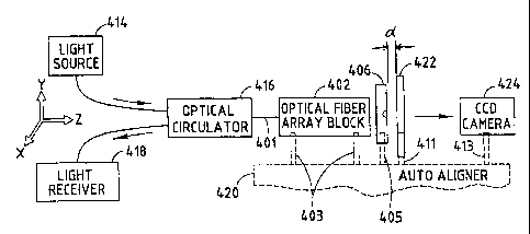
Fig. 4 depicts an alternative system for aligning an optical fiber array block
402
with a microlens array substrate 406. A light source (e.g., a laser diode) 414
is coupled to
an optical circulator 416, which is coupled to a light receiver (e.g., a
photodetector) 418.
The circulator 416 is also coupled to a plurality of optical fibers 401 that
are retained in the
CA 02448945 2010-01-22
6
block 402. The substrate 406 is coupled to the auto-aligner 420 by a fixture
405,
which receives and retains the substrate 406. A half-mirror 422 is coupled to
the auto-
aligner 420 by a fixture 411, which receives and retains the mirror 422. A
charge-
coupled device (CCD) camera 424 is coupled to the auto-aligner 420 through a
fixture
413 that receives and retains the CCD camera 424. In this manner, the auto-
aligner
420 can adjust the block 402, the substrate 406 and the mirror 422 with
respect to the
camera 424 and in relation to each other in three dimensions (X, Y and Z).
Initially, the block 402 and the mirror 422 are brought into contact by the
auto-aligner 420, such that they can be aligned in the OX and OY directions
for
maximum optical power transfer. This puts the block 402 and the mirror 422 in
parallel. Next, the mirror 422 is moved away from the block 402 in the Z
direction.
Then, the substrate 406 is placed between the block 402 and the mirror 422.
The light
source 414 then provides a light beam to at least a first one of the optical
fibers 401
and a last one of the optical fibers 401 such that visual alignment is
conducted by
visually examining the lighting position through the microlens of the
substrate 406
with the camera 424. Next, the mirror 422 and the substrate 406 are positioned
at a
distance a, which corresponds to the optical length between a microlens and a
beam
waist point (the point in the Gaussian beam where the wave front has a
curvature of
zero and the beam diameter is a minimum) to be formed. A light beam is then
inserted
into the fibers 401 and the block 402 and the microlenses of the substrate 406
are
aligned by examining the reflected light power as seen at the light receiver
418. When
optimum alignment is achieved, the block 402 and the substrate 406 are fixed
(e.g.,
with an optical adhesive) to each other to form an arrayed optical fiber
collimator.
FIG. 5 depicts coupling loss as a function of distance for the previously
described procedures. A minimum coupling loss of a pair of collimators aligned
by
the mirror procedure is 0.6 dB, without an anti-reflection (AR) coating on the
microlens surface. As such, coupling loss should be typically less than 0.5 dB
when
the microlens surface is AR coated. It should be noted that the accuracy of
alignment
was improved from between a
CA 02448945 2003-11-28
WO 03/005078 PCT/US02/13582
7
range of about 0.5 to 1 micron to about 0.1 micron in the X and Y axis and
from 0.1 degree
to 0.01 degree in the OX, 6Y and OZ axis alignment.
Moving to Fig. 6, a graph depicting the deviation in alignment as a function
of time
for an optical fiber array block and a microlens array substrate after being
aligned in one
channel is shown. The increase in loss with time is mainly due to thermal
expansion or
shrinkage of the holders and the brackets on the auto-aligner and vibration of
the auto-
aligner. In the process of alignment using a mirror, the mirror and optical
fiber array block
are aligned and parallel at which point they are left for a period of time in
which the mirror
may move to a certain extent during alignment of the substrate and the block.
The
instability of the auto-aligner is generally exhibited by all commercially
available models.
As shown in Fig. 7, another factor that affects the alignment of the
components is
the deviation of the center of rotation of the auto-aligner from the tip of a
first channel
(CH1) and a last channel (CH6) of the block 402 and the surface of the mirror
422. In a
typical auto-aligner, the substrate 406 is fixed and the mirror 422 and the
block 402 are
moved to facilitate alignment. However, when the block 402 and the mirror 422
are
moved, for example, in the 6Y axis, the tip of the first channel and the last
channel, which
are used for alignment points, move not only in 6Y but also in the X and Z
axes. The
mirror 422 moves similarly to the block 402 and while the block 402 can be
automatically
aligned in the X axis, misalignment can remain in the Z axis.
According to another embodiment of the present invention, as is illustrated in
Fig.
8, a dummy block (preferably, an SiO2 or glass block) 826 is utilized in place
of the mirror
422 of Fig. 4. The dummy block 826 is attached to a surface of the substrate
806. As
shown, the optical fiber array block 802 includes a lens spacer 828 that is
coupled (e.g.,
with an optical adhesive) to a surface of the block 802 such that the block
802 and the
spacer 828 form an integrated unit. As such, the block 802 and the spacer 828
are attached
to auto-aligner 820 by a single fixture 803. Likewise, the dummy block 826 is
attached to
the substrate 806, which is coupled to the auto-aligner 820 by a single
fixture 805. A CCD
camera 824 is also coupled to the auto-aligner 820 by a fixture 813. A light
source (e.g., a
laser diode) 814 provides a light beam, through an optical isolator 830, to an
optical
circulator 816. The circulator 816 is coupled to a plurality of optical fibers
801, which are
CA 02448945 2010-01-22
8
retained in the block 802. Preferably, light is inserted into a first optical
fiber of the
fibers 801 and a last optical fiber of the plurality of optical fibers 801 and
the block
802 and the substrate 806 are roughly aligned by visually examining the
lighting
position through the microlenses of the substrate 806 with a CCD camera 824.
The
collimated light beam formed by the microlens of the substrate 806 is
partially
reflected at a surface of the dummy block 826, whose thickness is preferably
adjusted
so that a reflection position corresponds to optical beam center along the
optical axis
of the collimator. The reflected light is reintroduced into the fiber and
directed into a
light receiver (e.g., a photodetector) 818 by the circulator 816. The
alignment of the
block 802 (including the spacer 828) and the substrate 805 (including the
dummy
block 826) is achieved by checking the optical powers of the first channel and
the last
channel. Alternatively, each channel may be examined. In this manner, the
substrate
806 and the block 802 are precisely aligned in all six axes (X, Y, Z, OX, OY
and OZ)
through examining the reflected light power. When proper alignment is
achieved, an
adhesive (e.g., an ultraviolet (UV) optical adhesive) is inserted between a
surface of
the spacer 828 and a surface of the substrate 806 such as to create an
integrated
collimator. A primary advantage of this procedure over the previously
described
procedure is that the number of parts that have to be held on the auto-aligner
decreases from three to two, which allows more precise alignment to be
achieved.
FIG. 9 is a graph illustrating a plurality of curves that define coupling loss
as a
function of spacing for a number of pairs of collimators fabricated using the
setup of
FIG. 8. The minimum coupling loss of a pair of collimators aligned using a
dummy
block was 0.4 dB (Fresnel reflection loss was eliminated, however, connector
loss
was included). It should be noted that the accuracy of alignment was improved
from a
range of about ten to twenty microns to about one micron in the Z axis and
this
procedure is applicable to all six axes.
The previously described procedures are applicable to a wide variety of
collimator
configurations. For example, FIG. 10 depicts an arrayed optical fiber
collimator 1000
that includes a dummy block 1026 that has an angled face to match a sloped
back
surface of a microlens array substrate 1006. Angling the face of the dummy
block
1026 compensates for the slope of the substrate 1006 and provides for more
precise
alignment. As shown in
CA 02448945 2003-11-28
WO 03/005078 PCT/US02/13582
9
Fig. 11, a collimator 1100 with convex or diffractive lenses may include a
dummy block
1126 with a void (e.g., a dent) for alignment. As shown in Fig. 12, when the
collimated
light beam is designed to be at a few degrees deviated from the optical axis
of the
microlenses of a microlens array substrate 1206, a dummy block 1226 with a
slanted back
surface may advantageously be used for more precise alignment. Accordingly, a
number
of procedures have been described herein, which generally reduce the loss of
an arrayed
optical fiber collimator over prior construction techniques.
It will become apparent to those skilled in the art that various modifications
to the
preferred embodiment of the invention as described herein can be made without
departing
from the spirit or scope of the invention as defined by the appended claims.