Note: Descriptions are shown in the official language in which they were submitted.
CA 02449527 2006-04-24
24925-4
BACKGROUND OF INVENTION
The present invention relates to a distributing system for connecting a
line cable or an office cable to patching cords.
There has been proposed a conventional communication system, as
shown in Fig.10A, in which equipments AO to An are mutually connected
to equipments BO to Bn. In order to change connection wiring between the
equipments AO to An and the equipments BO to Bn, a distributing
system 2, as shown in Fig. 10B,
has been employed in which adapters lal to lan and adapters lbl to lbn
are respectively connected to equipments AO to An and equipments BO to
lo Bn. In this case, desired change of connection wiring between the
equipments AO to An and the equipments BO to Bn can be performed by
changing-over with patching cords 31 to 3n between desired pairs of
adapters of a plurality of adapters I provided on plug boards 6 in a
distributing system 2.
Optical cables and metal cables are employed as communication
lines for data communication equipments, while these cables are of single
-core type or multi-core type.
In conventional distributing system, a label recorded with letters,
symbols or bar codes is appended, on each of connector plugs 4al to 4an
and 4b 1 to 4bn connected to two ends of each of patching cords 31 to 3n
coupled to adapters on the distributing system 2, to indicate identification
information ID of the connector plugs.
Connection operation in the distributing system 2 is carried out by
inserting each of the connector plugs 4a1 to 4an and 4b 1 to 4bn connected
to two ends of each of patching cords 31 to 3n to specified one of the
adapters lal to lan and adapters lbl to lbn. Respective ones of the
patching cords are connected between each pair of adapters 1 al to 1 an and
adapters lb 1 to lbn indicated on a wiring table, in the same manner as a
patching cord 31 is connected between the adapter 1 al connected to a
1
CA 02449527 2003-11-14
terminal 01 (not illustrated) of the equipment A0 and the adapter 1 b 1
connected to a terminal 01 (not illustrated) of the equipment A0.
After connection operation is thoroughly fmished, the above
mentioned letters, symbols or bar codes appended on the connector plugs 4
connected to two ends of a patching cord 3 are read out in having a look at
them or by the use of a bar code reader and then applied to a personal
computer (PC) 5 employed as a data processing and display device together
with the address information of the instant connector plug 4.
Correct data representative of connection relationship between each
lo of adapters lal to lan in equipments of one side A and each of adapters
lb1 to 1bn in equipments of another side B are previously stored in the
personal computer 5. Therefore, if erroneous insertion of the connector
plug 4 in the adapter 1 is detected as a result of comparison operations
between connection data of each of the adapters and each of the connector
plugs 4, the questioned connection position is indicated on the display
plane of the PC 5 so that the questioned connection position can be
corrected to a correct connection by changing-over with patching cords
connected to the connector plugs 4.
However, the conventional device has such disadvantages that a
considerable time is necessary for reading out the address information of
the adapter 1 in having a look at them or by the use of a bar code reader,
while miss reading and miss input operation may artificially cause in case
of reading the address information of the adapter 1 and in case of applying
the readout result to the personal computer.
Moreover, since connection operations in the conventional device
are carried out to insert each of the connector plugs connected to two ends
of the patching cord in view of a connection table indicative of a desired
wiring diagram, miss reading of the connection table or miss insertion of
the connection plug may cause, while it is difficult to enhance the operation
2
CA 02449527 2006-04-24
24925-4
efficiency due to necessity of careful wiring operations.
Summary of the invention
An object of an embodiment of the present
invention is to provide a distributing system for enhancing
the operation efficiency of wiring connection working by
automatically reading out address information of adapters or
receptacles and identification information of connector
plugs coupled to the adapters or receptacles.
According to an aspect of the invention, there is
provided a distributing frame for mutually connecting
optical connection lines, comprising: a plurality of
optical connection lines with single or multiple cores,
wherein two ends of each line are provided with connector
plugs, with memory function units capable of untouchably
performing, from the outside of said connectors, writing-in
and reading-out operations of identifying information from
the same connector plugs to which they are respectively
connected; a plurality of plug boards mounted on the
distributing frame; a plurality of optical adapters mounted
separately on the plug boards and connected respectively to
communication lines, for coupling to each of the connector
plugs; a plurality of antennas positioned proximate to each
of the adapters for untouchably performing a writing-in
operation into and reading-out operation of address
information from the memory function unit when each
connector plug is coupled to a desired optical adapter; and
a data processing and display device, connected to a
plurality of said antennas, comprising memory means for
storing a wiring table showing a desired relationship
between the information pertaining to said addresses of said
optical adapters and said information pertaining to
identification of the connector plugs, and display means for
3
CA 02449527 2006-04-24
24925-4
displaying desired parts of said information on the wiring
table; wherein said identification information of each of
the connector plugs coupled to one of said optical adapters
chosen from said desired relationship is displayed on the
display means and stored in the memory means.
There is also provided a distributing frame for
mutually connecting optical connection lines, comprising: a
plurality of optical connection lines with single or
multiple cores, wherein two ends of each line are provided
with connector plugs with memory function units capable of
untouchably performing, from the outside thereof, writing-in
operation and reading-out operation of identification
information of the same connector plugs are respectively
connected; a plurality of plug boards mounted on the
distributing frame; a plurality of receptacles, mounted
separately on the plug boards and connected respectively to
communication lines, for coupling to each of the connector
plugs with memory function units capable of untouchably
performing, from the outside thereof, writing-in operation
and reading-out operations of address information of said
receptacles; a plurality of antennas positioned proximate to
each of the receptacles for untouchably performing a
writing-in operation into and reading-out operation of the
address information from the memory function unit when each
of the connector plugs is coupled to desired one of the
receptacles; and a data processing and display device,
connected to a plurality of said antennas, comprising memory
means for storing a wiring table showing a desired
relationship between said address information of said
receptacles and said identification information of the
connector plugs, and display means for displaying desired
parts of the information on the wiring table; wherein said
identification information of each of the connector plugs
4
CA 02449527 2006-04-24
24925-4
coupled to one of said receptacles specified from said
desired relationship is displayed on the display means and
stored in the memory means.
In the distributing frame, indicators may be
mounted proximate to each of the adapters or the receptacles
in order to be switched ON or OFF in accordance with desired
timing, which switching is controlled by a signal from the
data processing and displaying device.
The distributing frame may further comprise means
for displaying the indicators as two different colors, one
"correct" color and the other a "possibly incorrect" color,
said "possibly incorrect" color being lit precisely at the
point of incorrect connection when considered in light of
the desired relationship between said address information of
said adapters or receptacles and said identification
information of the connector plugs.
BRIEF DESCRIPTION OF THE DRAWINGS
The present invention will be described in details
below with reference to accompanying drawings, in which:
Fig. 1 is a typed view illustrating connection
diagram of an embodiment of a distributing system of the
present invention;
Fig. 2 is a perspective view illustrating a wiring
frame and a plurality of connector adapters employed in the
distributing system of the present invention;
Fig. 3 is a perspective view illustrating examples
of adapters, a patching cord and a data processing and
displaying device employed in the distributing system of the
present invention;
4a
CA 02449527 2006-04-24
24925-4
Fig.4A is a perspective view illustrating an example of an adapter
employed in the distributing system of the present invention;
Fig.4B is a perspective view illustrating another example of an
adapter employed in the distributing system of the present invention;
Fig.5A is a typed side view illustrating an adapter and a connector
plug employed in the distributing system of the present invention;
Fig.5B is another typed side view illustrating an adapter and a
connector plug employed in the distributing system of the present
invention;
Fig.6 is a flow chart explanatory of an example of operating and
processing steps employed in the distributing system of the present
invention;
Fig.7A is a memory map illustrating a collation result in a
processing operation in the distributing system of the present invention;
Fig.7B is a memory map illustrating another collation result in a
processing operation in the distributing system of the present invention;
Fig.8 is a displayed pattern displayed in a processing step in the
distributing system of the present invention;
Fig.9A is a front view illustrating a wiring frame and a plurality of
connector adapters employed in another embodiment of the distributing
system of the present invention;
Fig.9B is a typed connection view illustrating a part of the
embodiment illustrated in Fig. 9A;
Fig.10A is a block diagram illustrating a conventional distributing
system; and
Fig.10B is a block connection diagram illustrating a typed
conventional distributing system.
DETAILED DESCRIPTION OF THE INVENTION
(ENBODIMENT 1)
5
CA 02449527 2006-04-24
2'4925-4
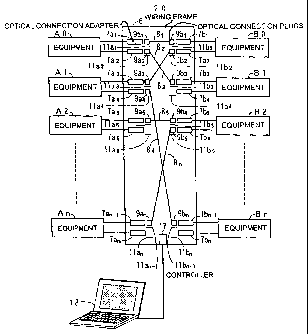
An embodiment of a distributing system 20 of the present invention
will be described with reference to Fig. 1, in which connector adapters and
connector plugs are employed as optical type by way of example. In a
wiring frame 6 for developing the distributing system 20, many optical
connection adapters 7al to 7an and 7b 1 to 7bn are mounted and connected
respectively to equipments A0 to An and BO to Bn. In order to identify
respective one of optical connection plugs 9al to 9an and 9b 1 to 9bn
respectively connected to two ends of the patching cord 81 to 8n as
illustrated in Fig.3 described later, at the neighborhood of the optical
connection adapters 7a1 to 7an and 7b 1 to 7bn, there is provided antennas
llal to llan and libl to llbn each capable of untouchably reading out
identification information ID stored in memory function units 10 which
mounted respectively on the optical connection plugs 9a1 to 9an and 9bl to
9bn.
The optical adapters 7 provided on the wiring frame 6 are arranged,
as illustrated in Fig.2, on plug boards (PB) 12 of No. (01) to No. (n), while
the antennas 11 are connected to a personal computer 18 through a
controller 17 provided in the wiring frame 6.
Fig. 3 illustrates a part of one of the plug boards 12 and a
part of one of the patching cords 8. In this case, four optical
adapters 7 are illustrated on the plug board 12, and the optical
connector plugs 9a and 9b each having a mempry function 10 are
respectively connected to one of the patching cords 8. The rrmerrKDry
function unit 10 on each of the optical connector plugs 9a and 9b is
formed into an outer embeddable coupler 15, as illustrated in
perspective view in Fig. 4. However, the memory function unit 10 can
be fixedly mounted on a body 14 of each optical connector plug 9a
or 9b.
The antenna 11 is mounted near the optical adapter 7, so that mC
memory function unit 10 is positioned just above the antenna 11 capable of
6
CA 02449527 2003-11-14
untouchably reading out the ID information stored in the memory function
unit 10 when the optical connector plug 9a or 9b is insert coupled to the
optical adapter 7. The untouchably reading out technique including the
memory function unit 10 is formed into an integrated circuit of untouchable
type, which has been proposed as an electromagnetic induction system
applied to IC cards and IC fixed-term tickets developed as RFID (Radio
Frequency Information Distributor) systems.
A plurality of the optical adapters 7 is arranged on the plug board
12 formed into an L-shape in the wiring frame 6, and the antennas 11 are
lo positioned, respectively, at the front portions of the optical adapters 7.
Respective ID information symbols designating the respective addresses of
the optical adapters 7 on the wiring frame 6 are assigned to all the optical
adapters 7, so that each of the addresses is designated by the order number
of an instant adapter 7 on a designated one of the plug board 12. These
respective addresses of the optical adapters 7 are previously stored in the
personal computer (PC) 18 employed as a data processing displaying
device.
Fig.5A illustrates a side view of a state preceding from an insertion
of the connector plug 9 to the optical adapter 7 arranged on the plug board
12 formed into an L-shape, while Fig.5B illustrates a side view of an
inserted state of the connector plug 9 to the optical adapter 7.
ID information of the memory function units 10 mounted
respectively on the optical connector plugs 9a and 9b, which are connected
respectively to two ends of the patching cord 8, are usually the same.
However, the 11) information of the memory function units 10 can be
modified to symbols la or lb by way of example.
In a case where the optical connector plugs 9a and 9b connected
respectively to two ends of the patching cord 8 are insert coupled to
designated ones of the optical adapters 7 in view of a wiring diagram, the
7
CA 02449527 2003-11-14
ID information of the memory function unit 10 mounted on the optical
connector plug 9 insert coupled as mentioned above can be read out by the
antenna 11 corresponding to the optical adapter 7 designated from the
personal computer 18. This eliminates essential items in conventional
techniques for inputting, by an operator, the address data of the optical
adapter 7 insert coupled to the connector plug 9a or 9b or the symbol
appended on the connector plug 9a or 9b.
In the distributing system of the present invention, the ID
information of the optical connector plug 9 can be read out from the
lo personal computer 18 in designating the antenna 11 corresponding to the
optical adapter 7 insert coupled to the optical connector plug 9 at each time
when the optical connector plug 9 is insert coupled to the optical adapter 7,
or the ID information of the optical connector plugs 9 insert coupled,
respectively, to the optical adapters 7 can be simultaneously read out in the
order designated from the personal computer 18.
The operations and processing steps in the wiring working of the
distributing system of the present invention will now be described with
reference to a flow chart illustrated in Fig.6. At first, the personal
computer
18 is started in a step S 1. In this starting condition, connection data
2o between communication equipments, that is, the connection data indicative
of connection lines between optical adapters 7a1 to 7an connected to the
equipments of side A and optical adapters 7b 1 to 7bn connected to the
equipments of side B are previously stored in the personal computer 18.
In a next step S2, an operator carries out to insert couple the
connector plugs 9a and 9b of each patching cord 8 to corresponding optical
adapters 7 respectively, and, at each end of the insert coupling operation or
the end of the entire insert coupling operations, the I.D information of the
optical connector plug 9 insert coupled to the optical adapter 7 designated
by the personal computer 18 is read out through the antenna 11 and then
8
CA 02449527 2003-11-14
stored into the address of the instant antenna 11 in an memory of the
personal computer 18. In other words, the ID information data stored in the
memory function 10 of the optical connector plugs 9a and 9b connected,
respectively, to two ends of the patching cord 8 are read out and stored to
respective corresponding addresses of the personal computer 18.
In a step S2, the data read out to the personal computer 18 are
reformed into a memory map of connection relationship illustrated Fig.7A.
In other words, this memory map indicates mutual relationships between
the ID of the memory function units 10 of each optical connector plug 9 to
lo be coupled to respective ones of the antennas 11 and respective address
numbers of the plug boards 12 in the wiring frame 6, and further indicates
mutual relationships between the ID of the memory function units 10 of
each optical connector plug 9 to be coupled to respective ones of the
antennas 11 and respective address numbers of the optical adapters 7.
However, the ID of the memory function units 10 of each optical connector
plug 9 to be coupled to respective ones of the antennas 11 of the optical
adapter 7 are indicated by simple symbols different from that employed in
Fig.l.
In Fig. l, the groups of 7a and 7b of the optical adapters respectively
connected to an equipment group of A0 to An and an equipment group of
BO to Bn are separately illustrated at the right side and the left side.
However, actual positions of the groups of 7a and 7b are optionally
selectable in consideration of the efficiency of wiring.
In a step S3, the memory map illustrated in Fig.7A is rearranged as
illustrated in Fig.7B with reference to the ID of the memory function unit
10 of the optical connector plugs 9. In this case, the ID assigned to each
pair 9a and 9b of connector plugs respectively connected to two ends of
each patching cord 8 indicates that the optical adapter 7 corresponding to
the antenna 11 of No.01 on the plug board 12 of No.01 is connected to the
9
CA 02449527 2003-11-14
optical adapter 7 corresponding to the antenna 11 of No.02 on the plug
board 12 of No.02. As a result of the above identification symbols,
respective connection addresses of two ends of the patching cord 8 can be
confirmed.
In a step 4, instant connection data of communication equipments
after changing wiring are read out from connection data (i.e. data of wiring
map) of respective communication equipments stored in the personal
computer 18.
In a step 5, this instant connection data of communication
lo equipments after changing wiring is collated with the ID data read out from
the personal computer 18 in the step S2.
In a step 6, if the above collation operation indicates any erroneous
wiring position due to non-coincidence, this erroneous wiring position is
indicated on a display plane of the personal computer 18 to correct the
erroneous wiring.
The erroneous wiring is corrected in accordance with the above
indication on a display of the personal computer 18 (S7), and the ID of the
connector plug 9 of the corrected wiring position is read out (S8). When all
the insertion coupling of the connector plugs 9 are correctly performed in
coincidence states in the step S5, the operation is shifted to a step S9 of
indication, in which a data table shown in Fig. 8 is displayed on the display
plane of the personal computer 18 in accordance with connection data
shown in Fig.7B. After the step S9, the operation reaches the end (S 10).
In the distributing system 20 of the present invention, when an
operator inserts, in view of the wiring table, each of the optical connector
plugs 9 connected respectively to two ends of the patching cord 8 to a
specified one of the optical adapter, ID data of the connector plugs 9
inserted are read out at each insertion time or simultaneously after fmishing
insertion operations of a necessary number of the connector plugs 9 in
CA 02449527 2003-11-14
order to be able to judge whether each insertion coupling is correct or not.
This eliminate necessity in conventional techniques for watching with the
eye the insertion state of the connector plugs 9 or for reading out by a
bar-cord reader any ID information of the connector plugs 9. Therefore, the
distributing system 20 of the present invention has merits that reliability
and operation efficiency of wiring operation can be enhanced without
erroneous reading out respective connection data or erroneous inputting of
respective connection data to the personal computer.
LEMBODIlVIENT 2)
With reference to Figs.9A and 9B, another embodiments of the
present invention will be described, in which an indicator is provided at the
neighborhood of each of the optical connection adapters 7. In this case,
Fig.9A illustrates a front view of the wiring frame 6, and Fig.9B is a typical
view of a part of the plug board 12 provided on the wiring frame 6, on
which the antennas 11 and the indicators 19 are mounted in pairs. The
indicators 19 are mounted at the lower surface of the plug board 12, by way
of example, on the upper surface side of which each optical adapters 7 are
mounted, and further connected through each one of controllers 17 to the
personal computer 18. In the above construction, the indicators 19 are
successively lightened in green color, for exam.ple, in accordance with
corrected connection data (i.e. wiring map) of communication equipments
stored in the personal computer 18 in order to indicate the operator each
position of the optical adapter 7, to which each of the optical connector
plugs 9 connected respectively to two ends of the patching cord 8 are
26 inserted.
The indicators 19 are ON-OFF switched under control of a control
signal, which is read out from the personal computer 18 in a switching
timing as mentioned below and held in a corresponding one of the
controllers 17. To this end, respective indicators 19 of two optical adapters
11
CA 02449527 2006-04-24
24925-4
7 to be mutually connected are simultaneously lightened to insert
respective connector plugs 9 of the patching cord 8 into the two optical
adapters 7 lightened. When the two optical adapters 7 are mutually
connected by the patching cord 8, the respective indicators 19 of the two
optical adapters 7 already connected is switched to the OFF state.
Thereafter, respective indicators 19 of two optical adapters 7 to be next
mutually connected are simultaneously lightened to guide to insert
respective connector plugs 9 of the next patching cord 8 into the two
optical adapters 7 lightened. In these operations, each insertion of the
optical connection plugs 9 to the optical adapter 7 is detected by the use of
the antenna 11 as mentioned previously.
The indicators 19 can be lit up in two different colors--green and red, for
example-- such that if an incorrect insertion is detected between the
insertion of the
optical connector plug 9 of the patching cord 8 into the optical adapter 7 and
the correct.
connection data (i.e., wiring map) of the entire communication equipment
cannot take
place, a control signal indicating this incorrect insertion will be sent from
the *personal
computer 18 and the questionable position of the optical adapter 7, positioned
as it is at
the incorrect connection; will be indicated by a lit-up red LED.
Since the embodiment 2 of the present invention is so constructed
that the optical adapters 7 to be coupled to the optical connector plugs 9 of
the patching cord 8 are successively indicated by the indicators 19, this
embodiment 2 of the present invention has merits, such as non-necessity of
reading out operation by the operator and enhancement of the operation
efficiency and reliability of the connection working.
The above are mainly described with referenm to mutual
connection between a single core optical connector plug and an optical
adapter. However, the present invention can be also applied to mutual
connection between a metal connector plug and a metal receptacle, and
12
CA 02449527 2003-11-14
mutual connection between a multi-core connector plug and an adapter or
receptacle.
As mentioned above, the distributing system of the present
invention possesses the following characteristic features:
(1) The Connector plugs with memory function units capable of
untouchably reading out ID stored therein are connected to two ends of the
patching cord, which is employed for connecting between desired two
adapters of a plurality of adapters mounted in the distributing system.
(2) Antennas capable of untouchably reading out the ID stored in
lo the memory function units are positioned at the neighborhood of each of
the adapters.
(3) When each one of the connector plugs with memory function
units is inserted to a desired one of the adapters, connection data relating
to
the ID of the connector plug connected is automatically applied to a data
processing and displaying device to display the connection data processed
on the displaying device, thereby enhancing the operation efficiency and
reliability of the connection working.
(4) Each of indicators are mounted at the neighborhood of each of
the adapters in order to be ON-OFF switched in accordance with desired
switching timing, which is controlled by a control signal from the data
processing and displaying device. Therefore, connection operation of the
connector plugs of a patching cord can be correctly and swiftly perfonned
to effectively enhancing the operation efficiency and reliability of the
connection working.
13