Note: Descriptions are shown in the official language in which they were submitted.
CA 02451283 2003-11-27
ELECTRONIC SWITCH AND METHOD OF USE FOR
ACTUATING A DOOR
FIELD OF THE INVENTION
The present invention relates to an electronic switch using a pressure
transducer for actuation thereof, and more particularly relates to a method of
using an
electronic switch for actuating a door.
BACKGROUND
Due to the material wear resulting in limited number of on and off cycles
typically associated with mechanical switches, the use of electronic switching
circuits
and electronic switches are known to be desirable for their extended life. US
patents
5,231,326 to Echols and 5,170,087 to Karr disclose examples of switches
including
pressure transducers in a switch in which minimal wear of the components
results. A
complex circuitry is required in each instance however as the signal from the
pressure
transducer is required to be fed to a transistor amplifier requiring a power
supply for
powering related switching circuitry. The resulting circuitry is complex and
costly to
manufacture and implement.
In one example of an application for a switch, wall mounted svvitches are
known for actuating powered doors for access in various public buildings and
the like
for disabled persons. The switches in this instance are often subjected to
considerable abuse due to their public environment and accordingly a switch
involving
minimal wear is desired. Known switches for this application however typically
require
mechanical components or complex circuitry in order to actuate opening of the
door.
Vandalising of the complex components of the switch results in further cost
for
maintenance of such known designs of switches.
SUMMARY
According to one aspect of the present invention there is provided a
CA 02451283 2003-11-27
-2-
switch comprising:
a pair of switch terminals;
a transistor having a drain terminal and a source terminal connecting the
transistor in series between the switch terminals whereby current flow is
permitted
between the switch terminals when the transistor is closed;
a housing having a movable contact area; and
a pressure transducer located within the housing in communication with
the contact area;
the transistor including a gate terminal connected to the pressure
transducer to close the transistor when pressure is applied to the pressure
transducer.
The direct connection of the transducer to the gate of the transistor and
providing that the transistor is directly coupled in series with the switch
terminals
provides a simple construction which can be readily manufactured and in which
the
switching components do not require external power for operation thereof. The
voltage difference provided by the pressure transducer is sufficient to
operate the
transistor when coupled in the above configuration.
According to a second aspect of the present invention there is provided
a switch comprising:
a pair of switch terminals;
a transistor having a drain terminal and a source terminal connecting the
transistor between the switch terminals whereby current flow is permitted
between the
switch terminals when the transistor is closed;
a housing including a mounting plate for mounting on a suitable
supporting surface and a cover plate supported on the mounting plate for
relative
movement therebetween; and
a pressure transducer located between the mounting plate and the
CA 02451283 2003-11-27
-3-
cover plate of the housing;
the transistor including a gate terminal connected to the pressure
transducer to close the transistor when pressure is applied to the pressure
transducer;
the cover plate including a plurality of retainer members selectively
received in co-operating slots in the mounting plate, accessible through a
rear of the
mounting plate such that access to the slots is blocked to retain the cover
plate on the
mounting plate when the mounting plate is mounted on a supporting surface.
The arrangement of a housing in which a cover plate is provided for
concealing electronic components of the switch and in which access to remove
the
cover is restricted once the mounting plate is in a secure mounted positionY
minimizes
the opportunity for vandalising or excessive wear of the components of the
switch.
According to a further aspect of the present invention there is provided a
method of actuating an automatic door, the method comprising:
providing a door actuator to open the door responsive to condition of a
door switching circuit;
providing a door switch comprising a pressure transducer and a
transistor having a drain terminal, a source terminal and a gate terminal
connected to
the pressure transducer;
connecting the drain terminal and the source terminal in series with the
door switching circuit; and
applying pressure to the pressure transducer to close the transistor and
actuate the door actuator via the door switching circuit.
The transistor in each instance preferably comprises a TMOS power
transistor in which the gate terminal comprises a capacitor. Accordingly there
may be
provided a bleed-off resistor coupled to the gate terminal to prevent
erroneous
charges accumulating on the gate.
CA 02451283 2003-11-27
-4-
When the transistors comprise TMOS power transistors, preferably a
pair of the transistors connected at respective source and drain terminals in
an anti-
serial configuration with the switch terminals for proper operation in
alternating current
applications.
There may be provided a pair of voltage limiting diodes coupled together
in an opposed configuration in parallel with the pair of transistors between
the switch
terminals to limit maximum voltage applied across the transistors.
A voltage limiting diode is preferably coupled between the gate terminal
and the source terminal of the transistors to limit maximum voltage applied to
the gate
terminal.
The housing may include a mounting plate for mounting on a suitable
supporting surface in which the movable contact area comprises a cover plate
supported on the mounting plate for relative movement therebetween. A stop or
limit
may be formed on the housing to limit maximum deflection of the cover plate
relative
to the mounting plate.
When the mounting plate includes mounting apertures formed therein
for receiving fasteners to mount the mounting plate to a supporting surface,
the cover
plate preferably conceals the mounting apertures when supported on the
mounting
plate.
The cover plate may include a plurality of retainer members selectively
received in co-operating slots in the mounting plate accessible through a rear
of the
mounting plate such that access to the slots is blocked to retain the cover
plate on the
mounting plate when the mounting plate is mounted on a supporting surface.
The retainer members preferably each comprise a hook having a free
end portion which is flat lying generally parallel to a front surface of the
cover plate for
ease of sliding behind the mounting plate during assembly.
CA 02451283 2003-11-27
-5-
The retainer members preferably comprise hooks which are provided on
opposing sides of the cover portion to confront one another.
BRIEF DESCRIPTION OF THE DRAWINGS
In the accompanying drawings, which illustrate an exemplary
embodiment of the present invention:
Figure 1 is schematic view of the components of the switch in
connection with a door actuating circuit.
Figure 2 is a circuit diagram of the switch.
Figure 3 is a perspective view of the housing locating the electronic
assembly of the switch therein.
Figures 4A and 4B are side elevational views of the switch in respective
closed and open positions.
Figures 5A through 5E are side elevational views of the cover as it is
mounted into place on the mounting plate.
DETAILED DESCRIPTION
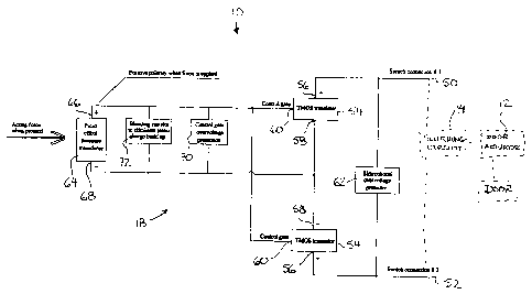
Referring to the accompanying drawings, there is illustrated an
electronic switch generally indicated by reference numeral 10. The switch 10
is
particularly suited for closing a switching circuit to actuate any one of
several known
devices. In the illustrated example a door can be opened by a door actuator 12
by
means of a door switching circuit 14 which is closed by a wall mounted version
of the
door switch 10.
The switch 10 includes a housing 16 which houses and protects an
electronic assembly 18 therein. The housing includes a mounting plate 20 and a
cover plate 22 which can be supported on the mounting plate for relative
movement
therebetween. The mounting plate 20 is a flat rectangular plate including a
pair of
mounting apertures 24 formed therein at opposing ends of the plate such that
the
CA 02451283 2003-11-27
-6-
plate is securable flat against a wall or other supporting surface 26. The
mounting
apertures 24 include a large aperture portion for receiving the head of a
fastener
therethrough and a slot portion in a keyhole shape to slidably receive the
shaft of a
fastener therethrough while retaining the head of the fastener thereon.
The mounting plate 20 includes two pairs of upright mounting flanges 28
spaced apart from one another on opposing sides 30 of the mounting plate
respectively and extend upward from the top side 31. Each mounting flange
includes
a wide retaining slot 32 formed therein which extends from a rear side 33 of
the plate
to terminate centrally within the mounting flange 28 spaced from the free end
of the
flange. The retaining slot 32 also extends inwardly into the mounting plate to
provide
access to the retaining slot from the rear of the mounting plate. An access
slot 34 is
provided adjacent each mounting flange at equal spacings from respective
retaining
slots 32. Each access slot 34 is offset from the respective retaining slot 32
in the
same direction towards the top end of the plate along respective sides 30 of
the plate.
Each access slot extends inwardly the same depth and width as the retaining
slots 32
extend into the plate.
The cover plate 22 is rectangular and flat in the illustrated embodiment,
having similar dimensions as the mounting plate 20. A pair of retainer members
36
are provided at spaced positions along each of two opposing sides 38 of the
cover
plate so as to be aligned with the retaining slots 32 when the cover plate and
mounting plate are aligned. Each retainer member 36 comprises a hook with a
depending flange 40 projecting perpendicularly to a cover surface 42 of the
cover
plate and a hook flange 44 lying parallel to the cover surface 42. The hook
flanges 44
are wide and flat and project inwardly so as to confront one another, while
being
suitably sized to be received within the retaining slots 32. The depending
flange 40 is
longer than the respective mounting flanges 28 such that the hook flanges 44
are
~.,.~.,~:,-.-"~.::....~.~" ,.,..,~-",....~,~.~.-.,R.,...a.m~,ac. .~,.,.~ri
=~~....:~a~:ss~~:s~.,.~;_.~,N~,e,:~,.",.~R-~;;,: ~r~.,~
~saru..vp~.,~,~za~.w...,~:~,.,~r=,.,~.".~...~.,_-_~._...__..__ ..
CA 02451283 2003-11-27
_
sufficiently spaced from the cover surFace 42 of the cover plate that the
mounting
plate can be received slidably between the opposing pairs of retainer members
36
between the hook flanges 44 and the cover surface 42.
Before installation of the switch on a wall or other supporting surface,
the housing is first assembled, typically at the factory where it is
manufactured. In
order to assemble the housing, the cover plate is attached to the mounting
plate by
following the steps illustrated in Figures 5A through 5E. Accordingly, the
retainer
members follow a path as illustrated sequentially by reference characters A,
B, C and
D in Figure 3 so as to first pass through the access slot 34 from the front
side 31 to
the rear side 33 of the mounting plate to be subsequently received in the
respective
retaining slot.
The cover plate is first displaced such that the retainer members are
aligned with the access slots 34 in the mounting plate as in Figure 5B. As the
mounting plate and cover plate are brought together in Figure 5C, the hook
flanges
are received through the respective access slots to be located rearwardly of
the
mounting plate. Longitudinal sliding movement of the mounting plate and cover
plate
are then permitted relative to one another.
From the position of Figure 5C, the cover plate is slid with the hook
flanges 44 along the rear side 33 of the mounting plate, as in Figure 5D,
until the hook
flanges align with the retaining slots formed in the upright flanges of the
mounting
plate, shown in Figure 5E. Pulling the cover plate and mounting plate apart
from one
another, from the position of Figure 5E, results in the retainer members being
fully
retained within the retaining slots once access through the rear side 33 of
the
mounting plate is blocked as occurs when the switch is installed on a
supporting
surface as described further below.
The mounting plate, and cover plate supported thereon, are attached to
CA 02451283 2003-11-27
a supporting surface using suitable fasteners which are first secured to the
supporting
surface. The mounting plate is first attached with the fasteners not fully
tightened so
that sufficient space is provided between heads of the fasteners and the
supporting
surface to receive the thickness of the mounting plate.
The keyhole shape of the mounting apertures 24 in the mounting plate,
as described above, permits the heads of the fasteners to be inserted in the
mounting
apertures through the larger portion to be subsequently received in the slot
portion by
longitudinal sliding movement of the mounting plate relative to the wall and
fasteners.
The fasteners preferably comprise a threaded type fastener having a head which
is
polygonal in cross section for gripping with a suitable wrench and the like.
Further tightening of the fasteners by inserting a wrench at respective
ends of the housing between the mounting plate and cover plate permits the
mounting
plate to be securely tightened directly adjacent the wall. The supporting
surface,
forming the wall, blocks access to the retaining slots 32 by blocking the
rear' surface of
the mounting plate once the fasteners are fully tightened and the slot portion
of the
mounting apertures are gripped between the heads of the fasteners and the
supporting surface.
The electronic assembly 18 is supported centrally between the plates.
The assembly includes first and second switch terminals 50 and 52
respectively. The
switch terminals 50 and 52 are connected in series in a switching circuit for
opening
and closing the circuit. Current between the switching terminals is allowed in
both
directions when the condition of the switch is closed while current between
the
terminals is interrupted in both directions in the open condition.
The switch includes two TMOS power transistors 54 which are coupled
in an anti-serial configuration between the switch terminals 50 and 52. Each
transistor 54 includes a drain terminal 56 a source terminal 58 and a gate
terminal 60.
_r. ....
CA 02451283 2003-11-27
_g_
The gate terminal 60 comprises a capacitor which controls the current flow
properties
between the drain and source terminals when a positive voltage is applied to
the
capacitor forming the gate terminal 60. The TMDS power transistor 54 permits
uninterrupted current in one direction in the open condition of the transistor
between
the drain and source terminals. When the transistor is in a closed condition,
a closed
circuit is formed between the drain and source terminals. In the opposite
direction of
the flow, the transistor acts as a diode.
In the anti-serial configuration, each of the transistors is connected at
the respective drain and source terminals between the switch terminals 50 and
52 in
series with one another but in an opposed configuration such that both the
source
terminals are directly connected to each other while the drain terminals 56
are
connected to the switch terminals respectively. By providing two transistors
in anti-
serial configuration the switch is effective in alternating current
applications as the
current is effectively interrupted in both directions due to each transistor
acting as a
diode limiting current in opposite directions when the transistors are in the
open
condition. In the closed condition of the transistors current flow is
permitted in either
direction across the transistors to effectively close the switch.
Parallel to the transistors and in series between the switch terminals, a
pair of confronting voltage limiting diodes 62 are provided which act to limit
voltage
applied across the transistor's. The pair of diodes 62 are mounted in series
with one
another in opposed orientation between the drain terminals of the transistors.
A pressure transducer 64 is provided between the mounting plate and
the cover plate to actively close the transistors. The pressure transducer
includes a
positive terminal 66 connected to both of the gate terminals 60 of the
transistors and a
negative terminal 68 connected to both of the source terminals of the
transistors.
Applying pressure to the pressure transducer causes a positive voltage to be
applied
CA 02451283 2003-11-27
-10-
to the gates of the transistors relative to the source terminals by piezo
effect.
Coupled in parallel with the transducer between the gate and source
terminals of the transistors is a voltage limiting diode 70 which protects the
gates from
an aver voltage. Also in parallel with the transducer between the gate and
source
terminals of the transistor are a pair of bleed off resistors in series with
one another.
The resistors 72 prevent accumulation of a positive charge at the capacitor of
the gate
terminals so as to prevent erroneous activation of the transistors resulting
from static
charge build-ups or charges resulting from temperature variation of the
pressure
transducer and surrounding housing which may apply a stress or pressure on the
transducer.
In use, pressure is applied to the cover plate in which the surface
thereof comprises a contact area of the switch. The contact area of the cover
is
movable with the cover relative to the mounting plate so that pressure is
applied to the
transducer when the contact area is pressed. The pressure transducer causes
voltage to be applied to the gate terminal by piezo effect to close the
transistors which
thus closes the switch to actuate the switching circuit and door actuator to
open the
door. The length of the retainer members of the cover plate are selected so
that the
retainer members abut the supporting surface upan which the mounting plate is
mounted when a maximum recommended depression of the pressure transducer is
reached to limit further deflection or deformation of the transducer which
might
otherwise cause damage. In an alternative form, limiting of movement between
the
cover plate and the mounting plate may be accomplished by any suitable stop
member formed therebetween.
As noted above with regard to mounting of the cover plate onto the
mounting plate, the cover plate travels through the path A-B-C-D to interlock
with
mounting plate. Once the two plates are interlocked, springs (not shown at the
a
CA 02451283 2003-11-27
-11-
picture) keep the plates apart preventing thus accidental disengagement. By
attaching
the bottom part to a surface like door jamb, the A-B-C-D path is interrupted
between
points B and C and the switch can not be disassembled, once installed. Once
installed the cover plate, if depressed, moves relative to the mounting plate
and exerts
defined pressure on pressure transducer. The transducer generates voltage used
in
turn to change conductivity of a solid state switch.
The number of tabs and slots to interlock is not limited to this particular
arrangement, as it may be any number of these, to yield the same result. What
is
important is the fact that certain points must travel on a particular path
which is
interrupted once the assembly is attached to a surface, preventing thus any
possibility
for disassembly.
The purpose of this interlocking mechanism is to provide means as to
assembleJdisassemble the switch without a need for any tools or any material
displacement, like bending or forming. This further facilitates easy
inspection,
cleaning, repair or replacement of any damaged part.
Apart from the unique mechanical way the switch is assembled, the
actual switching is accomplished by electronic means, so that there is no
material
wear or resulting limited number of ONIOFF cycles as is typically associated
with
mechanical door access switches. The switching utilizes two TMOS transistors
in anti-
serial configuration, with their gate terminals connected together. To change
the state
of a TMOS transistor from nonconductive to conductive, the control electrode,
the
gate terminal, has to have certain potential relative to the common electrode
called
the source terminal. Depending on the TMOS transistor construction this
potential is
typically +/-3 to +J-8 volts. An important property of the gate terminal is
that no current
is needed to maintain the TMOS transistor in its ON state, as the gate
terminal is
basically a capacitor, therefore only potential is needed to change the
conductivity.
CA 02451283 2003-11-27
-12-
This potential is generated by the pressure transducer utilizing the piezo
effect. In
addition to the above, the actual circuit has high value bleedoff resistor
between the
gate and source terminals to prevent any static electricity build up. Also a
Zener
diode limits the maximum gate voltage to such a value as to not exceed the
TMOS
transistor specifications.
While one embodiment of the present invention has been described in
the foregoing, it is to be understood that other embodiments are possible
within the
scope of the invention. For example, the cover plate may be of various shapes
including circular profiles or plates having a curved or canvex surface in
which size of
the plate is preferably equal to or greater than the mounting plate for
concealing the
mounting plate or at least the fasteners thereof. The invention is to be
considered
limited solely by the scope of the appended claims.