Note: Descriptions are shown in the official language in which they were submitted.
CA 02451636 2003-12-22
WO 03/003381 PCT/USO1/20575
LdW TEMPERATURE METHOD AND COMPOSITIONS FOR PRODUCING
ELECTRICAL CONDUCTORS
Background of the Invention
1. Field of the Invention
The present invention relates to compositions which can be used to apply
conductors to electronic components such as printed circuit boards and
semiconductors,
particularly, to compositions which can be applied and converted to solid
conductors at
temperatures below 450°C.
2. Related Art
A common method for printed circuit fabrication process is subtractive or semi-
additive processes in which conductors are formed by etching away unwanted
copper. A
fully additive process would have many advantages over the subtractive or semi-
additive
methods. The primary problem in providing a wholly additive process for
producing
printed circuitry is the requirement for high electrical conductivity with low
enough
curing temperature to be compatible with polymer-based circuit boards. Another
major
problem is making connections to the additive traces, preferably by
conventional
soldering. Present technology includes low cure temperature conductive epoxies
and
transient liquid phase materials which produce traces with poor electrical
conductivity
and poor solderability or high temperature thick film inks which produce
traces with good
electrical conductivity and good solderability but which are limited to
ceramic substrates.
These small, expensive and specialized substrates are required to withstand
the thick film
ink firing temperatures of more than 650°C and usually above
850°C . A method which
could duplicate the performance of thick film inks but on polymer-based
substrates at 250
to 350°C would permit broad, worldwide application of this technology
in the $27 billion
rigid circuit board industry and the $2.5 billion flexible circuit industry.
CA 02451636 2003-12-22
WO 03/003381 PCT/USO1/20575
"Thick film" technology is routinely practiced to produce hybrid circuits on
ceramic substrates. R. W. Vest, "Electronic Ceramics", R. Breckenridge, ed.,
1991. The
conductor patterns are created by silk screening or stencil printing thick
film pastes or
inks onto ceramic substrates and firing them at temperatures of 850 to
1100°C to reduce
the metal-containing inks to metal. An example of such inks are silver-
palladium
compositions which have recently been reviewed by Wang, Dougherty, Huebner and
Pepin, J. Am. Ceram. Soc. 77(12), 3051-72 (1994). Typically thick film inks
contain
metal powders, an inorganic glass binder and a vehicle consisting of a polymer
binder
and a solvent. The vehicle provides the correct consistency for screen
printing and
consists typically of a polymer such as ethyl cellulose, hydrogenated rosin or
polyacrylics
dissolved in a low volatility solvent. Common solvents are terpineol, dibutyl
carbitol and
various glycol ethers and esters. The inks are applied to ceramic substrates
by screen
printing, dried to drive off the solvent and heat treated, usually in a belt
furnace, to
decompose the polymer binder and fuse the metal and the inorganic glass
binder. The
glass phase provides the bond to the substrate which is usually alumina, and
the metal
provides the electrical conductivity. Typically the conductors have a striated
cross section
with layers of glass alternating with layers of metal. The glass tends to
concentrate at the
ceramic interface and the metal at the air interface. The conductivity is
typically one half
to one quarter that of the bulk metal.
A number of thick film compositions contain surfactants to improve
screenability
and stability of the metal powder dispersions. Often these surfactants are
metallo-organic
compounds such as soaps of carboxylic acids. These are convenient in that they
will
decompose at relatively low temperature to deposit the metal or its oxide
which can
perform a useful function in the fired conductor.
LT.S. Patents 5,071,826 issued on Dec. 10, 1991 and 5,338,507 issued on Aug.
16, 1994 to J.T. Anderson, V. K. Nagesdh and R.C. Ruby, disclose the addition
of silver
neodecanoate to superconducting oxide mixtures in which the neodecanoate is
decomposed to the metal at 300°C to coat the superconducting grains
with silver. The
coated grains are then sintered and oxidized at 600-800°C to produce an
oxide
superconductor of enhanced strength and critical current.
2
CA 02451636 2003-12-22
WO 03/003381 PCT/USO1/20575
'The addition of titanate to thick film conductors by decomposition of an
organo-
metallic titanate is described by K. M. Nair in U.S. Patent 4,381,945 issued
on May 3,
1983.
U.S. Patent 4,599,277 issued on Jul. 8, 1986 to J. M. Brownlow discloses
adding
organo-metallic compounds to thick film inks to increase the densification
temperature of
the metal to match that of the ceramic substrate at 850-950°C , the
inverse of.the process
required to apply conductors to polymer circuits at low temperatures.
Conventional thick film paste compositions containing silver flake, glass frit
and
silver resinates, which are carboxylic acid soaps, as well as surfactants such
as Triton X
100, were described in U.S. Patents 5,075,262, issued on Dec. 24, 1991 and 5,
183,784,
issued on Feb. 2, 1993 to M.N. Nguyen and coworkers. The objective was to
eliminate the
preliminary drying step after printing, and the resinate was said to promote
adhesion and
minimize cracks and voids in bonding semiconductor dies to a ceramic substrate
at 350-
450°C . V. K. Nagesh and R. M. Fulrath were issued U.S. Patent
4,130,671 on Dec. 19,
1978. It discloses a similar composition of glass frit and silver resinate
which was
decomposed at low temperature to provide silver-coated glass particles similar
to the
superconductor of Anderson above. The particles were applied to a substrate
either before
or after decomposition of the resinate and fired in an oxidizing atmosphere at
500 to
700°C to provide a conductor of metal-coated glass particles.
~ Still other conventional thick film compositions of glass and metal powders
in an
organic vehicle but without the resinate are described in U.S. Patents
5,250,229 and
5,378,408
To create a low temperature analog of the thick film process, it will be
necessary
to find a new mechanism to obtain adhesion and cohesion of the deposited metal
which
can operate at temperatures below 450°C , which is the extreme upper
temperature limit
that most polymers can tolerate. The use of inorganic glass powder binders
which are
universally used in conventional thick film inks is not possible in this
application because
none of them melt a low enough temperature, and the glass will not bond to the
metal or
to the polymer substrates.
Other approaches to this objective have been described. The most common one is
the creation of electrically conductive inks or pastes by incorporating metal
powder,
3
CA 02451636 2003-12-22
WO 03/003381 PCT/USO1/20575
usually silver powder, in an organic matrix, the so-called "Polymer Thick
Filin "
materials. This is a major industry with products available from Ablestik,
AIT, Hokurika,
M-Tech, Thermoset, Epoxy Technology and Ferro, among others. These materials
can be
printed on circuit boards, and they have good adhesion. An example of the
application of
this technology was described in an article by K. Dreyfack in Electronics
52(17), 2E-4E ,
1979, on Societie des Produits Industrielles ITT's silk screening silver and
graphite-based
conductors of this type onto rigid and flexible circuits. One problem with
this approach is
that the inks conduct by random contacts between powder grains in the organic
matrix,
and the conductivity is poor. Typical values of the resistivity, which is the
reciprocal of
conductivity, are 40 to 60 microohm cm, compared to bulk silver at 1.59
microohm cm
and high temperature thick film conductors at 3-6 microohm cm. Still snore
disturbing is
the fact that the electrical conductivity is not constant with time. The
conductivity
depends on adventitious contacts between individual metal grains which are
prone to be
made and broken randomly as the trace is heated and cooled, and particularly
as it is
exposed to moisture and other environmental influences. Another major problem
with
polymer thick film materials is that because of their organic content, they
are not
solderable.
A typical resin-bonded copper powder conductor is described in Japanese Patent
Application 52-68507, June, 1977. U.S. Patent 4,775,439 issued on Oct. 4, 1988
to R.E.
Seeger and N.H. Morgan, describes a more elaborate polymer thick film
approach. In this
concept metal powder and binder are applied to a substrate and dried. The
trace is then
covered by a polymer film which is adhesively laminated to the substrate to
hold the
conductor in place. This does not address the problem of obtaining electrical
conductivity
comparable to bulk metal.
Bulk conductivity has been achieved at low temperature by decomposing metallo-
organic compounds on various substrates. They can be applied by ink j et
printing as
described by R. W. Vest, E. P. Tweedell and R. C. Buchanan, Int. J. of Hybrid
Microelectronics _6, 261-267, 1983. Vest et al have investigated so-called MOD
(Metallo-
Organic Decomposition) technology over many years. The most relevant aspect of
this
research was reviewed in "Liquid Ink Jet Printing with MOD Inks for Hybrid
Microcircuits" Teng, K.F., and Vest, R.W., IEEE Transactions on Components,
Hybrids
4
CA 02451636 2003-12-22
WO 03/003381 PCT/USO1/20575
and Manufacturing Technology,12(4), 545-549, 1987. The authors described their
work
on printing silver and gold conductors as well as dielectrics and resistors.
MOD
compounds are pure synthetic metallo-organic compounds which decompose cleanly
at
low temperature to precipitate the metal as the metallic element or the oxide,
depending
on the metal and the atmosphere. The noble metals, silver, gold and the
platinum group
decompose to metal films in air. The organic moiety is bonded to the metal
through a
hetero-atom providing a weak link that provides for easy decomposition at low
temperature. An oxygen bond, as in carboxylic acid-metal soaps, has been found
to be
satisfactory, as have amine bonds for gold and platinum.
Vest et al investigated metallization of ceramic substrates and silicon by ink
jet
printing of xylene solutions of soaps such as silver neodecanoate and gold
amine 2-
ethylhexanoate. Images of satisfactory resolution (0.003 inches or 75 microns)
were
obtained, but the conductivity was low because of the extremely small
thickness of the
layers after decomposition which was less than a micron. Preliminary
experiments by
Partnerships Limited on epoxy-glass circuit boards with silver neodecanoate
solutions
demonstrated that well-bonded conductors could be produced on polymer
substrates.
Again, the difficulty was that they were very thin and had inadequate
conductivity. It was
found that the addition of more MOD compound resulted in wider traces but not
thicker
ones. The MOD compound melts before decomposing and spreads over the surface
uncontrollably. Since melting provides for a well-consolidated metal deposit
after
decomposition, which is desirable, and since some MOD compounds are actually
liquids
at room temperature, this is an unavoidable problem. A possible solution to
this problem
is to build up the thickness by printing many layers, which Vest et al found
suitable for
metallizing silicon solar cells, but this detracts from the single pass
production of circuits,
which is our objective.
Similar materials and techniques have been used to apply thin film
metallization
and seed coatings which are then built up with solder or electroplating. U.S.
Patent
4,650,108, issued on Mar. 17, 1987, to B. D. Gallegher; U.S. Patent 4,808,274
issued on
Feb. 28, 1989, to P. H. Nguyen; U.S. Patent 5,059,242 issued on Oct. 22, 1991
to M. G.
Firmstone and A. Lindley and U. S. Patent 5,173,330 issued on Dec. 22, 1992,
to T.
5
CA 02451636 2003-12-22
WO 03/003381 PCT/USO1/20575
Asano, S. Mizuguclu and T. Isikawa, are examples. Thin films alone cannot
provide
adequate conductivity.
A creative attempt to circumvent the resistivity problem was described in U.S.
Patent 4,487,811 issued on Dec. 11, 1984, to C.W. Eichelberger. The patent
describes
augmenting the conductivity by a replacement reaction of metal in the deposit
by a more
noble metal in solution, for example the replacement of iron by copper. In the
process of
doing this, the contact between particles is improved by the greater volume of
the
replacement metal and its greater intrinsic conductivity. A resistivity of 7.5
microohln cm
was achieved, substantially better than silver-loaded epoxies, but short of
the performance
of thick film inks.
The replacement reaction solved yet another problem of polymer inks in that
the
material was solderable, which conductive epoxy formulations in general are
not. Another
approach to solderability was described in U.S. Patent 4,548,879 issued on
Oct. 22, 1985
to F. St. John and W. Martin. Nickel powder was coated with saturated
monocarboxylic
acid with ten or more carbon atoms. The coated powder was mixed with novolac
epoxy
resins in a butyl carbitol acetate vehicle and silk screened onto an epoxy-
glass board.
After curing at 165°C, the conductive trace could be solder-coated by
fluxing and dipping
into molten solder, while a trace made with uncoated nickel powder could not
be
soldered. No improvement in electrical conductivity was described with this
process.
A silver powder is disclosed in "Novel Silver Powder Composition", U.S. Patent
4,186,244 issued Jan. 29, 1980, and "Process for Forming Novel Silver Powder
Composition", U.S. Patent 4,463,030 issued July, 31, 1984, Both issued to R.
J.
Deffeyes, and H. W. Armstrong. The silver powder was formed by decomposing dry
silver oxalate in the presence of a long chain carboxylic acid, either
saturated (stearic acid,
palinitic acid) or unsaturated (oleic acid, linoleic acid). The acid reacted
with the metal
powder as it was formed to provide a protective coating on the surface and to
limit the
particles to sub-micron size. The particles were washed to remove excess acid
and
blended with an equal weight of a conventional thick film vehicle consisting
of ethyl
cellulose polymer binder and pine oil solvent.
The resulting ink was coated on a ceramic or polyimide substrate and heated to
250°C in air for 30-90 seconds to convert the coated powder to a silver
conductor with a
6
CA 02451636 2003-12-22
WO 03/003381 PCT/USO1/20575
stated conductivity of one ohm per square, which is not adequate for practical
circuitry
with traces many hundreds or thousands of squares long. The coating is said to
be
solderable without flux, which is believable if residual acid is acting as a
flux. It is stated
to be resistant to leaching in a bath of molten solder, which is unexpected,
based on the
well known solubility of silver in solder.
A somewhat similar silver flake material was patented by Grundy of Johnson and
Matthey, U.S. 4,859,241, Aug. 22, 1989. The flake was prepared by milling
silver powder
with silver stearate surfactant in an organic solvent to produce silver
stearate- coated
silver flakes providing a glass-filled ink composition of superior stability.
This is a
common method of preparing stable powders and flakes of silver.
A more elaborate approach was disclosed by inventor Akira Akamatsu in a
Japanese laid open patent application S59-167,906 September 21, 1984, later
abandoned
by Matsushita Electric Industrial Co. Ltd. In this case the powder was
obtained by
partially reducing an organic acid salt of silver, for example silver lactate
in lactic acid
solution, with formalin or hydroquinone. This prereduction involved preferably
20-30%
of the salt. Additional silver powder or flake could be added at that point.
The mixture
was screen printed and cured by simultaneous application of UV radiation and
heat at
preferably 300-350 °C for preferably 30-60 minutes.. It was found that
without the UV
the cure would not take place at low temperature, and without the heat the
coating would
not cure all the way through the approximately 10 micron thickness.
The mixtures of the present invention may be distinguished from those of
Akamatsu by the fact that the fme powder constituent is prepared separately,
permitting
optimum preparation of the nanopowder without concern for the other
requirements on
the finished mixture. Also the reactive organic medium of the present
invention allows the
mixture to cure with heat alone in a much shorter time and lower temperature
than
specified by Akamatsu.
Another class of materials used to produce additive electronic circuitry are
the
Transient Liquid Phase materials developed by Toronaga Technologies under the
trade
name "Ormet". These materials and their applications are described by P.
Gandlu Circuit
World 23 (1), Oct., 1996, p. 43-46, and Roberts, E.; Proceedings ofNEPCON
WEST'96,
3, 1748-1752, 1996. The materials consist of a mixture of powdered silver or
copper
7
CA 02451636 2003-12-22
WO 03/003381 PCT/USO1/20575
conductor with powdered solder and a polymer binder. They can be printed like
conductive epoxies but when heated, the solder melts and alloys with the
conductor
creating a network of fused metal. Further heating at temperatures in the
neighborhood of
220°C for 10 minutes cures the polymer binder which provides for
adhesion of the
conductor to the polymer substrate. An alternative is to provide an adhesive
layer on the
substrate as disclosed by M.A Capote and M.G. Todd of Toranaga Technologies in
US
Patents 5,538,789, July, 23, 1996 and 5,565,267, Oct. 15, 1996.
Typically Onnet compositions yield electrical resistivities in the range 20-30
microohm-cm and they also present a problem with solderability because of the
presence
of the polymer binder.
None of the materials or mixtures described above accomplish the goal of
providing a composition which can be cured to a well-bonded, well-consolidated
metallic
conductor with an electrical conductivity comparable to conventional thick
film inks but
with a curing temperature below 350°C , preferably below 300°C ,
more preferably below
275 C, which is required for compatibility with conventional polymer-based
circuit board
substrates. None of these materials has made it possible to impact the circuit
board
industry with new technology for rapid production by a simple process with no
hazardous
waste production. A new approach to provide this low temperature capability is
needed.
Summary of the Invention
The present invention provides printable compositions and processes for
applying
them to temperature-sensitive substrates and curing them to traces of high
electrical
conductivity at temperatures which the substrates can withstand. The essential
constituents of these compositions are a metal powder mixture of specified
characteristics
and a Reactive Organic Medium (ROM) in which the consolidation of the metal
powder
mixture to a solid conductor takes place.
The metal powder mixture is comprised of one or more types of metal powders:
1)
metal powders with a preferred diameter of SO~,m or less and a thickness to-
diameter ratio
less than 2; and 2) colloidal or semi-colloidal metal powders with mean
diameters less
than about 600 nanometers, which are not aggregated to any great degree.
CA 02451636 2003-12-22
WO 03/003381 PCT/USO1/20575
The ROM can consist of any metallo-organic compound which is readily
decomposable to the corresponding metal, or an organic compou~.id which can
react with
the metal to produce such a metallo-organic compound. Examples are metal soaps
and the
corresponding fatty acids. Other examples are metal amines and metal mercapto
compounds and their corresponding amino and sulfide precursors.
The constituents of these compositions are weighed out in appropriate
proportions, mixed with additional surfactants or viscosity modifiers if
needed to provide
the proper consistency, and milled together - as on a three roll mill - to
provide a
homogeneous, printable composition.
The composition is printed on the substrate using any convenient printing
technology. Screen printing and stenciling are suitable for rigid substrates
in relatively
small numbers with high resolution. Gravure printing, letterpress printing and
offset
printing are suitable for high production rates on flexible substrates. Ink
jet printing and
electrostatic printing offer the additional advantage of direct computer
control of the
printed image. This permits circuits to be printed directly from Computer
Aided Design
(CAD) files and eliminates the need for special tooling. Each circuit can be
different, if
desired, for coding or prototyping. The same end can be achieved at lower
production
rates with computer- controlled dispensing equipment. This equipment produces
dots or
lines by moving a needle over the surface and dispensing printing composition
supplied
by a pump or pressurized syringe.
Substrates to which these compositions can be applied include rigid, glass-
reinforced epoxy laminates, polyimide films for flexible circuits, other
polymer-based
electronic components, metal pads and semiconductor components. The
compositions
adhere naturally to some epoxy surfaces, although a barrier/adhesive coating
as described
in U.S., Patent 6,153,348, issued November 7, 2000, is advantageous. Good
adhesion to
polyimide films requires the presence of a coating. FEP Teflon~ and low glass
transition
point polyimide coatings have been found to be satisfactory.
Adhesion to metals requires a clean metal surface, similar to the requirements
for
soldering. Acid constituents in the ROM act as fluxes to promote adhesion.
Plating or
tinning the metal pads is also effective. The use of organic solder
protectants on copper
9
CA 02451636 2003-12-22
WO 03/003381 PCT/USO1/20575
pads is effective. Adhesion to semiconductors requires metallization with
which the
compositions are compatible.
The compositions are cured by exposure to heat for a short period of time.
This
time varies with the temperature to which the substrate can safely be exposed,
but is less
than a minute to achieve most of the electrical conductivity of which the
composition is
capable, and in some cases is less than 10 seconds at temperature.
Silver and gold may be cured in air. Copper and other non-noble metals require
a
protective atmosphere. Nitrogen with less than about 10 parts per million of
oxygen has
been found suitable for processing copper compositions. Addition of water
vapor during
~ the curing process, but not before or after, has been found to be beneficial
in curing
copper compositions.
The compositions of the present invention can be selectively applied where
conductors are required on a temperature-sensitive substrate by any convenient
printing
technology. These include screen printing, stenciling, gravure printing,
letterpress
(flexographic) printing, offset printing, ink jet printing and electrostatic
printing and
copying. Unexpectedly, it has been found that when heated, these compositions
cure in
seconds to well-consolidated, well-bonded conductive traces of pure metals at
temperatures hundreds of degrees lower than required for conventional
metallurgical
sintering processes. This provides a wholly new capability to create printed
circuitry at
higher speed and lower cost than with conventional technology. The hazardous
waste
production characteristic of conventional photolithography, plating and
etching processes
is completely eliminated.
Brief Description of the Drawings
Preferred embodiments according to the present invention will be described in
detail with reference to the following figures, wherein:
FIG. 1 a is a.plot of electrical resistivity vs. time for a silver composition
of the
present invention.
CA 02451636 2003-12-22
WO 03/003381 PCT/USO1/20575
FIG. 1 b is a plot of electrical resistivity vs. time for a copper composition
of the
present invention.
FIG. 2 is a plot of electrical resistivity of a copper trace of the present
invention
vs. oxygen content of the curing atmosphere.
FIG. 3 is a plot of the electrical resistivity of a copper trace of the
present
invention vs. the moisture content of the curing atmosphere.
FIG. 4a is a schematic illustration of the application of the compositions and
process of the present invention to creating patches on flexible circuits.
FIG. 4 b is a schematic illustration of the application of the compositions
and
process of the present invention to simultaneously creating circuit traces and
attaching
components to them in lieu of soldering.
FIG. 4c is an illustration of the application of the compositions and
processes of
the present invention to a hybrid technology in which conductor traces
developed in
photodefined dielectric materials are metallized simply and quickly.
FIG. 5 a is a schematic illustration of a method for producing inner layers by
the
compositions and processes of the present invention.
FIG. 5 b is a schematic illustration of a method for producing finished
multilayer
circuits by the compositions and processes of the present invention
Detailed Description of the Invention
Compositions of the present invention are comprised of a metal powder mixture
and a Reactive Organic Medium (ROM). These compositions can be applied to
temperature-sensitive substrates and cured to well-consolidated, well-bonded
circuit
traces by heat treatment at a temperature which does not damage the substrate.
The
compositions of the present invention exhibit a critical temperature above
which they
undergo a transformation to well-consolidated electrical conductors with a
resistivity only
two or three times the bulk resistivity of the metal in question. The
electrical conductivity
is equal to that obtained by conventional high temperature metal powder
sintering in
conventional thick film compositions on ceramic substrates. Remarkably, this
consolidation process takes place at temperatures 400 to 500 degrees Celsius
lower than
11
CA 02451636 2003-12-22
WO 03/003381 PCT/USO1/20575
those conventionally used in thick film technology, and in times which are an
order of
magnitude shorter than are required for sintering.
Suitable metals include copper, silver, gold, zinc, cadmium, palladium,
iridium,
ruthenium, osmium, rhodium, platinum, manganese, vanadium, niobium, iron,
cobalt,
nickel, chromium, molybdenum, tungsten, rhenium, indium, tin, antimony, lead,
bismuth
and mixtures thereof.
In one embodiment, the metal powder mixture contains one or more metal
powders and colloidal or semi-colloidal metal powder where the composition
contains
about 70 to 90% by weight of the metal powder mixture, the remainder being the
reactive
organic medium and any rheology modifiers necessary to obtain the proper
printing
characteristics..
Unexpectedly we have found that mixtures containing approximately spherical
metal powders can consolidate to acceptable electrical traces without the
admixture of
metallic flakes which had been disclosed as a preferable ingredient in U.S
Patent
5,882,722 issued March 16, 1999 (and in PCT Patent Application WO 98/37133, 27
August, 1998). The metal powders have a major dimension from 0.1 to 10
microns,
preferably in one or more size ranges from approximately 0.05 to 0.5
micrometers, 0.5 to
2 micrometers, and 2 to 10 micrometers and are preferably essentially
spherical in shape.
The starting powders are produced by chemical precipitation to obtain the
desired particle
size and degree of purity.
In the compositions of the present invention, the metal powders perform
several
functions. The larger particles form a skeleton structure in the printed image
which holds
the other ingredients together and prevents loss of resolution when the
mixture is heated
to cure it.
Another metallic powder mixture constituent of the present invention are
colloidal
or semi-colloidal powders with diameters below 300 nanometers (nanopowders).
The
colloidal or semi-colloidal powder is present in about 10 to 50% by weight,
preferably
from 25 to 40% of the total weight of the metal powder mixture. A primary
function of
these powders is to lower the temperature at which the compositions will
consolidate to
nearly solid pure metal conductors. The presence of metal nanopowder has been
found to
be helpful in advancing this low temperature process with silver and essential
to the
12
CA 02451636 2003-12-22
WO 03/003381 PCT/USO1/20575
consolidation of copper mixtures. It is importa~it that they be present as
individual
particles. Metal particles this small have a strong tendency to agglomerate
into aggregates
with an open skeletal structure.
To achieve and preserve the desired degree of dispersion of colloidal metal it
is
essential to stabilize the particles so that they cannot aggregate. In the
case of the silver
particles they were stabilized by the presence of a surfactant which coated
the surface of
the particles and prevented metal-to-metal contact. This favors chemical
precipitation as a
means of producing the powders, since they can be exposed to an environment
which
promotes stabilization from formation to final consolidation.
The Reactive Organic Medium (ROM) provides the environment in which the
metal powder mixture is bonded together to form well-consolidated conductors.
Many
classes of organic compounds can function as the ROM. The common
characteristic
which they share and which renders them effective is that they have, or can
form, a bond
to the metal via a hetero-atom. The hetero-atoms can be oxygen, nitrogen,
sulfur,
phosphorous, arsenic, selenium and other nonmetallic elements, preferably
oxygen,
nitrogen or sulfur. This bond is weaker than the bonds holding the organic
moiety
together, and can be thermally broken to deposit the metal. In most cases the
reaction is
reversible, so that the acid or other organic residue can react with metal to
reform the
metallo-organic compound, as shown schematically below:
R-M ~aR + M
where R is a reactive organic compound and M is the metal..
Examples of such compounds are soaps of carboxylic acids, in which the hetero-
atom is
oxygen; amino compounds, in which the hetero-atom is nitrogen; and mercapto
compounds, in which the hetero-atom is sulfur.
Specific examples of preferred ROM constituents are the carboxylic acids and
the
corresponding metallic soaps of neodecanoic acid and 2-ethyl hexanoic acid
with silver
and copper, such as. silver neodecanoate illustrated by the formula:
13
CA 02451636 2003-12-22
WO 03/003381 PCT/USO1/20575
O R1
Ag-O-C-C-R2
R3
where
R1
-C-R2
R3
is C9H19
and silver 2-ethyl hexanoate as illustrated by the formula:
O C2H5
Ag-O-C-CH-C3H~
The corresponding copper compounds are similar except they have two acid
groups per
molecule, since copper is divalent.
These ROM compositions can be made by methods well known in the art. All of
the above compounds are capable of decomposition to the respective metals at
relatively
low temperatures. For the silver neodecanoate and silver 2-ethyl hexanoate
(silver
octoate), the decomposition temperature is between 200 and 250°C . For
the
corresponding copper compounds, it is between 300 and 315° C, although
the interaction
of the copper ROM and the nanopowder can lower the cure temperature
substantially In
certain cases. The copper and silver compounds can be reformed from the
corresponding
acids at the same temperature, so the reaction is reversible, as mentioned
above.
In some cases it is convenient to add rheology-enhancing compounds well known
in the art to improve the printing characteristics of the compositions of the
invention.
Alpha-terpineol has been used to reduce the viscosity of copper and silver
compositions
to facilitate screen printing. Alpha-terpineol also participates in the
consolidation reaction
by virtue of the acid character of the OH group bonded to an unsaturated ring.
By
selecting constituents and additives, it has proven possible to produce a
range of printable
compositions ranging from fluid inks with a viscosity of 15 centipoise to
solid powders.
Compositions of this invention have been applied by screening, stenciling,
gravure
printing, dispensing, ink jet printing and by coating an adhesive pattern with
a dry powder
14
CA 02451636 2003-12-22
WO 03/003381 PCT/USO1/20575
composition or toner. Screen printing, as used in applying conventional thick
film pastes
has been used most extensively for preparing samples for evaluation. A
composition with
a viscosity of approximately 500 poise is forced through a fine screen with a
photo-
defined open image of the desired conductor pattern in it by a rubber
squeegee. The
resolution which has been achieved by this method is approximately 125 micron
(5 mil)
lines and spaces, although production screen printers can achieve patterns as
fine as 50
microns. Conductive traces with thicknesses up to 50 microns have been
printed, though
most of the test patterns have been in the neighborhood of 12 microns thick,
which is
equivalent to 0.37 ounces of copper per square foot.
Substrates
Preferred substrates include polymer-based substrates such as FR-4 glass
reinforced epoxy laminate for rigid printed wiring boards and coated polyimide
films for
flexible circuits. In many cases an adhesive and barrier layer is used on the
substrate to
obtain good adhesion and prevent interference by constituents of the substrate
with the
curing process. Such adhesive/barriers layers and their use are disclosed in
U. S Patent
6143,356, Nov. 7, 2000, the entire disclosure of which is hereby incorporated
by
reference (corresponding-t_o, WO01/10572 15 Feb, 2001). The organic adhesive
can be
either thermoplastic or thermosetting. DuPont Kapton~ KJ films have a surface
coating
of low glass transition point polyimide which can be softened to bond the
present
compositions in the temperature range of 220 to 350°C. Polyamic acid
coatings can be
metallized with these compositions and cured to polyimide dielectric which
insulates and
bonds the conductors thus formed. Photoimageable epoxy-acrylate surfaces
provide
excellent adhesion to silver after curing. Photoimageable polyimides such as
DuPont's
Pyralin provide excellent adhesion to copper and have curing conditions that
exactly
match those of the copper mixtures of this invention.
Silver compositions containing only the metallo organic decomposition compound
will adhere to silver plated or tinned copper surfaces or to those protected
by an organic
solder protectant such as benzotriazines. Silver compositions containing
neodecanoic acid
or other acids will also stick to bare copper. Copper compounds contaiiung
acids will
bond well to bare copper.
CA 02451636 2003-12-22
WO 03/003381 PCT/USO1/20575
Curing Process and the Critical Temperature for Consolidation
When the metallo-organic decomposition compound or the acid from which it is
formed is mixed with the metal powder or flake and colloidal metal powder
constituents
described above, printed as a relatively thin layer on an appropriate
substrate, and heated
to a critical temperature above the decomposition temperature of the metallo-
organic
compound, a reaction takes place which results in the sudden consolidation of
the loosely
aggregated metal constituents into a nearly solid metal trace with greatly
reduced
electrical resistivity. When the traces are heated above the critical
temperature, there is a
very rapid decrease in electrical resistivity, a dramatic increase in
mechanical cohesive
strength of the deposit and the appearance of the deposits changes.
The electrical resistivity of traces heated to a temperature above tile
critical
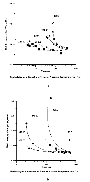
temperature in various times is shown for silver in Figure 1 a and for copper
in Figure 1 b
with the maximum temperature reached as a parameter. It can be seen that a
dramatic
decrease in resistivity occurs in a few seconds at high temperatures. It is
this very rapid
conversion of poorly consolidated metal particulates to nearly solid metal at
temperatures
less than half the melting point of the bulk metal which characterizes the
present
invention. The reaction occurs at a lower temperature with silver than with
copper. The
asymptotic resistivity of silver is approximately twice that of bulk silver.
For copper it is
approximately three times bulk.
Chemistry of Metallo-Organic Decomposition in the Presence of Metal Powders
It is believed that an extraordinary reaction is taking place between the ROM
and
metal powder constituents of the compositions of this invention which promotes
consolidation.
The evidence for this is two fold:
1) The consolidation of the metal powder to a solid metal conductor is
extremely
rapid.
2) The consolidation of the metal powder to a solid metal conductor occurs at
a
much lower temperature than conventional sintering to produce solid metal
objects from
16
CA 02451636 2003-12-22
WO 03/003381 PCT/USO1/20575
metal powders, as practiced in the powder metal industry and in the thick-film
electronic
industry.
The results shown in Figures 1 a and 1 b could not possibly be produced by
conventional sintering or by conventional thick filin technology. Sintering is
a time-
temperature process in which necks form between particles in contact which
grow by bulk
solid diffusion until the original particle compact is transformed into a
solid metal body.
The activation energy for bulk diffusion is of the order of 45-60 Kcal/mole
(180-250
J/mole) for copper, silver and gold. Typically copper is sintered at
650°C to 900° C, and
sintering times range from minutes to hours at pressures of tons per square
inch.
( Handbook of Powder Metallurgy, Henry H. Hausner, Ed., Chemical Publislung
Co, Inc.
NY, NY, p 164-167, 1973), The rate of sintering at 325° C can be
expected to be lower
than that at the usual thick film sintering temperature of 850°C by a
factor of seventy
million (7 x 10⁷). A ten minute process at 850° C will take 1300 years
at 325° C.
It may be that the finely divided metal powders have a higher surface energy
than
bulk metal, and in the ROM environment in which they are processed, they are
free of
surface layers which would inhibit metal-to-metal contact and consolidation.
The surface energy of the noble metals is as follows;
Cu 1670 ergs, cm 1047C
Ag 1140 ergs, cm~ ~ 907C
Au 1410 ergs, cm~ ~ 1027
C
(Chemistry ifz Two DimetZSiohs-Surfaces, G.A. Somofjai, Co~hell University
Press, (1981)
Fox copper, the excess surface energy of a 10 nanometer particle over the bulk
solid is
only 6800 J/mole compared to the activation energy for bulk diffusion of
250,000 J/mole.
It does not seem that even colloidal metal could have enough surface energy to
consolidate by bulk diffusion.
Surface diffusion is known to occur at much lower temperatures than bulk
diffusion. A transition temperature exists above which surface diffusion is
rapid, and this
temperature is found empirically to be approximately 1/3 the melting point in
degrees K.
(Thin Filin Deposition; Principles and Practices, D.L. Smith, McGraw Hill,
1995 p 170).
For silver this transition temperature is 138° C, so surface diffusion
could play a part at
17
CA 02451636 2003-12-22
WO 03/003381 PCT/USO1/20575
the temperatures at which consolidation is observed to take place. It is
difficult, however,
to imagine how a surface process could weld together the relatively massive
particles
which constitute the bulk of the metal in the compositions of this invention.
Another explanation for these findings is that in the ROM-metal powder
mixtures,
the metallo-organic compound decomposes directly onto the preexisting metal
particles,
welding them together by:
AgCOOC9Hlg + Ag metal ~ More Ag metals + organicsT
rather than by precipitation of new metal particles which then aggregate.
There is likely to
be an optimum metal surface to volume ratio large enough to provide adequate
area to
nucleate metallo-organic decomposition but small enough to permit binding the
metal
particles together into a solid deposit with the metallo-organic compound
available. The
preexisting metal unquestionably provides a rigid framework, preventing
shrinkage of the
deposited metal and spreading of the molten ROM during decomposition which
otherwise
results in poor definition, poor adhesion and breaks in the traces.
It may be that the colloidal particles added to the compositions of this
invention
are themselves a source of additional metallo-organic by
Ag colloid + HCOOCgHI9 ~ AgCOOC9H19
providing a mechanism whereby the ROM can transport metal from high surface
energy
particles and edges to low surface axea crevices and surfaces to consolidate
the metal
particles by a "chemical welding" process.
The ability to print high quality solid metal circuit traces on printed
circuit boards
has been sought for many years by many people skilled in the related arts.
This
experience is summarized above. The Ormet Transient Liquid Phase technology is
one
approach. The most widespread is the so-called polymer thick filin technology
based on
silver-loaded and carbon-loaded epoxies. None of these methods produce traces
which are
the equal of those based on conventional high temperature thick film materials
in a
simple, rapid print-and-heat cycle provided by the methods of this invention.
18
CA 02451636 2003-12-22
WO 03/003381 PCT/USO1/20575
Both gold and silver mixtures can be heated in air since the elemental metals
are
the stable form at the temperature at which the metallo-organic constituent
decomposes.
Copper, however, requires the use of a protective atmosphere to prevent the
formation of
copper oxide which is the stable product of decomposition in air. A nitrogen
atmosphere
containing less than about 50 and most preferably less than 10 ppm by volume
of oxygen
has been found to be suitable as shown in Figure 2. Addition of water vapor in
the amount
of about 3% has proven to be helpful in improving the conductivity of the
resulting
deposits as shown in Figure 3.
Printing Processes using the Compositions of this Invention
Polymer Thick Film and Polymer Metallizing
Polymer thick film technology uses mixtures of carbon or metal powders or
flakes
in polymer adhesives, primarily epoxies, to make printable mixtures. These can
be
applied to polymer substrates and cured at temperatures up to 176°C to
create conductor
patterns in the same way that thick film inks and pastes are applied to
ceramic and glass
substrates at higher temperatures.
Polymer metallizing is used to provide a conductive layer on polymer parts
such
as desk top computer housings, usually for electrical shielding. Again, carbon
or metal
particles are suspended in a paint or other organic coating material.
Typically, the carbon coatings are substantially less electrically conducting
than
the metal-based coatings. The best are silver flake-loaded epoxies which can
have
resistivities as low as 50-60 microohm-cm.
There are applications in which the electrical conductivity achievable with
metal-
loaded epoxies is not adequate. Furthermore, the conductivity of conventional
polymer
thick film materials is not stable over time due to changes in the resistance
of the
adventitious contacts between the individual silver flakes which give them
their
conductivity. Mechancal stresses, thermal expansion and corrosion can all play
a role in
this degradation.
The present invention provides an alternative to conventional polymer thick
film
compositions which can be cured at a temperature which a polymer-based
substrate can
19
CA 02451636 2003-12-22
WO 03/003381 PCT/USO1/20575
withstand, while providing an electrical conductivity comparable to the pure
metal and at
least a factor of ten greater than the best polymer thick films.
The compositions of this invention may be applied to the adhesive-coated
polymer
substrates by any convenient printing process.
An advantage of printable metallization compounds is that three dimensional
objects can be metallized which is not possible with metal foil and very
difficult with
sputtered or evaporated metal.
Flexible Circuit Patches
In many cases it is desired to add a few circuit traces to an existing printed
circuit,
either to repair mistakes, to implement changes or to complete the design
without the
expense of producing a complete multilayer circuit. This is difficult to do by
conventional
means, particularly when the traces must cross other traces, as they usually
do. This
invention provides a simple and inexpensive method for printing additional
traces over
the polymer coverlay or solder mask which is used as a final coat on most
flexible and
rigid printed circuits. Additional circuit traces connecting exposed metal
contact pads are
printed on the polymer surface and cured to solid metal by heating to a
temperature which
the polymer components can withstand. The method can also be used to create
new metal
pads and to bond components to the existing pads to complete the assembly of
the circuit.
A hybrid technology can be employed in which a photoresist is used to define
the
conductor traces with high resolution and the conductors themselves are
installed by
printing and heating the mixtures of this invention. The process is
illustrated
schematically in Figure 4 a.
The heat treating process is done under conditions very similar to soldering
and in
similar equipment. Additional cost savings can be realized by combining the
curing of
crossover traces and attachment of components. This is accomplished by
printing
additional material on the attachment pads for the components to be mounted on
the
circuit, placing the components on the uncured material with optional addition
of
additional material to the components themselves by printing or dipping, and
heat treating
the assembly to simultaneously consolidate and bond the additional traces and
bond the
components to the circuit, as shown in Figure 4b
CA 02451636 2003-12-22
WO 03/003381 PCT/USO1/20575
To achieve the ultimate in high resolution circuit traces, the presently
disclosed
technology can be combined with photo sensitive materials to create a hybrid
technology,
as shown in Figure 4 c. A photosensitive resist or solder mask is applied to
the surface of
the circuit and exposed to the desired pattern of conductor traces, which can
be very fine.
The negative image is developed in the usual way be washing the unpolymerized,
unexposed material away. The mixture of the present disclosure is applied by
printing or
doctor blading it into the circuit traces. Components may be placed at this
stage if desired
to make the circuit traces and assemble the circuit simultaneously, as
described above.
The circuit is heat treated in an oven which consolidates the mixture and
completely
polynerizes the resist or solder mask into an infusible, insoluble dielectric.
An additional
layer of solder mask or potting compound can be applied to protect the
finished circuit in
the usual way.
Printed Circuit Inner Layers
Most contemporary printed circuits are multilayers with attachment pads for
components on the two surfaces and the bulk of the circuit connections on thin
inner
layers. The inner layers are laminated between the two surface layers to make
the
completed multilayer circuit. Inner layers are produced by the same technology
as outer
layers and conventional single sided and double sided printed wiring boards.
The inner
layer substrate is similar to conventional glass reinforced epoxy FR-4
material but much
thinner. The minimum is about 0.004 inches thick, limited by the fact that it
is
conventional to use two layers of glass fabric to avoid single strands of
glass going from
side to side and acting as potential short circuit paths. The epoxy-glass is
laminated to
copper foil on one or both sides to provide the electrical conductors to be
developed by
etching and/or plating.
To produce a finished inner layer, the copper clad substrate is laminated to a
dry
film resist or coated with a liquid resist. It is then exposed to ultraviolet
light to partially
polymerize the resist, which is usually an acrylic-epoxy mixture. The
unexposed resist is
removed by a weak caustic or solvent wash to develop a negative image. The
image is
then converted to circuitry by etching away the exposed copper to leave
circuit traces
protected by resist which is stripped by strong caustic. An alternative method
is to
21
CA 02451636 2003-12-22
WO 03/003381 PCT/USO1/20575
electroplate copper followed by tin-lead etch resist on the exposed copper,
strip the
polymer resist and etch away the unprotected original copper foil.
The finished inner layers are stacked with the outer layers on the outside of
the
stack and with interleaving sheets of "prepreg" which is two layers of glass
cloth
impregnated with B-stage epoxy resin . The stack is then cured in a laminating
press
typically at 400 psi, 350°F for an hour. Often a vacuum press is used
to remove entrained
air and improve quality.
It can be seen that producing inner layers is a time-consuming and expensive
process. The resist costs approximately $1.00 per square foot, and the
lamination process
is exacting, as is the exposure. The cost of copper foil laminated to the
substrate is of the
order of $3 per square foot, and most of it is etched away. The development
step is time-
consuming and produces hazardous waste. The etching step suffers from the same
problems, as does the resist stripping process. There are numerous
intermediate rinses and
washes which have not been described separately which add to the cost. The
average layer
count, industry-wide in the U.S. is approximately seven. Many multilayer
circuits have 20
or more layers. It can be seen that production of inner layers is a major
expense. Total
production in the U.S. is approximately a billion square feet of inner layer
per year.
The compositions and processes of this invention replace this complexity with
a
simple print-and-heat technique which can produce inner layers very rapidly
and very
economically. The inner layer material is simply cleaned, printed and heat
treated in an
oven to convert the image to circuit conductors. The printed layers are then
laminated in
the usual way.
For still greater economies and higher production rates, the conductor pattern
can
be applied to a continuous web of substrate by a rotary press, much like
priilting a
newspaper but with finer resolution, as shown in Figure 5 a. Gravure printing
can be used
in this application. Offset printing can produce very high resolution also.
Ink jet printing
and electrostatic printing at high speeds are candidates. Following the
printing step, the
circuits will be cured in an oven, still as a continuous web. The ability of
these mixtures
to cure to solid metal in seconds is critical to realizing this concept.
Longer processing
times would make the oven disproportionately large relative to the press and
squander
much of the speed advantage of high speed printing.
22
CA 02451636 2003-12-22
WO 03/003381 PCT/USO1/20575
The individual layers can then be cut apart and laminated in the usual way.
Long
term, for very high production runs, the newspaper analogy can be pushed
further with
multiple rotary presses turning out inner layers simultaneously wluch are
cured in a single
oven and perhaps laminated on the fly before die cutting to size. The
lamination would be
done by interleaving the hot, cured inner layers with hot prepreg and pressing
them
between rolls to expel the air between layers and bond the stack. After
cooling, the stacks
would be cut apart to create individual the circuits. A still less expensive
approach is to
use the adhesive on the back surface of single sided inner layers to laminate
the stack
without the use of prepreg. The process is illustrated schematically in Figure
5 b
Direct Chip Attach and TAB Bonding
The leading edge of electronic packaging technology is now the direct
attachment
of Integrated Circuits (ICs) to Printed Wiring Boards (PWBs). The conventional
method
of packaging ICs is to cement them into a ceramic or plastic chip carrier and
wire bond
the individual input/output pads on the IC to individual pins on a metal lead
frame. The
IC is then potted in plastic or ceramic and covered with a lid for protection.
The leads are
separated from the frame and bent to shape for insertion into a socket or for
soldering
directly to pads on the PWB (surface mount tecluiology).
These packages and the wire bonding operation are expensive, and the packaged
semiconductors take up several times as much room as the ICs themselves. With
the
intense pressure for smaller devices and lower costs, there is a great
incentive to eliminate
the package and bond the IC direct to the PWB. An intermediate step is to
replace the
package and the wire bonding operation by bonding the IC to a lead frame which
can then
be bonded to the PWB. Since the lead frames in question axe produced by
etching metal
laminate on a continuous polyimide tape, this technology is referred to as
Tape
Automated Bonding (TAB).
Some Chip on Board (C~B) direct attaclunent is done by wire bonding the IC to
pads on the PWB, but this, while conventional and reliable, is expensive and
time
consuming. Both TAB bonding and the more advanced COB applications are gang
bonded by "bumping" the pads on the IC with added metal and soldering the
bumps to
mating pads on the tape or the PWB. The bumping process itself is time-
consuming and
23
CA 02451636 2003-12-22
WO 03/003381 PCT/USO1/20575
expensive because it is done by depositing a number of metallic layers under
vacuum
using photolithographic techniques. Preparing the tapes or circuit pads is
expensive
because it is at the limit of resolution of conventional subtractive etclung
technology with
50 micron (0.002 inch) lines and spaces. The tapes are further processed to
remove the
polymer in the center portion leaving very fine and fragile metal fingers
pointing in
toward the IC which can be individually bonded to the pads. A technology in
which ICs
could be gang bonded to traces on a PWB or a polyimide tape in a single
operation could
achieve a major simplification and cost reduction. The compositions of the
present
invention can be applied to ICs and/or to polymer-based substrates to act as a
bonding
agent to secure the IC to the substrate with all the electrical connections
made
simultaneously and reliably.
The pads on ICs were once almost universally made of aluminum, which is
compatible with the silicon semiconductor, is a good electrical conductor and
is easily and
economically applied by evaporation or sputtering. Aluminum is not easy to
bond to due
to the very tenacious native oxide which protects the aluminum surface from
oxidation
and corrosion. Wire bonding and chip bumping have to overcome this obstacle to
obtain
reliable bonds. In the case of wire bonding, the connections are made to balls
formed on
the end of 0.001 inch diameter gold wire by welding them to the aluminum,
usually by
ultrasonic agitation to mechanically disrupt the oxide film and cold weld the
gold to the
aluminum. In the case of chip bumping, a layer of an intermediate bonding
metal such as
titanium-tungsten alloy is deposited by sputtering to make contact with the
aluminum and
isolate it from the material of the bump which is deleterious to the silicon.
Other layers
are added as well as the copper or solder bump material. All of these
operations require
photolithographic masking and are quite expensive. A polyimide insulating
layer is often
applied to the surface of the chip to protect it from the subsequent
processing by covering
all but the pads .
More recently copper metallization has become increasingly used for the final
metallization on chips following its introduction by IBM in 1997, IBMResea~ch
Magazirae, Vol. 35, No. 4 (1997). The advantage of copper in this application
is better
electrical conductivity than aluminum but it also makes it possible to use the
mixtures of
this invention to bump and bond chips easily and at low cost.
24
CA 02451636 2003-12-22
WO 03/003381 PCT/USO1/20575
Two methods of applying the compositions of this invention to chips are as
follows:
Method 1
1) Print the composition on the copper pads to a thickness wluch will produce
the
desired biunp height after curing.
2) Cure the composition to produce solid metal bumps.
Method 2
1) Add a photo patterned polyimide or other dielectric insulating layer to
chip
surface as is now done.
2) Squeegee or print the composition to create the bumps.
3) Cure as before.
4) Chemical-mechanical polish the surface to planarize and remove excess
metal.
The compositions of this invention may be applied to the IC by any convenient
printing process. Tests have been done by screen printing conductor images.
The mixtures
have also been applied by stenciling and ink jet printing. Gravure printing,
both direct and
offset can be used to produce fine line images. Offset and lithographic
methods can be
used.
The bumped chips of this invention must be attached either to a polyimide tape
or
a PWB with matclung metallic circuit traces. Such traces may be produced by
the
methods of this invention by a simple print-and-heat process with high
resolution
Additional printing processes are applicable to polymer films which are not
applicable to
ICs. In particular electrostatic methods (xerography) is possible and along
with ink jet
printing provides the ability to generate conductor patterns direct from CAD'
files. This
provides great flexibility in design and in small quantity manufacture and
inventory
control.
The highest possible resolution is provided by photolithographic techniques
and a
hybrid technology in wluch the dielectric is patterned photographically and a
composition
of this invention is printed or doctor bladed into the grooves is a highly
reliable and
promising way to produce very fine conductor patterns for TAB and direct
attach
CA 02451636 2003-12-22
WO 03/003381 PCT/USO1/20575
The next highest resolution may be provided by electrostatic printing with
liquid
toner suspensions with particle diameters of a few microns.. S.P. Schmidt, et
al.,
"Handboole of Imaging Materials", Chapter 5, pp. 227-252, A.S. Daimond, Ed.,
(Marcel
Dekker, NY).
Following printing of the IC and the substrate, the bonding process may be
carried
out in several ways.
1) Both sets of contacts can be cured and additional composition printed on
and
reheated similar to soldering. (Solder could also be used as is now done, but
the
compositions of this invention provide a superior solution by virtue of not
needing a flux
removal step and not introducing extraneous metals into the sensitive
semiconductor
contact.)
2) One set of contacts can be heat treated and the other printed and adhered
to the
first before reheating to achieve the bond.
3) One set of contacts only is printed and the other component is adhered to
it
prior to heat treating to achieve the application and the bond simultaneously.
Following printing, the image is converted to metal by heating in an oven.
Examples
The examples described below indicate how the individual constituents of the
preferred compositions and the conditions for applying them function to
provide the
desired result. The examples will serve to further typify the nature of this
invention, but
should not be construed as a limitation in the scope thereof. which scope is
defined solely
in the appended claims.
Example 1
A mixture of 52 parts by weight of-325 mesh spherical copper powder (Cerac C-
1241, 30 parts by weight of 2-3 micrometer spherical copper powder (Cerac C-
1229) , 8
parts by weight colloidal copper powder with a mean diameter of approximately
0.1
micrometer made by reducing copper acetate in ethylene glycol with hydrazine
hydrate
(the well-known glycol synthesis), and 10 parts by weight neodecanoic acid
(Exxon
Chemical Prime Grade) was prepared. The mixture was combined and blended by
hand in
26
CA 02451636 2003-12-22
WO 03/003381 PCT/USO1/20575
a nitrogen glove box. The mixture was roll milled in air to produce a
homogeneous ink.
The ink was screen printed onto a DuPont Kapton~ ELJ dielectric substrate at
room
temperature in air. The traces were heat treated in a belt furnace at
330°C for 6-10 minutes
in the hot zone in a NZ H20-Hz atmosphere.
After heating, the components were dry to the touch, the organic constituents
having been completely removed. The electrical resistivity of the bright
copper circuit
trace measured by IPC Test Method 2.5.13 was 0.41 g-ohms per m2 compared to
bull
copper at 0.15 gram-ohms per m2. Scotch tape was applied to the circuit trace
and
immediately removed at a 90° angle to determine the bond strength of
the copper to the
substrate. No metal was removed with the tape.
Example 2
A mixture 72 parts by weight of 2-3 micrometer diameter spherical copper
powder
(Cerac C-1229, 16 parts by weight colloidal copper powder with a mean diameter
of
approximately 0.1 micrometer made by reducing copper acetate in ethylene
glycol with
hydrazine hydrate, and 12 parts by weight neodecanoic acid (Exxon Chemical
Prime
Grade) was prepared. The mixture was combined and blended by hand in a glove
box.
The mixture was roll milled in air to produce homogeneous ink. The inl~ was
screen
printed onto a DuPont Kapton~ ELJ dielectric substrate at room temperature in
air. The
traces were heat treated in a belt furnace at 330°C for 6-10 minutes in
the hot zone in a
NZ H20-HZ atmosphere.
After heating, the components were dry to the touch, the organic constituents
having been completely removed. The electrical resistivity of the bright
copper circuit
trace measured by IPC Test Method 2.5.13 was 0.47 g-ohms per m2. Scotch tape
was
applied to the circuit trace and immediately removed at a 90° angle to
determine the bond
strength of the copper to the substrate. No metal was removed with the tape.
Example 3
A mixture 57 parts by weight of 0.5 micrometer diameter spherical copper
powder
(Canadian Electronic Powders Corp St. Laurent Quebec, Canada, Cu-0500), 23
parts by
27
CA 02451636 2003-12-22
WO 03/003381 PCT/USO1/20575
weight colloidal copper powder with a mean diameter of approximately 0.1
micrometers
made by reducing copper acetate in ethylene glycol with hydrazine hydrate, and
20 parts
by weight of neodecanoic acid (Exxon Chemical Prime Grade) was prepared. . The
mixture was combined and blended by hand in a glove box. The mixture was roll
milled
in air to produce a homogeneous ink. The ink was screen printed onto a DuPont
I~apton0
ELJ dielectric substrate at room temperature in air. The traces were heat
treated in a belt
furnace at 330°C for 6-10 minutes in the hot zone in a NZ-H20-Hz
atmosphere.
After heating, the components were dry to the touch, the organic constituents
having been completely removed. The electrical resistivity of the bright
copper circuit
trace measured by IPC Test Method 2.5.13 was 0.47 g-ohms per m2. Scotch tape
was
applied to the circuit trace and immediately removed at a 90° angle to
determine the bond
strength of the copper to the substrate. No metal was removed with the tape.
Example 4
A mixture of 11 parts by weight of-325 mesh spherical copper powder (Cerac C-
1241), 31 parts by weight of 2-3 micrometer spherical copper powder (Cerac C-
1229), 12
parts by weight of 0.5 ~,m spherical Cu powder (Canadian Electronic Powders
Corp, St.
Laurent Quebec, Canada, Cu-0500), 26 parts by weight colloidal copper powder
with a
mean diameter of approximately 0.1 micrometer made by reducing copper acetate
in
ethylene glycol with hydrazine hydrate , and 20 parts by weight neodecanoic
acid (Exxon
Chemical Prime Grade) was prepared.
The mixture was combined and blended by hand in a nitrogen glove box. The
mixture was roll milled in air to produce a homogeneous ink. The ink was
screen printed
onto a I~apton~ ELJ dielectric substrate at room temperature in air. The
traces were heat
treated in a belt furnace at 330°C for 6-10 minutes in the hot zone in
a NZ Hz0-HZ
atmosphere.
After heating, the components were dry to the touch, the organic constituents
having been completely removed. The electrical resistivity of the bright Cu
circuit trace
28
CA 02451636 2003-12-22
WO 03/003381 PCT/USO1/20575
(IPC TM 2.5.13) was measured to be 0.45 g-ohms per m2. Scotch tape was applied
to the
circuit trace and immediately removed at a 90° angle to determine the
bond strength of the
copper to the substrate. No metal was removed with the tape.
Example 5
A mixture comprising 25.0 g spherical silver powder (Technic, Inc., 0.6 micron
average diameter), 3.1 g silver neodecanoate, synthesized from ammonium
neodecanoate
and silver nitrate, and 5.4 g neodecanoic acid (Exxon Chemical Prime Grade)
was milled
on a 2-roll mill for 30 minutes.
The resulting silver ink was used to screen print a 600 square serpentine test
pattern onto a DuPont Kapton~ H polyimide substrate. The sample was run
through a
reflow furnace with an air atmosphere and heated to 240°C over a period
of 1 ~ minutes.
The resulting 23.7 cm long silver trace had a resistance of 2.35 S2. The cross-
sectional
area of the trace was determined to be 1x10 cmz using a Dektak IIA
profilometer. The
resistivity was calculated to be 9.9 ~.5~,-cm or 3.9 mS~lsq/mil compared to
1.59 ~.5~-cm for
bulk silver.
29