Language selection

Search

Patent 2452227 Summary

Third-party information liability

Some of the information on this Web page has been provided by external sources. The Government of Canada is not responsible for the accuracy, reliability or currency of the information supplied by external sources. Users wishing to rely upon this information should consult directly with the source of the information. Content provided by external sources is not subject to official languages, privacy and accessibility requirements.

Claims and Abstract availability

Any discrepancies in the text and image of the Claims and Abstract are due to differing posting times. Text of the Claims and Abstract are posted:

  • At the time the application is open to public inspection;
  • At the time of issue of the patent (grant).
(12) Patent Application: (11) CA 2452227
(54) English Title: PATCH DIPOLE ARRAY ANTENNA INCLUDING A FEED LINE ORGANIZER BODY AND RELATED METHODS
(54) French Title: ANTENNE RESEAU DIPOLE A PLAQUE COMPRENANT UN CORPS D'ORGANISATION DES LIGNES D'ALIMENTATION ET PROCEDES CORRESPONDANTS
Status: Deemed Abandoned and Beyond the Period of Reinstatement - Pending Response to Notice of Disregarded Communication
Bibliographic Data
(51) International Patent Classification (IPC):
  • H1Q 1/38 (2006.01)
  • H1Q 9/16 (2006.01)
  • H1Q 21/00 (2006.01)
  • H1Q 21/06 (2006.01)
  • H1Q 21/24 (2006.01)
(72) Inventors :
  • RAWNICK, JAMES J. (United States of America)
  • BOOZER, RANDY E. (United States of America)
  • TAYLOR, ROBERT C. (United States of America)
  • CLARK, WILLIAM E. (United States of America)
  • PERKINS, GILBERT R. (United States of America)
  • HECKAMAN, DOUGLAS E. (United States of America)
(73) Owners :
  • HARRIS CORPORATION
(71) Applicants :
  • HARRIS CORPORATION (United States of America)
(74) Agent: EDWARD H. OLDHAMOLDHAM, EDWARD H.
(74) Associate agent:
(45) Issued:
(86) PCT Filing Date: 2002-06-20
(87) Open to Public Inspection: 2003-01-09
Examination requested: 2003-12-29
Availability of licence: N/A
Dedicated to the Public: N/A
(25) Language of filing: English

Patent Cooperation Treaty (PCT): Yes
(86) PCT Filing Number: PCT/US2002/019542
(87) International Publication Number: US2002019542
(85) National Entry: 2003-12-29

(30) Application Priority Data:
Application No. Country/Territory Date
09/892,709 (United States of America) 2001-06-28

Abstracts

English Abstract


An antenna (10) includes a substrate (12) including a ground plane (26) and a
dielectric layer (24) adjacent thereto and at least one antenna unit (13)
carried by the substrate (12). The at least one antenna unit (13) may include
a plurality of adjacent antenna elements (14, 16, 18 and 20) arranged in
spaced apart relation from one another about a central feed position (22) on
the dielectric layer (24) opposite the ground plane (26). The at least one
antenna unit (13) may also include an antenna feed structure (30) including a
respective coaxial feed line (32) for each antenna element (14, 16, 18 and 20)
and a feed line organizer body (60) having passageways (61) therein for
receiving respective coaxial feed lines (32).


French Abstract

Une antenne (10) comprend un substrat (12) comportant un plan de sol (26) et une couche diélectrique (24) adjacente à ce dernier et au moins une unité d'antenne (13) supportée par le substrat (12). L'unité d'antenne (13) peut comprendre une pluralité d'éléments (14, 16, 18 et 20) d'antenne adjacents, qui sont disposés de manière espacée les uns par rapport aux autres autour d'une position centrale (22) d'alimentation sur la couche diélectrique (24) à l'opposé du plan de sol (26). L'unité d'antenne (13) peut également comprendre une structure d'alimentation (30) pour l'antenne comportant une ligne (32) d'alimentation coaxiale respective pour chaque élément (14, 16, 18 et 20) d'antenne et un corps (60) d'organisation des lignes d'alimentation dans lequel sont prévus des passages (61) permettant de recevoir les lignes (32) d'alimentation coaxiales respectives.

Claims

Note: Claims are shown in the official language in which they were submitted.


THAT WHICH IS CLAIMED IS:
1. An antenna comprising:
a substrate comprising a ground plane and a
dielectric layer adjacent thereto; and
at least one antenna unit carried by said substrate
comprising:
a plurality of adjacent antenna elements
arranged in spaced apart relation from one another
about a central feed position on said dielectric
layer opposite said ground plane, and
an antenna feed structure comprising a
respective coaxial feed line for each antenna
element and a feed line organizer body having
passageways therein for receiving respective coaxial
feed lines.
2. The antenna according to Claim 1 wherein said
feed line organizer body comprises:
a base connected to said ground plane; and
a guide portion carried by said base, said base and
guide portion being integrally formed as a monolithic unit.
3. The antenna according to Claim 2 wherein said
guide portion comprises:
a bottom enclosed guide portion carried by said
base;
a top enclosed guide portion adjacent said antenna
elements; and
an intermediate open guide portion extending between
said bottom enclosed guide portion and said top enclosed guide
portion.
4. The antenna according to Claim 3 wherein each
coaxial feed line is soldered to said feed line organizer body
at said intermediate open guide portion.
9

5. The antenna according to Claim 2 wherein said
antenna feed structure further comprises a tuning plate carried
by said guide portion.
6. The antenna according to Claim 1 wherein said
passageways are all parallel to a common axis.
7. The antenna according to Claim 1 wherein said
feed line organizer body comprises at least one conductive
material.
8. The antenna according to Claim 1 wherein said
ground plane extends laterally outwardly beyond a periphery of
said at least one antenna unit.
9. The antenna according to Claim 1 further
comprising at least one hybrid circuit carried by said
substrate and connected to said antenna feed structure.
10. The antenna according to Claim 1 wherein each
antenna element has a generally rectangular shape.
11. The antenna according to Claim 1 wherein said
at least one antenna unit comprises a plurality of antenna
units arranged in an array.
12. The antenna according to Claim 1 wherein said
dielectric layer has a thickness in a range of about ~ an
operating wavelength of the at least one antenna unit.
13. The antenna according to Claim 1 further
comprising at least one impedance matching dielectric layer on
said at least one antenna unit.
-10-

14. An antenna comprising:
a substrate comprising a ground plane and a
dielectric layer adjacent thereto; and
at least one antenna unit carried by said substrate
comprising:
a plurality of adjacent antenna elements
arranged in spaced apart relation from one another
about a central feed position on said dielectric
layer opposite said ground plane, and
an antenna feed structure comprising a
respective coaxial feed line for each antenna
element and a feed line organizer body having
passageways therein for receiving respective coaxial
feed lines, said passageways all being parallel to a
common axis and said feed line organizer body being
integrally formed as a monolithic unit.
15. The antenna according to Claim 14 wherein said
feed line organizer body comprises:
a base connected to said ground plane; and
a guide portion carried by said base.
16. The antenna according to Claim 15 wherein said
guide portion comprises:
a bottom enclosed guide portion carried by said
base;
a top enclosed guide portion adjacent said antenna
elements; and
an intermediate open guide portion extending between
said bottom enclosed guide portion and said top enclosed guide
portion.
17. The antenna according to Claim 16 wherein each
coaxial feed line is soldered to said feed line organizer body
at said intermediate open guide portion.
-11-

18. The antenna according to Claim 15 wherein said
antenna feed structure further comprises a tuning plate carried
by said guide portion.
19. The antenna according to Claim 14 wherein said
feed line organizer comprises at least one conductive material.
20. The antenna according to Claim 14 wherein said
ground plane extends laterally outwardly beyond a periphery of
said at least one antenna unit.
21. The antenna according to Claim 14 further
comprising at least one hybrid circuit carried by said
substrate and connected to said antenna feed structure.
22. The antenna according to Claim 14 wherein each
antenna element has a generally rectangular shape.
23. The antenna according to Claim 14 wherein said
at least one antenna unit comprises a plurality of antenna
units arranged in an array.
24. The antenna according to Claim 14 wherein said
dielectric layer has a thickness in a range of about 1/2 an
operating wavelength of the at least one antenna unit.
25. The antenna according to Claim 14 further
comprising at least one impedance matching dielectric layer on
said at least one antenna unit.
26. A method for making an antenna comprising:
providing at least one antenna unit on a substrate
comprising a ground plane and a dielectric layer adjacent
thereto, the at least one antenna unit comprising a plurality
of adjacent antenna elements arranged in spaced apart relation
from one another about a central feed position on the
-12-

dielectric layer opposite the ground plane, the substrate
having an opening therein exposing portions of the plurality of
adjacent antenna elements;
forming an antenna feed structure by positioning
respective coaxial feed lines within passageways of a feed line
organizer body; and
inserting the antenna feed structure into the
opening and connecting each of the coaxial feed lines to a
respective antenna element.
27. The method according to Claim 26 wherein the
feed line organizer body comprises a base and a guide portion
carried by the base, the base and guide portion being
integrally formed as a monolithic unit; and wherein inserting
the antenna feed structure into the opening comprises
connecting the base to the ground plane and connecting each
coaxial cable to a respective antenna element.
28. The method according to Claim 27 wherein the
guide portion comprises:
a bottom enclosed guide portion carried by the base;
a top enclosed guide portion to be positioned
adjacent the antenna elements; and
an intermediate open guide portion extending between
the bottom enclosed guide portion and the top enclosed guide
portion.
29. The method according to Claim 28 wherein
forming the antenna feed structure further comprises soldering
each coaxial feed line to the feed line organizer body at the
intermediate open guide portion.
30. The method according to Claim 27 wherein
forming the antenna feed structure further comprises connecting
a tuning plate to the guide portion.
-13-

31. The method according to Claim 26 wherein the
passageways are each parallel to a common axis.
32. The method according to Claim 26 wherein the
feed line organizer comprises at least one conductive material.
33. The method according to Claim 26 wherein the
ground plane extends laterally outwardly beyond a periphery of
the at least one antenna unit.
34. The method according to Claim 26 further
comprising providing at least one hybrid circuit on the
substrate and connected to the antenna feed structure.
35. The method according to Claim 26 wherein each
antenna element has a generally rectangular shape.
36. The method according to Claim 26 wherein
providing the at least one antenna unit comprises arranging a
plurality of antenna units in an array.
37. The method according to Claim 26 wherein the
dielectric layer has a thickness in a range of about 1/2 an
operating wavelength of the at least one antenna unit.
38. The method according to Claim 26 further
comprising providing at least one impedance matching dielectric
layer on the at least one antenna unit.
-14-

Description

Note: Descriptions are shown in the official language in which they were submitted.


CA 02452227 2003-12-29
WO 03/003510 PCT/US02/19542
PATCH DIPOLE ARRAY ANTENNA INCLUDING A FEED NINE
ORGANIZATION BODY AND RELATED METHODS
Related Application
The present application is a continuation-in-part of U.S.
Application No. 09/702,712, filed October 31, 2000.
Field of the Invention
The present invention relates to the field of
communications, and more particularly, to phased array
antennas.
Background of the Invention
Existing microwave antennas include a wide variety of
configurations for various applications, such as satellite
reception, remote broadcasting, or military communication. The
desirable characteristics of low cost, light-weight, low
profile and mass producibility are provided in general by
printed circuit antennas wherein flat conductive elements are
spaced from a single essentially continuous ground element by a
dielectric sheet of uniform thickness. The antennas are
designed in an array and may be used for communication systems
such as identification of friend/foe (IFF) systems, personal
communication service (PCS) systems, satellite communication
systems, and aerospace systems, which require such
characteristics as low cost, light weight, low profile, and a
low sidelobe.
The bandwidth and directivity capabilities of such
antennas, however, can be limiting for certain applications
such as space applications. Furthermore, while a microstrip
patch antenna is advantageous in applications requiring a
conformal configuration, e.g. in aerospace systems, mounting
the antenna presents challenges with respect to the manner in
which it is fed such that conformality and satisfactory
radiation coverage and directivity are maintained and losses to
surrounding surfaces are reduced.
-1-

CA 02452227 2003-12-29
WO 03/003510 PCT/US02/19542
More specifically, increasing the bandwith of a phased
array antenna with a wide scan angle is conventionally achieved
by dividing the frequency range into multiple bands. This
approach results in a considerable increase in the size and
weight of the antenna while creating a Radio Frequency (RF)
interface problem. Also, gimbals have been used to
mechanically obtain the required scan angle. Again, this
approach increases the size and weight of the antenna, and
results in a slower response time.
Additionally, prior art phased array antennas often have
an antenna feed structure including coaxial feed lines to be
connected to the various antenna elements. These coaxial feed
lines are typically parallel to a common axis and soldered
together to form the antenna feed structure. The feed
structure is inserted through the antenna's substrate for
connection with the antenna elements. Yet, it may be difficult
to properly ground such antenna feed structures while
connecting them to the antenna elements, which may result in
undesirable common mode currents, for example.
Thus, there is a need for a lightweight patch dipole
phased array antenna with a wide frequency bandwith and a wide
scan angle, and that can be conformally mountable to a surface.
Summary of the Invention
In view of the foregoing background, it is therefore an
object of the invention to provide a lightweight patch dipole
phased array antenna with a wide frequency bandwith and a wide
scan angle, and that can be conformally mountable to a surface.
This and other objects, features and advantages in
accordance with the present invention are provided by an
antenna including a substrate including a ground plane and a
dielectric layer adjacent thereto and at least one antenna unit
carried by the substrate. The at least one antenna unit may
include a plurality of adjacent antenna elements arranged in
spaced apart relation from one another about a central feed
position on the dielectric layer opposite the ground plane.

CA 02452227 2003-12-29
WO 03/003510 PCT/US02/19542
The at least one antenna unit may also include an antenna feed
structure including a respective coaxial feed line for each
antenna element and a feed line organizer body having
passageways therein for receiving respective coaxial feed
lines.
More specifically, the feed line organizer body may
include a base connected to the ground plane and a guide
portion carried by the base. The base and the guide portion
may be integrally formed as a monolithic unit, for example.
Moreover, the guide portion may include a bottom enclosed guide
portion carried by the base, a top enclosed guide portion
adjacent the antenna elements, and an intermediate open guide
portion extending between the bottom enclosed guide portion and
the top enclosed guide portion adjacent the antenna elements.
Each coaxial feed line may be soldered to the feed line
organizer body at the intermediate open guide portion.
Furthermore, the antenna feed structure may include a tuning
plate carried by the guide portion. Additionally, the
passageways may each be parallel to a common axis, and the feed
line organizer may include at least one conductive material,
such as brass, for example.
The ground plane may extend laterally outwardly beyond a
periphery of the at least one antenna unit. Also, the antenna
may further include at least one hybrid circuit carried by the
substrate and connected to the antenna feed structure. Each
antenna element may have a generally rectangular shape, and the
at least one antenna unit may include a plurality of antenna
units arranged in an array. Furthermore, the dielectric layer
may have a thickness in a range of about '-~ an operating
wavelength of the at least one antenna unit. Additionally,
there may be at least one impedance matching dielectric layer
on the at least one antenna unit.
A method aspect of the invention is for making an antenna
and includes providing at least one antenna unit on a substrate
comprising a ground plane and a dielectric layer adjacent
thereto. The at least one antenna unit may include a plurality
-3-

CA 02452227 2003-12-29
WO 03/003510 PCT/US02/19542
of adjacent antenna elements arranged in spaced apart relation
from one another about a central feed position on the
dielectric layer opposite the ground plane. Additionally, the
substrate may have an opening therein exposing portions of the
plurality of adjacent antenna elements. The method may further
include forming an antenna feed structure by positioning
respective coaxial feed lines within passageways of a feed line
organizer body. Further, the antenna feed structure is
inserted into the opening, and each of the coaxial feed lines
is connected to a respective antenna element.
Brief Description of the Drawings
FIG. l is a schematic plan view of a dual polarization
phased array antenna in accordance with the present invention.
FIG. 2 is a cross-sectional view of the antenna including
the antenna feed structure taken along the line 2-2 in FIG. 1.
FIG. 3 is a perspective view of the feed line organizer
body of the antenna feed structure of FIG. 2.
FIG. 4 is a cross-sectional view of the ground plane,
dielectric layer, antenna units and impedance matching
dielectric layer of the antenna taken along the line 4-4 in
FIG. 1.
Detailed Description of the Preferred Embodiments
The present invention will now be described more fully
hereinafter with reference to the accompanying drawings, in
which preferred embodiments of the invention are shown. This
invention may, however, be embodied in many different forms and
should not be construed as limited to the embodiments set forth
herein. Rather, these embodiments are provided so that this
disclosure will be thorough and complete, and will fully convey
the scope of the invention to those skilled in the art. Like
numbers refer to like elements throughout.
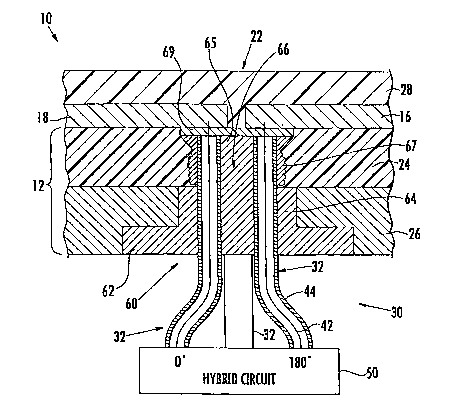
Referring to FIGS. 1-4, a dual polarization antenna 10
according to the invention will now be described. The antenna
10 includes a substrate 12 having a ground plane 26 and a
-4-

CA 02452227 2003-12-29
WO 03/003510 PCT/US02/19542
dielectric layer 24 adjacent thereto, and at least one antenna
unit 13 carried by the substrate. Preferably, a plurality of
antenna units 13 are arranged in an array. As shown in FIG. 1,
the antenna 10 includes nine antenna units 13. Each antenna
unit 13 includes four adjacent antenna patches or elements 14,
16, 18, 20 arranged in spaced apart relation from one another
about a central feed position 22 on the dielectric layer 24
opposite the ground plane 26. Preferably, diagonal pairs of
antenna elements, e.g. 16/18 and 14/20, define respective
antenna dipoles thereby providing dual polarization, as would
be appreciated by the skilled artisan. Of course, only a
single pair of antenna elements, e.g. 16/18, forming an antenna
dipole may be provided for a single polarization embodiment.
Each antenna unit also includes an antenna feed structure
30 including four coaxial feed lines 32. Each coaxial feed
line 32 has an inner conductor 42 and a tubular outer conductor
44 in surrounding relation thereto, for example (FIG. 2). The
antenna feed structure 30 includes a feed line organizer body
60 having passageways 61 therein for receiving respective
coaxial feed lines 32. The feed line organizer 60 is
preferably integrally formed as a monolithic unit, as will be
appreciated by those of skill in the art.
More specifically, the feed line organizer body 60 may
include a base 62 connected to the ground plane 26 and a guide
portion 63 carried by the base. The base 62 may have holes 68
therein so that the base may be connected to the ground plane
26 using screws. Of course, other suitable connectors known to
those of skill in the art may also be used.
The guide portion 63 may include a bottom enclosed guide
portion 64 carried by the base 62, a top enclosed guide portion
65 adjacent the antenna elements 14, 16, 18, 20, and an
intermediate open guide portion 66 extending between the bottom
enclosed guide portion and the top enclosed guide portion. The
outer conductor 44 of each coaxial feed line 32 may be
-5-

CA 02452227 2003-12-29
WO 03/003510 PCT/US02/19542
connected to the feed line organizer body 60 at the
intermediate open guide portion 66 via solder 67, as
illustratively shown in FIG. 2.
The feed line organizer body 60 is preferably made from a
conductive material, such as brass, for example, which allows
for relatively easy production and machining thereof. As a
result, the antenna feed structure 30 may be produced in large
quantities to provide consistent and reliable ground plane 26
connection. Of course, other suitable materials may also be
used for the feed line organizer body 60, as will be
appreciated by those of skill in the art.
Additionally, as illustratively shown in FIG. 3, the
passageways 61 are preferably parallel to a common axis A-A so
that the coaxial feed lines 32 are parallel and adjacent to one
another. Furthermore, the antenna feed structure 30 may
advantageously include a tuning plate 69 carried by the top
enclosed guide portion 65. The tuning plate 69 may be used to
compensate for feed inductance, as will be appreciated by those
of skill in the art.
The ground plane 26 may extend laterally outwardly beyond
a periphery of the antenna units 13, and the coaxial feed lines
32 may diverge outwardly from contact with one another upstream
from the central feed position 22, as can be seen in FIG. 2.
The antenna 10 may also include at least one hybrid circuit 50
carried by the substrate 12 and connected to the antenna feed
structure 30. The hybrid circuit 50 controls, receives and
generates the signals to respective antenna elements 14, 16,
18, 20 of the antenna units 13, as would be appreciated by
those skilled in the art.
The dielectric layer preferably has a thickness in a
range of about '~ an operating wavelength of the antenna 10, and
at least one impedance matching dielectric layer 28 may be
provided over the antenna units 13. This impedance matching
dielectric layer 28 may also extend laterally outwardly beyond
-6-

CA 02452227 2003-12-29
WO 03/003510 PCT/US02/19542
a periphery of the antenna units 13, as shown in FIG. 4. The
use of the extended substrate 12 and extended impedance
matching dielectric layer 28 result in an antenna bandwidth of
2:1 or greater. The substrate 12 is flexible and can be
conformally mounted to a rigid surface, such as the nose-cone
of an aircraft or spacecraft, for example.
A related method aspect of the invention is for making
the antenna 10. The method includes providing at least one
antenna unit 13 on the substrate 12, which includes the ground
plane 26 and the dielectric layer 24 adjacent thereto. The at
least one antenna unit 13 includes a plurality of adjacent
antenna elements 14, 16, 18, 20 arranged in spaced apart
relation from one another about the central feed position 22 on
the dielectric layer 24 opposite the ground plane 26. As noted
above, the substrate 12 includes an opening exposing portions
of the antenna elements 14, 16, 18, 20.
The method further includes forming the antenna feed
structure 30 by positioning respective coaxial feed lines 32
within the passageways 61 of the feed line organizer body 60,
as described above. Furthermore, the method also includes
inserting the antenna feed structure 30 into the opening and.
connecting the coaxial feed lines 32 to respective antenna
elements 14, 16, 18, 20, as previously discussed above.
More specifically, the feed line organizer body 60 allows
the antenna feed structure 30 to essentially be "plugged in" to
the substrate 12 for relatively easy connection to the at least
one antenna unit 13. The antenna feed structure 30 including
the feed line organizer body 60 also allows for relatively easy
removal and/or replacement without damage to the antenna 10.
Moreover, common mode currents, which may result from improper
grounding of the coaxial feed lines 32 may be substantially
reduced using the antenna feed structure 30 including the feed
line organizer body 60. That is, the intermediate open guide
_7_

CA 02452227 2003-12-29
WO 03/003510 PCT/US02/19542
portion 66 thereof allows for consistent and reliable grounding
of the coaxial feed lines 32.
The antenna 10 may have a two-to-one bandwidth in the
frequency range of 2-28 GHz, may achieve a scan angle of +45°,
and provide return loss of less than or equal to about l0db.
Thus, a lightweight patch dipole phased array antenna 10
according to the invention with a wide frequency bandwith and a
wide scan angle is provided. Also, the antenna 10 is flexible
and can be conformally mountable to a surface.
Furthermore, while the antenna feed structure 30 has been
described for use with the four antenna elements 14, 16, 18,
20, it will be appreciated by those of skill in the art that
this feed structure is also well suited for antenna arrays with
different numbers of antenna elements. Moreover, the antenna
feed structure 30 may also be used with antennas other than the
antennas 10 discussed herein. By way of example, the antenna
feed structure 30 according to the invention is also well
suited for use with antennas such as the phased array antenna
disclosed in U.S. Application No. 09/703,247 filed October 31,
2000, and assigned to the present assignee, which is hereby
incorporated herein in its entirety by reference. Application
to numerous other antenna structures may also be possible, as
will be appreciated by those of skill in the art.
Many modifications and other embodiments of the invention
will come to the mind of one skilled in the art having the
benefit of the teachings presented in the foregoing
descriptions and the associated drawings. Therefore, it is
understood that the invention is not to be limited to the
specific embodiments disclosed, and that modifications and
embodiments are intended to be included within the scope of the
appended claims.
_g-

Representative Drawing
A single figure which represents the drawing illustrating the invention.
Administrative Status

2024-08-01:As part of the Next Generation Patents (NGP) transition, the Canadian Patents Database (CPD) now contains a more detailed Event History, which replicates the Event Log of our new back-office solution.

Please note that "Inactive:" events refers to events no longer in use in our new back-office solution.

For a clearer understanding of the status of the application/patent presented on this page, the site Disclaimer , as well as the definitions for Patent , Event History , Maintenance Fee  and Payment History  should be consulted.

Event History

Description Date
Application Not Reinstated by Deadline 2009-06-22
Time Limit for Reversal Expired 2009-06-22
Deemed Abandoned - Conditions for Grant Determined Not Compliant 2008-08-28
Deemed Abandoned - Failure to Respond to Maintenance Fee Notice 2008-06-20
Notice of Allowance is Issued 2008-02-28
Letter Sent 2008-02-28
4 2008-02-28
Notice of Allowance is Issued 2008-02-28
Inactive: Received pages at allowance 2008-01-15
Inactive: Office letter 2008-01-04
Inactive: IPC removed 2007-09-06
Inactive: Approved for allowance (AFA) 2007-07-31
Amendment Received - Voluntary Amendment 2007-03-20
Inactive: S.30(2) Rules - Examiner requisition 2007-01-19
Inactive: IPC from MCD 2006-03-12
Letter Sent 2006-02-17
Inactive: Office letter 2006-02-17
Inactive: Correspondence - Transfer 2005-12-29
Inactive: Transfer information requested 2005-12-07
Inactive: Delete abandonment 2005-10-05
Inactive: Abandoned - No reply to Office letter 2005-08-18
Inactive: Correspondence - Transfer 2005-07-08
Inactive: Transfer information requested 2005-05-18
Inactive: Correspondence - Formalities 2005-01-10
Inactive: Correspondence - Transfer 2005-01-10
Inactive: Office letter 2004-09-07
Inactive: Single transfer 2004-07-23
Letter Sent 2004-06-02
Inactive: Acknowledgment of national entry - RFE 2004-03-31
Inactive: Courtesy letter - Evidence 2004-03-09
Inactive: Cover page published 2004-03-08
Letter Sent 2004-03-04
Application Received - PCT 2004-01-27
National Entry Requirements Determined Compliant 2003-12-29
Request for Examination Requirements Determined Compliant 2003-12-29
All Requirements for Examination Determined Compliant 2003-12-29
Application Published (Open to Public Inspection) 2003-01-09

Abandonment History

Abandonment Date Reason Reinstatement Date
2008-08-28
2008-06-20

Maintenance Fee

The last payment was received on 2007-05-14

Note : If the full payment has not been received on or before the date indicated, a further fee may be required which may be one of the following

  • the reinstatement fee;
  • the late payment fee; or
  • additional fee to reverse deemed expiry.

Patent fees are adjusted on the 1st of January every year. The amounts above are the current amounts if received by December 31 of the current year.
Please refer to the CIPO Patent Fees web page to see all current fee amounts.

Fee History

Fee Type Anniversary Year Due Date Paid Date
Request for examination - standard 2003-12-29
Basic national fee - standard 2003-12-29
MF (application, 2nd anniv.) - standard 02 2004-06-21 2004-05-17
Registration of a document 2004-07-23
MF (application, 3rd anniv.) - standard 03 2005-06-20 2005-05-16
MF (application, 4th anniv.) - standard 04 2006-06-20 2006-05-23
MF (application, 5th anniv.) - standard 05 2007-06-20 2007-05-14
Owners on Record

Note: Records showing the ownership history in alphabetical order.

Current Owners on Record
HARRIS CORPORATION
Past Owners on Record
DOUGLAS E. HECKAMAN
GILBERT R. PERKINS
JAMES J. RAWNICK
RANDY E. BOOZER
ROBERT C. TAYLOR
WILLIAM E. CLARK
Past Owners that do not appear in the "Owners on Record" listing will appear in other documentation within the application.
Documents

To view selected files, please enter reCAPTCHA code :


To view images, click a link in the Document Description column (Temporarily unavailable). To download the documents, select one or more checkboxes in the first column and then click the "Download Selected in PDF format (Zip Archive)" or the "Download Selected as Single PDF" button.

List of published and non-published patent-specific documents on the CPD .

If you have any difficulty accessing content, you can call the Client Service Centre at 1-866-997-1936 or send them an e-mail at CIPO Client Service Centre.


Document
Description 
Date
(yyyy-mm-dd) 
Number of pages   Size of Image (KB) 
Claims 2003-12-28 6 201
Description 2003-12-28 8 383
Drawings 2003-12-28 3 83
Abstract 2003-12-28 2 76
Representative drawing 2003-12-28 1 27
Cover Page 2004-03-07 1 55
Description 2007-03-19 8 390
Description 2008-01-14 8 381
Acknowledgement of Request for Examination 2004-03-03 1 176
Reminder of maintenance fee due 2004-03-03 1 110
Notice of National Entry 2004-03-30 1 201
Courtesy - Certificate of registration (related document(s)) 2006-02-16 1 105
Commissioner's Notice - Application Found Allowable 2008-02-27 1 164
Courtesy - Abandonment Letter (Maintenance Fee) 2008-08-17 1 172
Courtesy - Abandonment Letter (NOA) 2008-11-19 1 166
PCT 2003-12-28 1 59
Correspondence 2004-03-04 1 27
Correspondence 2004-06-01 1 13
Correspondence 2004-09-06 1 21
Correspondence 2005-01-09 4 120
Correspondence 2005-05-17 1 22
Correspondence 2005-12-06 1 20
Correspondence 2006-02-16 1 18
Correspondence 2008-01-03 1 21
Correspondence 2008-01-14 2 71