Note: Descriptions are shown in the official language in which they were submitted.
CA 02452441 2003-12-29
"' 1
DESCRIPTION
Flash memory system and method for merging the stored data items
TECHNICAL FIELD
The present invention relates to a flash memory system
comprising flash memories and, in particular, a method for merging
data items stored in each of the flash memories.
BACKGROUND ART
A portable information processing appliance, such as a
notebook computer, a personal digital assistant (PDA) , and a digital
camera, records large quantities of digital data such as image data
in the internal recording media. As the recording medium, a
large-recording-capacity, compact, and lightweight one is
desirable. In particular, a portable information processing
appliance , such as a digital video camera ( DVC ) and an audio player ,
records or reproduces large quantities of data in or from the
recording media in real time. Accordingly, as the above-mentioned
recording medium, the one that can manipulate large quantities of
data at high speed is desirable. Furthermore, the portable
information processing appliance operates for a long time only on
its internal power supply such as a battery. Accordingly, as the
CA 02452441 2003-12-29
2
above-mentioned recording medium, the one reducing the power
consumption in input/output and holding of data is desirable. In
addition, data that the portable information processing appliances
handle is exchanged among the other various information processing
appliances. For example, the image data taken with a digital
still-video camera (DSC) is printed with a printer, subjected to
digital processing with a personal computer, transmitted over a
cellular phone, or reproduced on the television screen.
Accordingly, as the above-mentioned recording medium, the one that
can be shared among the various information processing appliances
is desirable.
Semiconductor memories are in extensive use as the recording
media that meet the above-mentioned requirements, as well as
conventional flexible disks , hard disks , optical disks , and so on .
In particular, card-type recording media with built-in flash
memories, such as PC cards, (which are hereafter referred to as
flash memory cards ) are typical . A flash memory card is inserted
into the specific slot of the information processing appliance,
and exchanges data with the information processing appliance . The
specific slot complies with a predetermined standard for flash
memory cards. The information processing appliances with the
specific slots can exchange data with each other through the same
flash memory card.
A flash memory can hold data once stored therein for a long
CA 02452441 2003-12-29
time without power consumption, in contrast to a RAM. Furthermore,
it can electrically rewrite data in contrast to a ROM. In those
respects, the flash memory has advantages as the above-mentioned
recording medium over a RAM and a ROM.
A f lash memory is generally divided into more than one page
each having a fixed number of memory cells, and further divided
into more than one physical block each having a fixed number of
the pages. Each of the memory cells can take two states, "1" and
"0" . Thereby, one of the memory cells can store one-bit data therein.
The memory cell of the flash memory, for example, the NAND-type
flash memory, comprises the following characteristics related to
the transition between two states, "1" and "0". The memory cells
in the "1" state can change into the "0" state one by one. On the
other hand, the memory cells in the "0" state can change into the
"1" state only when all the cells belonging to the same physical
block change collectively. Therefore, data stored in the flash
memory can only be erased collectively in each of the physical blocks .
Here, the data erasing means the initializing of all the memory
cells inside the physical block into the "1" state. On the other
hand, the data writing into the flash memory is enabled on the
data-erased pages. Here, the data writing means causing some of
the memory cells to change from the "1" state to the "0" state.
The flash memory cannot overwrite data with new data on the
page in which data has already been stored. The reason is as
CA 02452441 2003-12-29
" 4
follows: in the NAND-type flash memory, for example, the memory
cells in the "0" state cannot individually change into the "1" state.
Accordingly, overwriting of data with another data on the same page
requires prior erasing of data in the whole of the physical block
including the page. Accordingly, the overwriting duration of the
flash memory is longer than that of a RAM, generally by the erasing
duration.
For example, Published Japanese patent application No.
H6-301601 gazette discloses a storage device that achieves
high-speed data writing into flash memories. As the storage device,
a conventional flash memory system writes data into more than one
flash memory or more than one physical block in parallel, thereby
shortening the writing duration.
FIG. 10 is the block diagram showing an example of data
exchange between a conventional flash memory card 100 and an
information processing appliance H (which is hereafter referred
to as a host) . The flash memory card 100 is connected with the host
H through, for example, 5 types of lines; a data line DAT, a clock
line CLK, a power line VDD, a ground line VSS, and a command line
CMD.
A host interface 1 receives commands from the host H through
the command line CMD and decodes the commands. When the command
is a write command, for example, the host interface 1 decodes the
CA 02452441 2003-12-29
command into a logical address AL provided by the host H as the
writing destination of data, and sends the address to the flash
memory controller 30. On the other hand, the host interface 1
receives data objects Da to be written from the data line DAT and
5 stores the objects in a buffer 2.
In the flash memory controller 30, an address conversion
section 30a is fed from the host interface 1 the logical address
AL showing the writing destination of the data object Da. The
address conversion section 30a brings the physical addresses of
generally more than one area into correspondence with one logical
address . Here , one area is equivalent to , f or example , two pages
inside the cell array 4b of the flash memory 4. In particular, the
pages belonging to the same area each belong to separate physical
blocks. The address conversion section 30a further classifies a
plurality of the areas corresponding to the same logical address
into three states; blank, enabled, and disabled states.
Information about the state of each of the areas is stored in a
redundant area added to each of the pages of the flash memory 4.
Here , the redundant area consists of a fixed number of the memory
cells . Furthermore , in the redundant areas of the pages belonging
to the same area, the common information about the state of the
area is stored. The blank state represents that data has not yet
been written in the area after erasing of data. On the other hand,
the enabled and disabled states are the states of the area in which
data is written. The enabled and disabled states represent that
CA 02452441 2003-12-29
6
the read section 30b is allowed to perform and prohibited from
performing reading of data, respectively. The address conversion
section 30a, when fed the logical address AL showing the writing
destination of the data object Da, selects a blank area in the cell
array 4b and assigns the write target area of the data object Da
to the blank area. The address conversion section 30a further
brings the physical address AP of the area in correspondence with
the above-mentioned logical address AL.
A write section 30c sends the physical address AP of the write
target area to the address decoder 4c of the flash memory 4. In
conjunction with that, the section sends the data object Da to be
written from the buffer 2 to the page buffer 4a of the flash memory
4.
A flash memory 4 comprises, for example, two page buffers
4a. Each of the page buffers 4a can store one-page data. In other
words, the two page buffers 4a can store one-area data in total.
Accordingly, the data objects Da to be written, which are sent out
from the buffer 2, are stored in the page buffers 4a on an
area-by-area basis . The one-area data items stored in the two page
buffers 4a are written in parallel onto the two pages designated
by the address decoder 4c . Thus , the conventional flash memory card
100 performs the data writing into the f lash memory 4 in the two
physical blocks in parallel, thereby shortening the writing
duration.
CA 02452441 2003-12-29
The address conversion section 30a, when fed the logical
address AL showing the writing destination of the data object Da,
retrieves an enabled area among the physical addresses
corresponding to the logical address AL, together with the
above-mentioned operations. When the writing operation ordered by
the host is an overwriting operation, an enabled area generally
exists among the areas that have the physical addresses
corresponding to the logical address AL showing the writing
destination of the data object Da. At that time, a page-disabling
section 30e inside the flash memory controller 30 disables the
enabled area as described bellow, thereby prohibiting the read
section 30b from accessing the area. The page-disabling section
30e rewrites the data inside the redundant area corresponding to
the enabled page, thereby disabling the page. For example, the
section defines the page state as being enabled and disabled when
a predetermined bit (which is hereafter referred to as a flag) inside
the redundant area is "1" and "0", respectively. Since the flag
corresponding to the enabled page is "1" , the page-disabling section
30e changes the flag from "1" into "0" . In other words, the section
writes "0" into the flag of the redundant area. Thereby, the page
is disabled.
As described above , the conventional f lash memory card 100 ,
when requested by a host to overwrite data, writes new data in
another area without erasing original data. Furthermore, the card
brings the physical address of the area in which the new data is
CA 02452441 2003-12-29
.
written, into correspondence with the logical address showing the
writing destination. In addition, the card disables the state for
the areas in which the original data is stored. Thereby, the read
section 30b, when receiving a read command aimed at the logical
address from the host , accesses the area in which the latest data
items are stored among a plurality of the areas corresponding to
the logical address. Thus, the overwriting at the same logical
address is realized without erasing of data in the flash memory.
Therefore, the overwriting duration shortens by the erasing
duration.
In the conventional flash memory system like the
above-described one, each of the overwriting operations at the same
logical address entails the disabling of the enabled area in which
the original data is stored, and then the number of the disabled
areas increases. Accordingly, when the overwriting operation is
repeated many times at the same logical address , the number of the
disabled areas seriously increases compared with that of the enabled
areas. Among the conventional flash memory systems, the one
capable of managing links between the enabled areas belonging to
the separate physical blocks, fragments data streams such as files
into areas, and writes them discretely and randomly in the blank
areas scattered across the various physical blocks. Especially,
in such a flash memory system, the per-physical-block rate of the
disabled areas to the enabled areas is generally high because of
the repetition of the overwriting operation.
CA 02452441 2003-12-29
In a flash memory, data items are erased only collectively
in each of the physical blocks. Therefore, the conventional flash
memory system cannot perform the data erasing for many disabled
areas inside the erasing target physical block when the physical
block includes even one enabled area. Accordingly, the rate of the
disabled areas to the enabled areas cannot be reduced. As a result
of the above description, in the conventional flash memory system,
the repetition of the overwriting operation seriously reduces the
amount of data that can be stored in the flash memory compared with
the storage capacity of the flash memory.
An object of the present invention is to provide a flash memory
system that reduces the rate of the disabled pages to the enabled
pages, thereby achieving an increase of the amounts of data that
can be stored therein.
DISCLOSURE OF INVENTION
A flash memory system according to the present invention
comprising:
(A) a flash memory comprising more than one physical block
including more than one page having (a) a fixed memory capacity
and (b) three states, namely, blank, enabled, and disabled states;
(B) an address conversion section for converting a logical
address entered from the outside into one of the corresponding
physical addresses of the pages;
CA 02452441 2003-12-29
(C) a read section for reading data from the enabled page;
(D) a write section for writing data onto each of the blank
pages;
(E) an erase section for collectively erasing data in each
5 of the physical blocks;
( F ) a page-disabling section for disabling the enabled pages ;
and
(G) a merge control section for (a) selecting a source among
the physical blocks , and ( b ) copying data on a predetermined number
10 of the enabled pages belonging to the source physical block onto
the blank pages using the read and write sections.
Here, the three states of the page are defined as follows:
The blank state represents that data have not yet been written in
the page after erasure of data. On the other hand, the enabled and
disabled states are the states of the page in which data is written.
The enabled and disabled states represent that the read section
is allowed to read and prohibited from reading data from the page,
respectively.
The above-described flash memory system particularly
performs the overwriting of data at a logical address received from
the outside as follows: At the time of a writing operation, the
address conversion section converts the above-mentioned logical
address into the physical address of a blank page . The write section
writes new data received from the outside onto the page at the
CA 02452441 2003-12-29
11
physical address. On the other hand, the page-disabling section
disables the enabled page on which the original data is stored.
Thereby, when reading data from the above-mentioned logical address,
the read section accesses the page in which the new data is written
in place of the above-mentioned disabled page. Thus, the
above-described flash memory system realizes the overwriting of
data at the same logical address without performing erasure of data.
Therefore, the overwriting duration shortens by the duration
required to erase data.
Furthermore, in the above-described flash memory system, the
merge control section reads data on enabled pages from a
predetermined physical block using the read section, and writes
the data onto separate blank pages using the write section. Thereby,
data on enabled pages inside the predetermined physical block can
be copied into other physical blocks. In particular, when the data
copying is finished on all the enabled pages inside the
predetermined physical block,the erasesection collectively erases
data in the physical block. Hereafter, the copying of data on the
enabled pages and the following erasure of data in the physical
block are referred to as a merge process . The above-described flash
memory system can erase data through the merge process on the
disabled pages in the ghysical block that includes enabled pages ,
in contrast to conventional systems. Accordingly, the
above-described flash memory system can reduce the rate of the
disabled pages to the enabled pages. As a result, the amount of
CA 02452441 2003-12-29
12
data that can be stored when overwriting is repeated is larger than
that in the conventional systems.
The following may characterize the above-descried flash
memory system:
when the write section writes new data, the merge control
section
(A) counts the number of the physical blocks including only
the blank pages;
( B ) when obtaining a count equal to or smaller than a first
threshold value, selects the source physical block;
( C ) selects , as a source page , the enabled page ( a ) belonging
to the source physical block and ( b ) at least , as many as the pages
on which the new data is written;
(D) copies data on the source page onto the blank page;
(E) disables the source page using the page-disabling
section; and
(F) performs erasing of data using the erase section for the
physical block including none of the enabled pages. If the merge
process is performed at every time of the writing of new data, the
writing duration is longer by the duration of the merge process
than that in the conventional flash memory system. Thus, when new
data is written in the above-described flash memory system, the
merge control section counts the number of the physical blocks that
include only blank pages (which are hereafter referred to as blank
physical blocks). When the count is smaller than the first
CA 02452441 2003-12-29
'13
threshold value, that is, the area available for the data writing
is smaller than a predetermined size, the merge control section
performs the merge process . Thus , the above-described flash memory
system can reduce the extension of the writing duration due to the
merge process by the restriction on the execution timing of the
merge process.
Furthermore, the amount of data objecis to be written is
generally equal to the storage capacity on the order of the integral
multiple of the physical block. Then, the merge control section
adjusts the number of the source pages to the number equal to or
more than the number of the pages on which new data is written.
Thereby, when data is overwritten at the same logical address , the
number of the physical blocks erased through the merge process can
be adjusted to the number on the order of or more than the number
of the blank physical blocks consumed by writing of new data. As
a result , the above-described flash memory system avoids an increase
in the rate of the disabled pages to the enabled pages when the
overwriting of data is repeated.
The following may characterize the above-described flash
memory system:
when the write section writes new data, the merge control
section
(A) counts the number of the physical blocks including only
the blank pages (namely, the blank physical blocks);
CA 02452441 2003-12-29
14
( B ) when obtaining the count equal to or smaller than a second
threshold value, prohibits the write section from writing new data
and selects the source physical block;
(C) copies all data on the enabled pages belonging to the
source physical block onto the blank pages belonging to one of the
physical blocks different from the source physical block; and
(D) erases the data in the source physical block using the
erase section. This flash memory system provides the merge process
with a higher priority than the writing operation of new data when
the remaining number of the physical blocks is smaller than the
second threshold value. Thereby, the rate of the disabled pages
to the enabled pages is reduced so that the number of the blank
physical blocks is secured on or beyond the order of the second
threshold value. As a result, the above-described flash memory
system may increase the amounts of data that can be stored.
When the above-described flash memory system performs both
of the above-described operation in the case of the remaining number
of the blank physical blocks equal to or smaller than the first
threshold value and the above-described operation in the case of
the remaining number equal to or smaller than the second threshold
value, the second threshold value is smaller than the first
threshold value. Thereby, the merge process does not take
precedence over the writing operation of new data until the blank
physical blocks are too small in number to allow the writing of
new data therein. As a result , the extension of the writing duration
CA 02452441 2003-12-29
' 15
due to the merge process can be reduced.
The above-described flash memory system may further comprise
an address memory for storing a list of the addresses of the physical
blocks and the numbers of the disabled pages belonging to the
physical blocks. The merge control section, when selecting the
source physical block, accesses the address memory and consults
the above-mentioned list. Thereby, the section can select the
source physical blocks easily and quickly in decreasing order of
the number of the disabled pages that the physical blocks include.
As a result , the time required to the above-described merge process
can shorten since the number of the enabled pages whose data should
be copied is minimized.
The following may characterize the above-described flash
memory system:
(A) a predetermined number of the pages belonging to each of
the separate physical blocks are assigned to one area;
(B) the read section reads data from more than one of the
enabled pages belonging to the same area in parallel;
( C ) the write section writes data onto more than one of the
blank pages belonging tv the same area in parallel; and
(D) the page-disabling section disables all of the enabled
pages belonging to the same area. This flash memory system always
performs input and output of data to and from the flash memory on
an area-by-area basis, that is, more than one page in parallel.
CA 02452441 2003-12-29
16
Accordingly, the system operates at speeds faster than that of the
flash memory system performing input and output of data to and from
the flash memory on a page-by-page basis.
The following may further characterize the above-described
flash memory system:
( A ) the f lash memory system comprises two or more of the flash
memories; and
( B ) at least two of the read section , the write section , the
erase section, the page-disabling section, and the merge control
section operate in parallel with each other for the respective flash
memories. In this flash memory system, for example, the write
section writes new data in one of the flash memories . In parallel
with that, the merge control section performs the merge process
in another of the flash memories. Thereby, the extension of the
writing duration due to the merge process can be reduced compared
to that of the flash memory system that includes only one flash
memory.
According to one aspect of the present invention, a method
for merging data items stored in a flash memory is the method for
merging data items stored in the flash memory comprising more than
one physical block including more than one page having (a) a fixed
memory capacity and (b) three states, namely, blank, enabled, and
disabled states, and comprises the steps of:
(A) selecting a source among the physical blocks;
CA 02452441 2003-12-29
17
(B) copying data on a predetermined number of the enabled
pages belonging to the source physical block onto the blank pages;
and
( C ) erasing data in each of the physical blocks . This method
for merging copies data on the enabled pages inside a predetermined
physical block into other physical block and erases data in the
physical block collectively. Through such a merge process, data
on the disabled pages of the physical blocks including enabled pages
can be erased. Therefore, the above-described method for merging
can reduce the rate of the disabled pages to the enabled pages.
As a result, the amounts of data that can be stored in the flash
memory can increase.
According to another aspect of the present invention, a
method for merging data items stored in a flash memory is the method
for merging data items stored in the flash memory comprising more
than one physical block including more than one page having (a)
a fixed memory capacity and (b) three states, namely, blank, enabled,
and disabled states, and comprises the steps of:
(A) counting the number of the physical blocks including only
the blank pages;
(B) comparing the count with a first threshold value;
( C ) performing writing of new data and obtaining the number
of the target pages of the writing when the count is equal to or
smaller than the first threshold value;
(D) selecting a source among the physical blocks;
CA 02452441 2003-12-29
I$
(E) selecting, as a source page, the enabled page (a)
belonging to the source physical block, and ( b ) at least , as many
as the pages on which the new data is written;
(F) copying data on the source page onto the blank page;
(G) disabling the source page;
( H ) selecting the physical block including none of the enabled
pages as an erasing target physical block; and
( I ) erasing data in the erasing target physical block. This
method for merging performs the merge process when the number of
the blank physical blocks is smaller than the first threshold value,
in other words, when the area available for the data writing is
smaller than a predetermined size. Accordingly, the restriction
on the execution timing of the merge process can reduce the extension
of the writing duration due to the merge process.
Furthermore, the amount of data objects to be written is
generally equal to the storage capacity on the order of the integral
multiple of the physical block. In the above-described method for
merging, the number of the source pages is equal to or more than
the number of the target pages of writing of new data. Accordingly,
the physical blocks that become erasable by the copy of the data
on the enabled pages can increase in number to the order of or more
than the number of the blank physical blocks consumed by the writing
of new data, especially when data is overwritten at the same logical
address. As a result, the above-described method for merging can
avoid the increase in the rate of the disabled pages to the enabled
CA 02452441 2003-12-29
19
pages when the overwriting of data is repeated.
According to still another aspect of the present invention,
a method for merging data items stored in a flash memory is the
method for merging data items stored in the flash memory comprising
more than one physical block including more than one page having
(a) a fixed memory capacity and (b) three states, namely, blank,
enabled, and disabled states, comprises the steps of:
(A) counting the number of the physical blocks including only
the blank pages (namely, the blank physical blocks);
(B) comparing the count with a second threshold value;
(C) prohibiting writing of new data when the count is equal
to or smaller than the second threshold value;
(D) selecting a source among the physical blocks;
(E) selecting, as source pages, all data items on the enabled
pages belonging to the source physical block;
( F ) copying the data item on the source page onto the blank
page belonging to the physical block different from the source
physical block; and
(G) erasing data in the source physical block. This method
for merging provides the merge process with a higher priority than
the writing operation of new data, when the remaining number of
the blank physical blocks is smaller than the second threshold value.
Thereby, the rate of the disabled pages to the enabled pages is
reduced so that the number of the blank physical blocks is secured
on or beyond the order of the second threshold value . As a result ,
CA 02452441 2003-12-29
the amounts of data that can be stored in the flash memory can
increase in the above-described method for merging.
When the above-described method for merging includes both
of the above-described merge process in the case of the remaining
5 number of the blank physical blocks equal to or smaller than the
first threshold value and the above-described merge process in the
case of the remaining number equal to or smaller than the second
threshold value, the second threshold value is smaller than the
first threshold value. Thereby, the merge process does not take
10 precedence over the writing operation of new data until the blank
physical blocks are too small in number to allow the writing of
new data therein . As a result , the extension of the writing duration
due to the merge process can be reduced.
In the above-described method for merging, the step of
15 selecting the source physical block may comprise the substep of
consulting a list of the addresses of the physical blocks and the
numbers of the disabled pages that belong to the physical blocks .
Thereby, the source physical block can be selected easily and
quickly in decreasing order of the number of the disabled pages
20 that the physical blocks include . As a result , the time required
to the above-described merge process can shorten since the number
of the enabled pages whose data should be copied is minimized.
While the novel features of the invention are set forth
CA 02452441 2003-12-29
21
particularly in the appended claims, the invention, both as to
organization and content, will be better understood and appreciated,
along with other objects and features thereof , from the following
detailed description taken in conjunction with the drawings.
BRIEF DESCRIPTION OF THE DRAWINGS
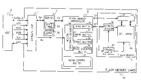
FIG. 1 is a block diagram showing data exchanges between a
flash memory card 10 according to Embodiment 1 of the present
invention and a host H;
FIG. 2 is a schematic diagram showing the structure of a cell
array 4b inside a flash memory 4 according to Embodiment 1 of the
present invention;
FIG. 3 is a flow chart about operations of a merge control
section 3f according to Embodiment 1 of the present invention;
FIG. 4 is a flow chart about the first merge process S3, one
of the operations of the merge control section 3f according to
Embodiment 1 of the present invention;
FIG. 5 is a schematic diagram showing changes in the states
of the pages inside the flash memory 4 during the first merge process
S3 according to Embodiment 1 of the present invention;
CA 02452441 2003-12-29
22
FIG. 6 is a flow chart about the second merge process S4,
another of the operations of the merge control section 3f according
to Embodiment 1 of the present invention;
FIG. 7 is a schematic diagram showing changes in the states
of the pages inside the flash memory 4 during the second merge
process S4 according to Embodiment 1 of the present invention;
FIG. 8 is a block diagram showing data exchanges between a
flash memory card 10A according to Embodiment 2 of the present
invention and a host H;
FIG. 9 is a block diagram showing data exchanges between a
flash memory card lOB according to Embodiment 3 of the present
invention and a host H;
FIG. 10 is a block diagram showing an example of data exchanges
between a conventional flash memory card 100 and a host H.
It will be recognized that some or all of the Figures are
schematic representations for purposes of illustration and do not
necessarily depict the actual relative sizes or locations of the
elements shown.
BEST MODE FOR CARRYING OUT THE INVENTION
CA 02452441 2003-12-29
~23
The following explains the best mode for carrying out the
present invention with describing some preferable Embodiments and
referring to the drawings.
(( Embodiment 1 ))
FIG. 1 is a block diagram showing data exchanges between a
flash memory card 10 according to Embodiment 1 of the present
invention and a host H. The flash memory card 10 is connected with
the host H through the following five types of lines. The lines
are composed of nine lines in total; four data lines DATO-3 , a clock
line CLK, a power line VDD, two ground lines VSS1 and VSS2, and
a command line CMD .
A host interface 1 is the circuit for performing
communications directly with the host H through the above-mentioned
nine lines . The host interface 1 receives commands from the host
H through the command line CMD and decodes the commands . After that ,
the host interface performs, for example, the following operations
in response to the commands . When a command from the host H is a
read command, the host interface 1 decodes the command into the
logical address AL of the read target and sends the address to a
flash memory controller 3. When a command from the host H is a write
command, the host interface 1 decodes the command into the logical
address AL of the write target and sends the address to the flash
memory controller 3. On the other hand, the host interface 1 reads
CA 02452441 2003-12-29
' 24
data objects to be written from the data lines DATO-3 in
synchronization with a transfer clock received from the clock line
CLK, and stores the data ob jects in the buffer 2 . When a command
from the host H is an erase command, the host interface 1 decodes
the command into the logical address AL of the erase target and
sends the address to the flash memory controller 3.
The buffer 2 is an SRAM preferably, and temporarily stores
the data objects Da exchanged between the host interface 1 and the
flash memory controller 3. Thereby, the host interface 1 and the
flash memory controller 3 can exchange data objects Da with each
other without obstructed by a difference in operating speeds, that
is , a difference in frequency between the transfer clock CLK from
the host H and the internal clock of the flash memory card 10. In
addition, the buffer 2 provides the host interface 1 and the flash
memory controller 3 with respective working memory spaces.
Flash memories 4 are NAND-type EEPROM (electrically erasable
programmable ROM) preferably, and include a page buffer 4a, a cell
array 4b, an address decoder 4c, and an erasing circuit 4d.
FIG. 2 is a schematic diagram showing the structure of the
cell array 4b. The cell array 4b is an assembly of a plurality of
the physical blocks BO , B1, B2 , ... Each of the physical blocks is
the following two-dimensional arrangement of many memory cells:
eight memory cells connected in the NAND type compose one line,
CA 02452441 2003-12-29
'25
and 512 lines compose one page. Furthermore, a redundant area
composed of 16 lines is added to every one page. The arrangement
of one page with the addition of the redundant area composes one
unit, and 32 units compose one physical block. For example, the
first physical block BO includes 32 pages PO-P31. The redundant
areas Pr0-Pr31 of 16 bytes each are added to the respective pages
PO-P31. Similarly, the second physical block B1 includes 32 pages
QO-Q31 , and the redundant areas Qr0-Qr31 are added to the respective
pages QO-Q31. Likewise other of the physical blocks B2, B3, ...
Since one memory cell stores one bit data, in the cell array
4b, 8 bits = 1 byte are stored per one line, 512 bytes per one page,
and 512 bytes X 32 = l6kB per one physical block. Furthermore,
in Embodiment 1, the cell array 4b comprises 21° = 1024 of the physical
blocks, thus comprising the storage capacity of l6kB X 1024 = 16MB.
The flash memory 4 comprises, for example, two page buffers
4a. Each of the page buffers 4a can store one-page data. When data
is written into the cell array 4b, data items Da from the flash
memory controller 3, in groups of 2 X 512 bytes, are temporarily
stored in the two page buffers 4a. Furthermore, the data items are
written in parallel from the respective page buffers 4a onto two
separate pages in the cell array 4b. When data is read from the
cell array 4b, data items are read in parallel from two separate
pages inside the cell array 4b, and temporarily stored in the two
respective page buffers 4a. Furthermore, the data items are
CA 02452441 2003-12-29
' 26
transferred in parallel from the two page buffers 4a to the flash
memory controller 3 as a series of data Da.
Two target pages of writing or reading are selected from
separate physical blocks. For example, the two pages hatched in
FIG. 2, that is, the first pages PO and QO of the first physical
block BO and the second physical block B1, respectively, are
selected. Similarly, from one of the odd-numbered physical blocks
and one of the even-numbered physical blocks , the respective pages
at corresponding positions are selected. At that time, the address
decoder 4c performs the selection according to the physical address
AP received from the flash memory controller 3. The two-page pair
inside the cell array 4b selected in such a manner is hereafter
referred to as one area.
The erasing circuit 4d applies a high voltage across the
physical block corresponding to the physical address AP received
from the flash memory controller 3 , thereby collectively erasing
data stored inside the physical block. In order to perform the data
erasing separately in each of the physical blocks at that time,
the physical blocks inside the cell array 4b are electrically
insulated from each other.
The flash memory controller 3 performs data input/output
control over the flash memory 4 using the components described as
follows .
CA 02452441 2003-12-29
27
An address conversion section 3a receives a logical address
AL from the host interface 1. Furthermore, the section selects the
area corresponding to the logical address AL from the inside of
the cell array 4b of the flash memory 4, and converts the logical
address AL into the physical address AP of the area. The address
conversion section 3a assigns generally more than one physical
address AP of area to one logical address AL. Furthermore, the
section classifies a plurality of the areas corresponding to the
same logical address AL into three states, namely, blank, enabled,
and disabled states , and selects the physical addresses AP of the
areas according to the respective states.
The blank state represents that data has not yet been written
in the area after the erasure of data. On the other hand, the enabled
and disabled states are the states of the area in which data is
written. The enabled and disabled states represent that the read
section 3b is allowed to read and prohibited from reading data from
the area, respectively.
Information about the state of each area is stored in the
redundant area added to each page of the flash memory 4 (such as
the redundant area Pr0 corresponding to the page PO ) . In particular,
the common information about the state of the area is stored in
the redundant areas of the pages belonging to the same area.
The address conversion section 3, at startup of the flash
CA 02452441 2003-12-29
'28
memory card 10 , checks the states of all the areas inside the cell
array 4b of the flash memory 4. Furthermore, the section creates,
inside the buffer 2, a table 2a regarding the state of each of the
areas (which is hereafter referred to as a state table) . The state
table 2a is , for example, a list of the physical addresses of areas ,
the logical addresses corresponding to the areas, and the
information about the states of the areas.
When a logical address AL shows a target of reading data,
the address conversion section 3a consults the state table 2a,
thereby selecting an enabled area from among the areas inside the
cell array 4b corresponding to the logical address AL. The read
section 3b sends the physical address AP of the enabled area to
the flash memory 4. The address decoder 4c decodes the physical
address AP entered into the flash memory 4. Thereby, data items
are read in parallel from the respective pages belonging to the
area inside the cell array 4b corresponding to the physical address
AP into the two page buffers 4a. The read section 3b transfers the
data items Da from the page buffers 4a to the buffer 2.
When a logical address AL shows a target of writing data,
the address conversion section 3a consults the state table 2a,
thereby selecting blank areas from the inside of the cell array
4b. Furthermore, the section assigns the physical addresses AP of
the blank areas to the logical address AL of the write target . The
write section 3c transfers the data objects Da to be written, in
CA 02452441 2003-12-29
29
groups of 2X512 bytes, from the buffer 2 to the page buffers 4a
inside the flash memory 4 . In conjunction with that , the section
sends the physical address AP of the blank area selected by the
address conversion section 3a to the flash memory 4. The address
decoder 4c decodes the physical address AP entered in the flash
memory 4. Thereby, data items are written in parallel from the
different page buffers 4a onto the respective pages belonging to
the area inside the cell array 4b corresponding to the physical
address AP. Furthermore, at the end of the data writing, the address
conversion section 3 updates the state table 2a and rewrites the
item regarding the state of the write target area from "blank" to
"enabled".
As described above , the writing and reading of data into and
from the flash memory 4 are performed through the two page buffers
4a on an area-by-area basis, that is, one page each of the two
separate physical blocks in parallel . Thus , the flash memory card
10 according to Embodiment 1 shortens the writing and reading
durations for the flash memory 4.
When a logical address AL shows a target of erasing data,
the address conversion section 3a identifies the physical address
AP of the physical block corresponding to the logical address AL.
An erase section 3d sends the physical address AP of the erasing
target identified by the address conversion section 3a to the
erasing circuit 4d inside the flash memory 4. The erasing circuit
CA 02452441 2003-12-29
4d stops the address decoder 4c, and applies a predetermined high
voltage across the physical block corresponding to the received
physical address AP, thereby performing the erasing of data for
the physical block. Furthermore, at the end of the data erasing,
5 the address conversion section 3 updates the state table 2a and
rewrites "enabled" into the items regarding the states of all the
areas inside the physical block of the erasing target.
At the time of the data writing, the address conversion
section 3a consults the state table 2a along with the
10 above-described operations, and retrieves an enabled area among
the areas of the physical addresses corresponding to the logical
address AL of the write target . When the writing requested by the
host H is the overwriting of data, generally an enabled area exists
in the areas of the physical addresses corresponding to the logical
15 address AL. Then, a page-disabling section 3e disables the enabled
area as described bellow. Furthermore, the address conversion
section 3 updates the state table 2a, and rewrites the item regarding
the state of the area from "enabled" to "disabled. " Thereby, the
read section 3b is prohibited from accessing to the area.
20 The page-disabling section 3e rewrites data inside the
redundant area corresponding to the enabled page, thereby disabling
the page. For example, it is defined that a page is enabled and
disabled when the predetermined one bit (flag) inside the redundant
area is "1" and "0," respectively. Since the flag corresponding
CA 02452441 2003-12-29
~3L
to the enabled page is "1, " the page-disabling section 3e changes
the flag from "1" to "0," in other words, writes "0" into the flag
inside the redundant area, thereby disabling the page.
As described above, the flash memory card 10 according to
Embodiment 1, when requested the overwriting of data by the host
H, writes new data in another area without erasing the original
data. Furthermore, the card assigns the physical address of the
area in which the new data is written to the logical address of
the write target . In addition, the card disables states of the areas
at the other physical addresses corresponding to the logical address .
Thereby, when receiving from the host a read command aimed at the
logical address, the read section 3b can access only the area storing
the latest data items among a plurality of the areas corresponding
to the logical address . Thus , the overwriting of data at the same
logical address is realized without entailing an erasure of data
in the flash memory 4. Therefore, the overwriting duration
shortens by the erasing duration.
The flash memory card 10 according to Embodiment 1 further
comprises a merge control section 3f inside the flash memory
controller 3. As described above, the overwriting of data produces
disabled pages . Accordingly, the rate of the disabled areas to the
enabled areas increases when the overwriting of data is repeated.
The merge control section 3f controls the read section 3b, the write
section 3c, the erase section 3d, and the page-disabling section
CA 02452441 2003-12-29
32
3e as follows, thereby copying data on the enabled pages inside
a predetermined physical block onto the blank pages inside other
physical blocks. Furthermore, the merge control section erases the
original data in the physical block, thereby increasing the number
of the physical blocks including only blank pages (the blank
physical blocks). As a result, the rate of the disabled areas to
the enabled areas can be reduced.
FIG. 3 is a flow chart about the operation of the merge control
section 3f.
The merge control section 3f starts up at the time of writing
of data into the flash memory 4.
Step S1:
The merge control section 3f consults the state table 2a
inside the buffer 2 and counts the number N of the blank physical
blocks.
Step S2:
The number N of the blank physical blocks counted in Steg
S1 is compared with each of the first threshold value thl and the
second threshold value th2. Here, the first threshold value thl
and the second threshold value th2 are , for example , equal to about
CA 02452441 2003-12-29
33
50~ and about 20~ of the number of all the physical blocks inside
the cell array 4b, respectively. Furthermore, the merge control
section 3f causes the process to branch as follows, depending on
the result of comparison : ( 1 ) The merge control section 3f stops
when the number N of the blank physical blocks is equal to or more
than the first threshold value thl (N~thl ) . ( 2 ) The merge control
section 3f performs the first merge process S3 when the number N
of the blank physical blocks is smaller than the first threshold
value thl and equal to or more than the second threshold value th2
( th2SN<thl ) . ( 3 ) The merge control section 3f performs the second
merge process S4 when the number N of the blank physical blocks
is smaller than the second threshold value th2 (N<th2).
Through Step S1 and Step S2, the merge control section 3f
performs the following merge process only when the number N of the
blank physical blocks is smaller than the first threshold value
thl, in other words, only when the remaining area available for
the data writing is small . Thus , the flash memory card 10 according
to Embodiment 1 limits the extension of the writing duration due
to the merge process.
<The first merge process S3>
FIG. 4 is a flow chart about the first merge process S3. FIG.
5 is a schematic diagram showing changes in the states of the pages
inside the cell array 4b during the first merge process S3. In
CA 02452441 2003-12-29
34
Embodiment 1, the corresponding pages in one of the odd-numbered
physical blocks and one of the even-numbered physical blocks belong
to the same area. Furthermore, the data input/output operations
are performed area by area in parallel. Accordingly, the changes
in states of pages are substantially common between the odd-numbered
physical blocks and the even-numbered physical blocks. Therefore,
FIG. 5 shows only the odd-numbered physical blocks inside the cell
array 4b.
FIG. 5 represents the data items stored in the respective
areas PO , P1, P2 , ... as the reference symbols DO , D1, D2 , ... written
inside the boxes showing the respective areas. In addition, the
states of the areas are represented as the numerals 1 and 0 written
inside the boxes showing the corresponding redundant areas PrO,
Prl , Pr2 , ... Here , the numerals 1 and 0 show the enabled and disabled
states, respectively. Furthermore, the states of the areas are
blank when the boxes showing the areas are blank.
Substep S31:
As shown in ( a) of FIG. 5 , new data items ( for example, dl ,
d2, and d3) are written into the blank areas. Then, the merge
control section 3f obtains the number k (for example, 3) of the
blank areas in which the new data items are written.
Substep 532:
CA 02452441 2003-12-29
The merge control section 3f consults an address table 2b
inside the buffer 2 , and selects the physical block BL as a source
of copying in decreasing order of the number of the disabled areas ,
the physical block including the largest number of the disabled
5 areas first. Here, the address table 2b is a list of the addresses
of the physical blocks and the numbers of the disabled pages
belonging to the physical blocks. For example, the top physical
block BL is selected as the source physical block in (a) of FIG.
5.
10 Substep S33:
The merge control section 3f consults the state table 2a
inside the buffer 2, and selects the same number of the enabled
areas of the source physical block BL as the number of the areas
obtained in Substep 531, that is, k areas in order, the top area
15 PO first . For example, the three enabled areas PO , P1, and P3 are
selected in (a) of FIG. 5. Here, when the number of the enabled
areas inside the source physical block BL is smaller than k, Substep
S32 is performed again, and thereby another physical block is
selected as a source physical block and the rest of the enabled
20 areas are selected from the physical block.
Substep S34:
The merge control section 3f consults the state table 2a
CA 02452441 2003-12-29
36
inside the buffer 2 and selects the same number of blank areas as
the number of the areas obtained in Substep 531, that is, k areas
from a physical block different from the source physical block BL.
For example , the three blank areas CPO , CP1, and CP3 are selected
in (a) of FIG. 5.
Substep 535:
The merge control section 3f reads data items from the enabled
areas selected in Substep S33 using the read section 3b. The data
items read are temporarily stored in the buffer 2. Furthermore,
the merge control section 3f writes the data items temporarily
stored in the buffer 2 into the respective blank areas selected
in Substep S34 using the write section 3c . Thus , data items on the
k enabled areas inside the source physical block BL are copied into
the respective blank areas of the other physical blocks. For
example , the data items DO , D1, and D3 in the three enabled areas
PO , P1, and P3 inside the source physical block BL are copied into
the three blank areas CPO, CP1, and CP3, respectively, in (a) of
FIG. 5.
Substep 536:
The merge control section 3f disables the k enabled areas
inside the source physical block BL using the page-disabling section
3e . In ( b ) of FIG. 5 , for example , data in the redundant areas Pr0 ,
CA 02452441 2003-12-29
~37
Prl , and Pr3 corresponding to the three enabled areas PO , P1, and
P3 inside the source physical block BL is changed from "1" to "0."
Furthermore, the merge control section 3f updates the state table
2a inside the buffer 2, and rewrites the items regarding the states
of the k enabled areas inside the source physical block BL from
"enabled" to "disabled." In conjunction with that, the merge
control section 3f updates the address table 2b inside the buffer
2 based on the state table 2a updated.
Substep S37:
The merge control section 3f consults the state table 2a
inside the buffer 2 and selects the physical block including only
disabled areas, or alternatively, only a large number of disabled
areas and a small number of blank areas , and assigns the physical
block as an erasing target physical block BE. In (c) of FIG. 5,
for example, the top physical block BE is selected as an erasing
target since the states of all the areas inside the physical block
BE axe disabled.
Substep S38:
It is checked whether an erasing target physical block BE
can be selected in Substep S37. The merge control section 3f causes
the process to branch to Substep S39 when an erasing target physical
block BE exists , and finishes the first merge process S3 at other
CA 02452441 2003-12-29
38
times.
Substep S39:
The merge control section 3f performs the erasing of data
for the erasing target physical block BE using the erase section
3d. In (d) of FIG. 5, for example, all the boxes showing the areas
inside the erasing target physical block BE are drawn as blank boxes
so as to represent that the states of all the areas are changed
into blank states. After the end of the data erasing, the merge
control section 3f updates the state table 2a inside the buffer
2, and rewrites "enabled" into the items regarding the states of
all the areas of the erasing target physical block BE. In
conjunction with that, the merge control section 3f updates the
address table 2b inside the buffer 2 based on the state table 2a
updated. Then, the merge control section 3f repeats the process
from Substep S37.
As described above, the first merge process S3 is performed
at every time of the data writing when the number N of the blank
physical blocks is smaller than the first threshold value thl.
Generally the amounts of the data objects to be written are equal
to the storage capacity on the order of the integral multiple of
the physical block. On the other hand, in Substep 533, the merge
control section 3f selects enabled areas as many as the areas in
which new data is written. Accordingly, generally the number of
CA 02452441 2003-12-29
-3 9
the physical blocks that become erasable through the first merge
process S3 can be adjusted on the order of the number of the blank
physical blocks consumed by the writing of new data, especially
when data is overwritten into the same logical address . As a result ,
the flash memory card 10 according to Embodiment 1 can suppress
an increase in the rate of the disabled areas to the enabled areas
at the time of the repetition of the overwriting of data.
<The second merge process S4>
FIG. 6 is a flow chart about the second merge process S4.
FIG. 7 is a schematic diagram showing changes in the states of the
pages inside the cell array 4b during the second merge process S4.
FIG. 7 shows only the odd-numbered physical blocks inside the cell
array 4b in a manner similar to FIG. 5. Furthermore, data items
stored in the areas and the states of the areas are shown as reference
symbols similar to those shown in FIG. 5.
Substep 541:
The merge control section 3f prohibits the write section 3c
from writing new data in contrast to the time of the first merge
process S3.
Substep S42:
CA 02452441 2003-12-29
~40
The merge control section 3f consults the address table 2b
inside the buffer 2 and selects the source physical block BL in
decreasing order of the number of the disabled areas , the physical
block including the largest number of the disabled areas first,
in a manner similar to Substep S32 of the first merge process S3.
In ( a ) of FIG . 7 , for example , the top physical block BL is selected
as the source physical block.
Substep S43:
The merge control section 3f consults the state table 2a
inside the buffer 2 and selects all the enabled areas inside the
source physical block BL. In (a) of FIG. 7, for example, all the
enabled areas PO and P3 inside the physical block BL are selected.
Substep S44:
The merge control section 3f consults the state table 2a
inside the buffer 2 and selects blank areas as many as the enabled
areas selected in Substep S43 from a physical block different from
the source physical block BL. In (a) of FIG. 7, for example, the
top two areas CPO and CP1 inside the one Bn of the blank physical
blocks are selected.
Substep S45:
CA 02452441 2003-12-29
'41
The merge control section 3f reads data items from the enabled
areas selected in Substep S43 using the read section 3b. The data
items read are temporarily stored in the buffer 2. Furthermore,
the merge control section 3f writes the data items temporarily
stored in the buffer 2 into the respective blank areas selected
in Substep S44 using the write section 3c. Thus, the data items
in all the enabled areas inside the source physical block BL are
copied into the respective blank areas of another physical block.
In ( a ) of FIG . 7 , for example , the data items DO and D3 in the enabled
areas PO and P3 inside the source physical block BL are copied into
the two blank areas CPO and CP1 of the blank physical block Bn,
respectively.
Substep S46:
The merge control section 3f selects the source physical
block BL as an erasing target physical block BE as shown in (b)
of FIG. 7. Furthermore, the section performs the erasing of data
for the erasing target physical block BE using the erase section
3d. In ( c ) of FIG. 7 , for example , all the boxes showing the areas
inside the erasing target physical block BE are drawn as blank boxes
so as to represent that the states of all the areas are changed
into blank states. After the end of the data erasing, the merge
control section 3f updates the state table 2a inside the buffer
2 and rewrites "enabled" into the items regarding the states of
all the areas inside the erasing target physical block BE. In
CA 02452441 2003-12-29
a 42
conjunction with that, the merge control section 3f updates the
address table 2b inside the buffer 2 based on the state table 2a
updated.
As described above, the second merge process S4 is performed
when the number N of the blank physical blocks is smaller than the
second threshold value th2 . At that time , the writing of new data
is prohibited, and the producing of an increase in the number N
of the blank physical blocks through Substeps S42-S46 is placed
on a higher priority. Thereby, the rate of the disabled areas to
the enabled areas is reduced so that the number N of the blank
physical blocks is secured at or beyond the second threshold value
th2. As a result, the flash memory card 10 according to Embodiment
1 increases the amounts of data that can be stored therein.
The flash memory 4 comprises the two page buffers 4a in
Embodiment 1. Alternatively, the flash memory may comprise only
one page buffer, or three or more of the page buffers.
(( Embodiment 2 ))
FIG. 8 is a block diagram showing data exchanges between a
flash memory card 10A according to Embodiment 2 of the present
invention and a host H. The flash memory card 10A according to
Embodiment 2 comprises two flash memories in contrast to the
counterpart 10 of Embodiment 1 (FIG. 1). In FIG. 8, components
CA 02452441 2003-12-29
'4 3
similar to those of Embodiment 1 are marked with the same reference
symbols as those of Embodiment 1. Furthermore , the description of
Embodiment 1 is cited regarding those similar components.
A flash memory controller 3A and two flash memories 4A and
4B according to Embodiment 2 are really similar in internal
structure to their respective counterparts 3 and 4 of Embodiment
1, and therefore FIG. 1 is cited regarding them.
The duration of data transfer between the flash memory
controller 3A and the flash memory 4A or 4B inside the page buffers
4a is on the order of several tens of nsec. On the other hand, the
duration of writing data from the page buffer 4a into the cell array
4b is on the order of several hundreds of nsec . Using the difference
between those processing times, the flash memory controller 3A
according to Embodiment 2 performs a writing operation of data into
one of the flash memories and a merge process in the other of the
flash memories in parallel as described bellow. Thereby, the
extension of the writing duration due to the merge process can be
reduced compared with that of the flash memory card 10 according
to Embodiment 1.
For example, when writing data into the first flash memory
4A, a write section 3c inside the flash memory controller 3A
transfers the data object Da to be written into the first flash
memory 4A area by area, in a manner similar to that of Embodiment
CA 02452441 2003-12-29
'44
1 . The merge control section 3f inside the flash memory controller
3A, at every time of the transfer of the one area, starts up and
performs Step S1 and Step S2 for the second flash memory 4B in a
manner similar to that of Embodiment 1. The merge control section
3f further performs the first merge process S3 or the second merge
process S4 according to the result of the comparison in Step S2,
in a manner similar to that of Embodiment 1.
<The first merge process S3>
In the first merge process S3 according to Embodiment 2, in
contrast to that of Embodiment 1, the merge control section 3f
obtains in Substep S31 the number of the areas in which new data
is written inside the first flash memory 4A. In Substep 533, enabled
areas as many as the areas in which new data is written inside the
first flash memory 4A are selected from the source physical block
inside the second flash memory 4B. Thereby, one area of the second
flash memory 4B a.s copied into another area in parallel with the
writing of data in one area into the first flash memory 4A.
Furthermore, the number of the target areas of the first merge
process S3 in the second flash memory 4B is equal to the number
of the write target areas in the first flash memory 4A. Accordingly,
the duration required of the first merge process S3 in the second
flash memory 4B is nearly equal to the writing duration in the first
flash memory 4A. As a result of the above-described operations,
the extension of the writing duration due to the first merge process
CA 02452441 2003-12-29
S3 can be reduced in Embodiment 2 , compared with that in Embodiment
1.
<The second merge process S4>
In the second merge process S4 according to Embodiment 2,
in contrast to that of Embodiment 1, the merge control section 3f
allows the data writing into the first flash memory 4A. Thereby,
the data writing into the first flash memory 4A can be performed
in parallel with the second merge process S4 in the second flash
memory 4B. Therefore, the extension of the writing duration due
to the second merge process S4 can be reduced in Embodiment 2,
compared with that in Embodiment 1.
~~ Embodiment 3 ))
FIG. 9 is a block diagram showing data exchanges between a
flash memory card lOB according to Embodiment 3 of the present
invention and a host H. The flash memory card 10B according to
Embodiment 3 comprises two flash memories in a manner similar to
the counterpart 10A of Embodiment 2 (FIG. 8) . In FIG. 9, components
similar to those of Embodiment 1 are marked with the same reference
symbols as those of Embodiment 1. Furthermore, the description of
Embodiment 1 is cited regarding those similar components.
The two flash memories 4A and 4B according to Embodiment 3
CA 02452441 2003-12-29
46
are really similar in internal structure to their counterpart 4
of Embodiment 1, and therefore FIG. 1 is cited regarding them.
A flash memory controller 3B according to Embodiment 3
substantially includes two internal structures each of which is
similar to that of its counterpart 3 according to Embodiment 1.
Of the internal structures similar to that of the flash memory
controller 3 according to Embodiment 1, the one is connected to
the first flash memory 4A, and separately the other is connected
to the second flash memories 4B. Furthermore, the internal
structures are separately connected to the buffer 2B through the
separate data buses . Because of such composition, the flash memory
card lOB according to Embodiment 3 can perform the writing operation
and the merge process in parallel for the two flash memories 4A
and 4B in a manner similar to that of Embodiment 2. In contrast
to Embodiment 2, in particular, data transmissions between the
buffer 2B and the flash memory controller 3B and data transmissions
between the flash memory controller 3B and the flash memories 4A
and 4B are also performed in parallel. Accordingly, the writing
duration can further shorten by the data transfer duration compared
with that of Embodiment 2.
As described above, the flash memory system according to the
present invention can copy data on the enabled pages inside a
predetermined physical block into other physical blocks.
Furthermore, at the end of the copying of data on all the enabled
CA 02452441 2003-12-29
47
pages inside the predetermined physical block, the system can erase
collectively data in the physical block. Through such a merge
process , the flash memory system according to the present invention
can erase data on the disabled pages inside the physical block
including enabled pages, in contrast to conventional systems.
Accordingly, the flash memory system according to the present
invention can reduce the rate of the disabled pages to the enabled
pages. As a result, the amount of data that can be stored at the
time of the repetition of the overwriting of data is larger than
those of the conventional systems.
The flash memory system according to the present invention
may further perform the above-described merge process when new data
is written therein and the number of blank physical blocks is smaller
than the first threshold value. Thus, the above-described flash
memory system can reduce the extension of the writing duration due
to the copying of data by the restriction of the execution timing
of the merge process.
The flash memory system according to the present invention
may adjust the number of the source pages to be equal to or more
than the number of the pages on which new data is written. Thereby,
when data is overwritten at the same logical address, the system
can adjust the number of the physical blocks erased in the
above-described merge process to be on or beyond the order of the
number of the blank physical blocks consumed by the writing of new
CA 02452441 2003-12-29
. 48
data. As a result, the system can avoid an increase in the rate
of the disabled pages to the enabled pages at the time of the
repetition of the overwriting of data. Therefore, the system can
increase the amounts of data that can be stored.
The flash memory system according to the present invention
may provide the above-described merge process with a higher priority
than the writing operation of new data when the number of the blank
physical blocks is smaller than the second threshold value.
Thereby, the system can reduce the rate of the disabled pages to
the enabled pages so as to secure the number of the blank physical
blocks on or beyond the order of the second threshold value. As
a result, the system can increase the amounts of data that can be
stored.
The second threshold value is smaller than the first
threshold value when the above-described flash memory system
performs both of the operation in the case of the number of the
blank physical blocks equal to or smaller than the first threshold
value and the operation in the case of the number equal to or smaller
than the second threshold value. Thereby, the merge process does
not take precedence over the writing operation of new data until
the blank physical blocks are too small in number to allow the
writing of new data therein. As a result, the extension of the
writing duration due to the merge process can be reduced.
CA 02452441 2003-12-29
~49
The flash memory system according to the present invention
may comprise a list of the addresses of the physical blocks and
the numbers of the disabled pages belonging to the physical blocks .
The above-mentioned list is consulted at the time of the selection
of the source physical block in the above-described merge process .
Thereby, the source physical block is selected easily and quickly
in decreasing order of the number of the disabled areas , the physical
block including the largest number of the disabled areas first.
As a result , the time required to the above-described merge process
shortens since the number of the enabled pages targeted for the
above-described merge process is minimized.
The above-described disclosure of the invention in terms of
the presently preferred embodiments is not to be interpreted as
intended for limiting. Various alterations and modifications will
no doubt become apparent to those skilled in the art to which the
invention pertains, after having read the disclosure. As a
corollary to that, such alterations and modifications apparently
fall within the true spirit and scope of the invention. Furthermore,
it is to be understood that the appended claims be intended as
covering the alterations and modifications.
INDUSTRIAL APPLICABILITY
According to the present invention , for flash memories , the
per-physical-block rate of the disabled pages to the enabled pages
CA 02452441 2003-12-29
~50
can be maintained low enough. Thereby, a substantial increase in
the storage capacity can be achieved for the flash memories.
Therefore, the industrial applicability in the present invention
is very high.