Note: Descriptions are shown in the official language in which they were submitted.
CA 02452739 2003-12-09
2002P18560US-RAI
Patent-Treuhand-Gesellschaft
fur elektrische Gliihlampen mbH., Munich
Title
Switched-mode power supply
E'ield of the invention
The invention relates to a switched-mode power supply
according to the preamble of claim 1. Switched-mode
power supplies are referred to below as power supply
for short. The invention essentially relates to a power
supply with a switching snubber device. The power
supply is suitable for operating light sources.
Background of the invention
Power supplies, such as are known, for example, from
Mohan, Undeland, Robins: "Power Electronics", John
Wiley & Sons, 1995, New York, USA, Chapters 7 and 10
have at least one electronic switch. When these
switches are operated, switching losses occur which can
be reduced by switching snubber devices. An overview of
such switching snubber devices is given, for example,
in the following text: Philip C. Todd: "Snubber
Circuits: Theory, Design and Application" in the Power
Supply Design Seminar Manual, UNITRODE, Merrimack, NH,
USA, 1993. There, the differences between dissipative
and non-dissipative switching snubber devices are
described.
Dissipative switching snubber devices can be realized
with little outlay. However, they do have the
disadvantage that they may result in high losses and
high parasitic oscillations. The losses reduce the
CA 02452739 2003-12-09
efficiency of the switched-mode power supply, and the
parasitic oscillations cause radio interference.
A non-dissipative snubber circuit for a DC chopper
controller is described in the publication EP 0 798 857
(Osterried). This circuit contains at least 2 diodes
and an inductor. In particular, the inductor entails
considerable outlay for realizing the snubber circuit.
Summary of the invention
The object of the present invention is to provide a
power supply which has a switching snubber device which
can be realized with little outlay, produces a low
power loss and excites few parasitic oscillations.
This object is achieved by a power supply having the
following features:
A first and a second energy feed point,
~ a transformer having a primary and a secondary
winding, it being possible for the secondary
winding to be connected to a load,
~ a first electronic switch which is connected in
series with the primary winding,
~ the series circuit of the first electronic
switch and the primary winding is coupled to
the first and the second energy feed point,
~ a switching snubber device which is connected
in parallel with the primary winding or in
parallel with the first electronic switch and
which contains the series circuit of a
capacitor and a second electronic switch,
~ the series circuit of the capacitor and the
second electronic switch causes the energy,
which is represented by the current in the
primary winding when the first electronic
switch is switched off, to be at least
partially absorbed by the capacitor,
CA 02452739 2003-12-09
~ the second electronic switch causes a
substantial part of the energy absorbed by the
capacitor to be fed back into the transformer.
The invention is based on a power supply having a
transformer which has a primary and a secondary
winding. The secondary winding can be connected to a
load. The transformer may have two or more secondary
windings, it being possible for each secondary winding
to be connected to in each case one load.
In general, each electrical consumer may represent a
load. However, the invention is suitable, in
particular, for transforming a mains voltage of, for
example, 230 Veff into a DC or AC voltage of less than
50 V. It is thus possible to operate electronic
appliances, for example.
Owing to the stringent requirements in terms of power
loss and radio interference in lighting engineering,
the invention is particularly suitable for operating
light sources. Incandescent lamps, light-emitting
diodes or so-called OLEDs (Organic Light Emission
Devices) may be used in this case, for example. When
operating light-emitting diodes it is advantageous to
rectify and smooth the AC voltage provided across the
secondary winding.
In addition, the invention is based on the assumption
that the power supply has a first and a second energy
feed point. These energy feed points are provided for
feeding a DC supply voltage. The DC supply voltage may
be provided, for example, by a battery or by
rectification and smoothing of a mains voltage.
In addition, the invention is based on the assumption
that a first electronic switch is connected in series
with the primary winding. The resultant series circuit
CA 02452739 2003-12-09
- 4 -
is coupled to the first and the second energy feed
point. If the first electronic switch is closed, the DC
supply voltage causes the current in the primary
winding to increase. This principle is realized in many
topologies for switched-mode power supplies. These are
described in the abovementioned text (~ohan, Undeland,
Robins: ~~Power Electronics", John Wiley & Sons, 1995,
New York, USA, Chapters 7 and 10). The so-called
flyback converter is in common use, since this topology
can be realized in a cost-effective manner at low power
(up to 100 W).
After a predetermined time, the first electronic switch
is switched off again. This switching-off operation
prevents the current built up in the primary winding
from continuing to flow through the first electronic
switch. If no switching snubber device is provided, a
high voltage builds up across the working terminals of
the first electronic switch and results in high losses
in the first electronic switch and may lead to the
switch being destroyed.
In addition, the invention is based on the assumption
that the power supply contains a switching snubber
device. The switching snubber device contains at least
the series circuit of a capacitor and a second
electronic switch.
In addition, the invention is based on the assumption
that the switching snubber device is connected into the
power supply such that the energy, which is represented
by the current in the primary winding when the first
electronic switch is switched off, is at least
partially absorbed by the capacitor.
Since, in the prior art, the second electronic switch
is in the form of a fast diode, the energy absorbed by
the capacitor can no longer flow away via the second
CA 02452739 2003-12-09
. 5 .
electronic switch. Care must therefore be taken in the
prior art to ensure that the capacitor is discharged
before the switch is switched off again. This takes
place in the prior art by means of a first resistor
which provides a discharge current path for the
capacitor. The energy stored in the capacitor is
converted in the first resistor into lost power. If a
high value is selected for the first resistor,
oscillations in the voltage present across the working
terminals of the first electronic switch result. These
oscillations may cause radio interference.
As described above, a fast diode is used for the second
electronic switch in the prior art. The response time
of a diode is generally described by a reverse recovery
time. If, after a period of time for which a current is
flowing through the diode in the forward direction, the
direction of the current is reversed, during the
reverse recovery time a current flows in the reverse
direction through the diode. The reverse recovery time
in diodes according to the prior art is so short that
the capacitor may be discharged to only an
insignificant extent during the reverse recovery time.
According to the invention, the second electronic
switch causes a substantial part of the energy absorbed
by the capacitor to be fed back into the transformer.
Once the energy, which is represented by the current in
the primary winding of the transformer when the first
electronic switch is switched off, has been dissipated,
the current in the primary winding, which previously
flowed in a positive direction, is reduced to zero. A
diode according to the prior art prevents the current
in the negative direction from being increased. A
second electronic switch according to the invention
allows a current to flow in the negative direction.
This is the case until the energy stored in the
CA 02452739 2003-12-09
- 6 -
capacitor in the form of a current in the primary
winding has been fed back into the transformer. A large
proportion of the energy fed back is output by the
transformer via its secondary winding to the load.
Advantageously, only a little power loss is thus
produced in the power supply.
Also of advantage is the fact that the resonant
circuit, formed by the primary winding and the
capacitor, is damped by the load. This suppresses
parasitic oscillations.
Brief description of the drawings
The invention will be explained in more detail below
using exemplary embodiments and with reference to
drawings, in which:
figure 1 shows an exemplary embodiment according to
the invention of a power supply,
figure 2 shows the time profile of the voltage across
the working terminals of the first electronic
switch according to the prior art,
figure 3 shows the time profile according to the
invention of the voltage across the working
terminals of the first electronic switch,
figure 4 shows a further exemplary embodiment
according to the invention of a power supply,
and
figure 5 shows a further exemplary embodiment
according to the invention of a power supply.
In the text below, resistors are denoted by the letter
R, transistors by the letter T, diodes by the letter D,
CA 02452739 2003-12-09
capacitors by the letter C, in each case followed by a
numeral. In addition, in the text which follows, the
same elements, and elements having the same function,
of the different exemplary embodiments are provided
with the same reference symbols throughout.
Preferred embodiment of the invention
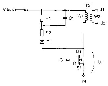
Figure 1 shows an exemplary embodiment according to the
invention of a power supply. A DC supply voltage can be
connected to a terminal Vbus with respect to a
reference potential M. The series circuit of the
primary winding w1 of a transformer TXl and a first
electronic switch, which is in the form of an N-channel
MOSFET T1, is connected between the terminal Vbus and
the reference potential M. Other electronic switches
may also be used, such as, for example, IGBTs, bipolar
transistors or P-channel MOSFETs. The drain terminal Dl
of T1 forms a working terminal of T1 and is connected
to the primary winding W1. The source terminal Sl of T1
is connected to the reference potential M. The gate
terminal Gl of T1 is connected to a control circuit
(not shown). The control circuit ensures that T1 is
switched on and off according to the requirements for
the power supply.
The series circuit of T1 and the primary winding W1 is
selected such that Tl is connected to the reference
potential M. This has the advantage that the control
circuit needs to provide a signal which is also based
on the reference potential M. The outlay for the
control circuit may thus be kept low. It is, however,
also possible to exchange the primary winding W1 and Tl
in the series circuit such that the primary winding W1
is connected to the reference potential M.
The secondary winding W2 of the transformer TX1 has two
terminals J1 and J2 to which a load can be connected.
CA 02452739 2003-12-09
Connected in parallel with the primary winding W1 is
the series circuit of a first resistor R1, a second
resistor R2 and a second electronic switch. The second
electronic switch is in the form of a diode D1 which is
polarized such that it blocks the flow of current from
the terminal Vbus to the reference potential M.
A capacitor C1 is connected in parallel with the first
resistor Rl.
A voltage between the working terminals of the
transistor UT is marked between the drain terminal Dl
and the source terminal S1.
If T1 is closed, the DC supply voltage results in a
positive current through the primary winding W1. If Tl
is switched off, this current continues to flow through
Dl and charges the capacitor C1 until the current is
reduced to a value of zero. The second resistor R2
limits the current through D1. This may be important
for a cost-effective selection of components. The value
of the second resistor may, however, also be zero.
Since R2 also damps the resonant circuit represented by
the primary winding W1 and Cl, a given limit for
parasitic oscillations may be exceeded when R2 has the
value zero. In this case, the value for R2 needs to be
increased until the given limit for parasitic
oscillations is maintafined.
According to the invention, D1 now has a reverse
recovery time which allows a negative current flow
through the primary winding. The reverse recovery time
is long enough to completely discharge C1. The majority
of the energy stored in C1 is thus output via the
transformer to the load. Only an insignificant fraction
is dissipated in. the first resistor R1. R1 serves
besides the purpose of further damping parasitic
CA 02452739 2003-12-09
_ g _
oscillations which, despite a design of D1 according to
the invention, still occur to a slight extent. The
first resistor R1 may, however, also be dispensed with.
Figure 2 shows the profile of the voltage UT from
figure 1 plotted against time t, but for a design of D1
which corresponds to the prior art. At time t1, T1
switches off and the voltage UT increases rapidly. The
value of the voltage UT is, admittedly, limited by the
switching snubber device, but a parasitic oscillation,
triggered by the switching-off process, can clearly be
seen. Once the parasitic oscillation has decayed, the
voltage UT is adjusted to a value which corresponds to
the sum of the DC supply voltage and the output
voltage, transformed into the primary winding W1,
across the secondary winding W2. During operation on a
mains voltage, this value may be, for example, between
100 V and 350 V. The frequency of the parasitic
oscillation is typically in the MHz range.
At time t2, T1 switches on again and the voltage UT is
reduced again to negligible values. With power supplies
which are suitable for operating light-emitting diodes
on a mains voltage, there is a time interval of 5
microseconds, for example, between times t1 and t2. At
time t3, T1 switches off again and the described
process is repeated cyclically. The cycle time in the
abovementioned application is 8 microseconds, for
example.
Figure 3 shows the profile of the voltage UT from
figure 1 plotted against time t, as is produced when
the reverse recovery time of D1 is designed according
to the invention. The amplitude of the interference
voltage is markedly reduced. Less outlay is thus
required for radio interference. A further advantage,
which cannot be seen in figure 3, is the reduced loss
of power which is dissipated in the first resistor Rl.
~ CA 02452739 2003-12-09
_ 1~ _
A lower limit value for the reverse recovery time of D1
can be seen in figure 2. The reverse recovery time of
D1 needs to be at least as long as the cycle time of
the parasitic oscillation which would result according
to the prior art. With parasitic oscillations in the
MHz range, a minimal reverse recovery time of D1 of one
microsecond results.
Figure 4 shows a further exemplary embodiment according
to the invention of a power supply. In comparison with
figure 1, the second electronic switch in figure 4 is
in the form of a bipolar transistor T2. The switching
snubber device, which is connected in parallel with the
primary winding W1, comprises the capacitor Cl, the
transistor T2 and the resistor R3. The series circuit
of C1 and the collector/emitter path of T2 is connected
in parallel with the primary winding W1. R3 is
connected in parallel with the base/emitter path of T2.
In comparison with figure l, the resistor R1 is not
included in figure 4. The function of the diode D1 is
taken on by the base/collector path of T2. The positive
current of the primary winding Wl is conducted via the
resistor R3 and the base/collector path of T2 once T1
has been switched off, and thus charges Cl. When a
transistor T2 is used, the reverse recovery time of the
diode D1 is represented by its storage time. A
transistor therefore needs to be selected for T2 whose
storage time corresponds to the reverse recovery time
of a diode designed according to the invention. A
negative current in the primary winding W1 may flow
during the storage time of T2. If, instead of a diode
for the second electronic switch, a transistor is used,
the power loss in the second electronic switch is
advantageously reduced. Also of advantage is the fact
that the storage time of T2 can be set by the resistor
R3. It is thus possible to adjust the time for which a
negative current flows through the primary winding W1.
CA 02452739 2003-12-09
- 11 -
It is also possible to use a MOSFET or another
electronic switch instead of the bipolar transistor for
T2. It may be necessary to provide for this switch a
drive circuit which opens and closes the switch at the
required times. The switch needs to be closed when the
first electronic switch is open, and to be opened when
the capacitor C1 is discharged again following the
charging process. The second electronic switch needs,
however, to be opened at the latest when the first
electronic switch is closed again.
Figure 5 shows a further exemplary embodiment according
to the invention of a power supply. In comparison with
figures 1 and 4, the switching snubber device in figure
5 is not connected in parallel with the primary winding
W1, but is connected in parallel with the first
electronic switch T1. In figure 5, the switching
snubber device comprises the series circuit of a
resistor R2, a diode D1 and a capacitor Cl. A resistor
R1 is connected in parallel with C1. The operation of
these components corresponds to the operation of the
components in the other figures having the same
reference symbols. As in figure 4, the diode D1 in
figure 5 may also be replaced by a transistor.
When considering AC operation, coupling the switching
snubber device to the terminal Vbus has the same effect
as coupling it to the reference potential M. This
results in the DC supply voltage, which is connected
between the terminals Vbus and M, since it acts as a
short-circuit for alternating currents. The voltage
rise across the working terminals of T1 during the
switching-off process can be flattened in the exemplary
embodiment in figure 5. The layout may also be of more
simple design for one or the other exemplary
embodiment.