Note: Descriptions are shown in the official language in which they were submitted.
CA 02452982 2003-12-11
m
REPRODUCTION-ONLY RECORDING MEDIUM,. REPRODUCING APPARATUS,
REPRODUCING METHOD, AND DISIC MANUFACTURING METHOD
BACKGROUND OF THE INVENTION
The present invention relates to a recording medium
such as an optical disk or the like, and particularly to
a data format of a reproduction-only recording medium,
and also relates to a reproducing apparatus and a
reproducing method for the reproduction-only recording
medium, and a disk manufacturing method.
As technology for recording and reproducing digital
data, there is data recording technology using optical
disks (including magneto-optical disks) such for example
as CDs (Compact Disks), MDs (Mini-Disks), and DVDs
(Digital Versatile Disks) as recording media. The optical
disk is a generic name for recording media that allow a
signal to be read by irradiating a disk formed by a
metallic thin plate protected with plastic with laser
light and detecting change in the reflected light.
Optical disks include for example reproduction-only
types known as CD, CD-ROM, DVD-ROM and the like and user
data recordable types known as MD, CD-R, CD-RW, DVD-R,
DVD-RW, DVD+RW, DVD-RAM and the like. The recordable
types allow data to be recorded thereon by using a
1
CA 02452982 2003-12-11
0
magneto-optical recording method, a phase change
recording method, a dye film change recording method and
the like. The dye film change recording method is also
referred to as a write-once recording method, which
allows.data recording only once and does not allow
rewriting. The dye film change recording method is
therefore suitable far data storing purposes and the like.
On the other hand, the magneto-optical recording method
and the phase change recording method allow data
rewriting, and are used for various purposes including
recording of various contents data such as music, video,
games, application programs and the like.
In.addition, high-density optical disks referred to
as DVR (Data & Video Recording) or Blu-ray disks have
recently been developed to increase the capacity
significantly.
In a disk structure of such a high-density disk as
DVR with a 0.1 mm cover layer in a direction of thickness
of the disk, phase change marks are recorded.and
reproduced under conditions of a combination of a laser
(so-called blue laser) having a wavelength of 405 nm and
an objective lens having an NA of O.g5. Supposing that a
track pitch is 0.32 ~ m and a linear density is 0.12
m/bit with a data block of 64 KB (kilobytes) as one
2
CA 02452982 2003-12-11
recording and reproducing unit, and supposing that format
efficiency is about 82%, a volume of about 23.3 GB
(gigabytes) can be recorded and reproduced on a disk. l2
cm in diameter.
Supposing that the linear density is 0.112 ~ m/bit
in the same format, a volume of about. 25 GB can be
recorded and reproduced.
Further, a multilayer structure of a- recording
layer can dramatically increase the capacity. For example,
by making the recording layer of two layers, the capacity
can be double the above capacity, that is, 46.6 GB or 50
GB.
On a reproduction-only disk, for example a DVD-ROM
of the above-mentioned various optical disks, data is
recorded as pits created in advance (embossed pits or the
like) basically in units of error correcting blocks.
In a conventionally known data format of the
reproduction-only disk, units of errar correcting blocks
are recorded continuously without a streak.
This means that an error correcting block is a block of
one recording and reproducing unit, and that no linking
area (buffer area) is formed between blocks.
As with the reproduction-only disk, data is
recorded and reproduced on recordable disks (recording
3
CA 02452982 2003-12-11
Q
a
and reproducing disks) basically in units of error
correcting blocks.
However, a linking area may be formed between
blocks in consideration of random access recording
characteristics.
Using linking has an advantage in that when a
recording and reproducing apparatus realizes block random
access, the block random access can be realized by
simpler and less expensive hardware than in a data format
without linking.
Disk format techniques with linking are disclosed
in the following literature, for example.
[First Patent Literature]
U.S.Patent No. 5,528,569
[Second Patent Literature]
U.S.Patent No. 5,552,896
Consideration will now be given to a reproduction-
only disk and a recording and reproducing disk as
fundamentally_the same type of disk. For example, the
reproduction-only disk is a DVD-ROM and the recording and
reproducing disk is a DVD-RAM or the like. Alternatively,
the reproduction-only disk and the recording and
reproducing disk are the above-mentioned high-density
disk (DVR).
4
CA 02452982 2003-12-11
c
Reproduction compatibility between disks of the
same type is required. The compatibility is decreased
when a data arrangement system (data format) differs
between the reproduction-only disk without linking and
the recording and reproducing disk with linking, for
example.
Specifically, a reproducing apparatus supporting
both disks in such a~ case needs to have two similar
pieces of hardware or software as reproduction timing
generating circuits, synchronizing circuits, firmware and
the like for the reproduction-only disk and the recording
and reproducing disk, and switch between the two similar
pieces of hardware or software according to a disk to be
reproduced. That is, burdens on configuration of the
apparatus are increased to maintain the compatibility.
Accordingly, there is a proposition that the format
of the above-mentioned high-density disk have linking
areas also on the reproduction-only disk, for example.
However, when linking is provided for the ,
reproduction-only disk where data is recorded by embossed
pits as the above-mentioned high-density disk, for
example, the following problems occur,
A rewritable disk as the high-density disk has a
groove formed thereon in a spiral shape, and has phase
CA 02452982 2003-12-11
.
change marks recorded and reproduced along the groove.
For a tracking servo to apply laser light along the
groove, a tracking error signal formed by a push-pull
signal is used.
Consideration will be given to a reproduction-only
disk (hereinafter referred to as a ROM disk) having
embossed pits formed with the same density and the same
data format as those of the rewritable disk.
The rewritable disk has a shallow groove of about
x/10 (~ - laser wavelength) formed thereon to reduce
media noise.
On the other hand, for a high level of a reproduced
RF signal, it is desirable to form pits about a/4 deep on
the ROM disk.
However, from a viewpoint of the tracking servo, it
is desirable to form pits about ~/8 deep for a high level
of the push-pull signal.
It is therefore difficult to determine conditions
for forming the ROM disk when the tracking servo using
the push-pull signal is a precondition.
In addition to the method using the push-pull
signal, a DPD (Differential Phase Detection) method is
known as a tracking error signal detection method. A DPD
signal becomes high in level by pits of a depth of ~/4,
6
CA 02452982 2003-12-11
which is the same condition as for the reproduced RF
signal. The DPD signal is therefore desirable for the ROM
disk. Thus, using the DPD signal as a tracking error
signal for the ROM disk has been considered.
However, the DPD signal does not have a sufficient
signal level when pit patterns of adjacent tracks are the
same.
In this case, linking areas on the ROM disk which
areas are set in consideration of compatibility with the
rewritable disk as described above become a problem.
Linking areas at front ends and rear ends of blocks
on the rewritable disk where recording and reproduction
are performed in block units are intended for PLL
synchronization and protection of recorded data. The
linking areas use for example a fixed preamble pattern
for PLL processing or the like.
In the case of the ROM disk provided with linking
areas in consideration of such a compatibility with the
rewritable disk, when linking areas acre aligned with each .,
other on adjacent tracks, pit patterns of the adjacent
tracks in that part are the same. Therefore, a sufficient
level of a DPD signal is not obtained at such a part,
which may affect the tracking servo.
7
CA 02452982 2003-12-11
SUMMARY OF THE INVENTION
In view of such problems, it is an object of the
present invention to realize a reproduction-only
recording medium that has a data format excellent in
compatibility with a rewritable disk and is also
advantageous from a viewpoint of a tracking servo.
In order to achieve this object, there is provided
a reproduction-only recording medium wherein blocks
having a main data area and a linking' area are continuous
with each other to form a data track with embossed pits;
and main data recorded in the main data area and linking
data recorded in the linking area in each of the blocks
are scrambled by scrambling data genE:rated by an
identical system.
In this case, the scrambling data is generated by a
random sequence using address information of the block as
an initial value.
In each of the blocks, the linking area is formed
on a front end side and a"rear end side of the main data
area.
Alternatively, in each of the blocks, the .linking
area is formed on only a front end side of the main data
area.
Alternatively, in each of the blocks, the linking
8
CA 02452982 2003-12-11
area is formed on only a rear end side of the main data
area.
According to the present invention, there is
provided a reproducing apparatus for performing data
reproduction in correspondence with at least a
reproduction-only recording medium in which medium blocks
having a main data area and a linking area are continuous
with each other to form a data track with embossed pits,
and main data recorded in the main data area and linking
data recorded in the linking area in each of the blocks
are scrambled by scrambling data generated by an
identical system. The reproducing apparatus comprises:
reading means for reading information from a recording
medium loaded into the reproducing apparatus; and
decoding means for subjecting the information read by the
reading means to data decoding processing and
descrambling processing, and reproducing the main data
and the linking data.
Further, the decoding,means subjects the
information read by the reading means to the descrambling
processing using scrambling data generated by a random
sequence using address information of the block as an
initial value.
According to the present invention, there is
9
CA 02452982 2003-12-11
m,
provided a reproducing method for reproducing data from a
reproduction-only recording medium, in which medium
blocks having a main data area and a linking area are
continuous with each other to form a data track with
embossed pits, and main data recorded. in the main data
area and linking data recorded in the linking area in
each of the blocks are scrambled by scrambling data
generated by a random sequence using address information
of the block as an initial value, the reproducing method
including the steps of: reading information from a loaded
recording medium; and subjecting the read information to
data decoding processing and descrambling processing
using scrambling data generated by a random sequence
using the address information of the block as an initial
value, and reproducing the main data and the linking data.
According to the present invention, there is
provided a disk manufacturing method for manufacturing a
reproduction-only disk recording medium, in which medium
blocks having a main data area and a linking area are
continuous with each other as a data track farmed with
embossed pits, the disk manufacturing method including:
scrambling main data recorded in the main data area and
linking data recorded in the linking area by using
scrambling data generated by a random sequence using
CA 02452982 2003-12-11
address information of the block as an initial value; and
performing disk mastering using the scrambled data.
The reproduction-only recording medium according to
the present invention as described above has a data
format in which blccks having a main data area and a
linking area are continuous with each other. Therefore
the reproduction-only recording medium is suitable for
compatibility with a rewritable, disk. Further, since
scrambling processing is performed also in the linking
area, even when linking areas are aligned with each other
in adjacent tracks, for example, alignment of the same
pit patterns does not occur.
BRIEF DESCRIPTION OF THE DRAWINGS
FIGS. 1A,. 1B, 1C, and 1D are diagrams of assistance
in explaining RUB structures of a RON! disk and a
rewritable disk according to an embocliment of the present
invention;
FIG. 2 is a diagram of assistance in explaining a
scrambling system according to the embodiment;
FIGS. 3A and 3B are diagrams of assistance in
explaining a data format of the rewritable disk;
FIGS. 4A and 4B are diagrams of assistance in
explaining a first data format example of the ROM disk
11
CA 02452982 2003-12-11
according to the embodiment:
FIGS. 5A and 5B are diagrams of assistance in
explaining a second data format example of the ROM disk
according to the embodiment;
FIGS. 6A and 6B are diagrams of assistance in
explaining a third data format example of the ROM disk
according to the embodiment:
FIGS. 7A, 7B, 7C, and ?'D are diagrams of assistance
in explaining an ECC block of the ROM disk according to
the embodiment:
FIG. 8 is a diagram of assistance in explaining a
frame structure of the ROM disk according to the
embodiment;
FIG. 9 is a diagram of assistance in explaining
address units of the ROM disk according to the
embodiment;
FIG. 10 is a diagram of assistance in explaining a
structure of the address units of the ROM disk according
to the embodiment;
FIGS. 11A and 11B are diagrams of assistance in
explaining frame sync patterns and frame sync order of
the ROM disk according to the embodiment;
FIG. 12 is a block diagram of a disk drive
apparatus according to an embodiment; and
12
CA 02452982 2003-12-11
FIG. 13 is a block diagram of a mastering apparatus
according to an embodiment.
DETAILED DESCRIPTION OF PREFERRED EMBODIMENTS
Description will hereinafter be made of a
reproduction-only optical disk as an embodiment of a
reproduction-only recording medium according to the
present invention. Description will also be made of a
reproducing apparatus capable of reproducing the
reproduction-only optical disk and a recording and
reproducing optical disk capable of recording data, and a
mastering apparatus for manufacturing the reproduction-
only optical disk.
Incidentally, the reproduction-only optical disk
according to the embodiment will be referred to as a "ROM
disk," and the recording and reproducing optical disk
will be referred to as a "rewritable disk." The
description will be made in the following order.
1. RUB Structure, 2. Scrambling System, 3. Data
Format of Rewritable Disk, 4. First Example of Data
Format of~ROM Disk, 5. Second Example of Data Format of
ROM Disk, 6. Third Example of Data Format of ROM Disk, 7.
ECC Block and Address, 8. Sync Patterns and Order, 9.
Disk Drive Apparatus, and 10. Disk Manufacturing Method.
13
CA 02452982 2003-12-11
1. RUB Structure
The ROM disk according to the present embodiment
has as one object a data format suitable for
compatibility with the rewritable disk in the same
category.
Description will first be made of structure of an
RUB (Recording Unit Block), which is a recording and
reproducing block on the ROM disk and the rewritable disk.
Suppose that 'the ROM disk and the rewritable disk
according to the present embodiment belong to the
category of high-density disks described above as DVR
disks (Blu-ray disks).
The rewritable disk is an optical disk 12 cm in
diameter, having a disk structure with a 0.1 mm cover
layer in a direction of thickness of the disk. Phase
change marks are recorded and reproduced under conditions
of a combination of a laser (so-called blue laser) having
a wavelength of 405 nm and an objective lens_having an NA
of 0.85. The recording and reproduction is performed at a
track pitch of 0.32 ~ m and a linear density of 0.12
m/bit with a data block of 64 KB (kil.obytes) as one
recording and reproducing unit (RUB).
The ROM disk is a similar disk 12 cm in diameter,
14
CA 02452982 2003-12-11
and has reproduction-only data recorded thereon by
embossed pits about ~/4 in depth. Recording and
reproduction of the ROM disk is similarly performed at a
track pitch of 0.32 a m and a linear density of 0.12
m/bit with a data block of 64 KB (kilobytes) as one
recording and reproducing unit {RUB).
In reproduction of the ROM disk, a DPD signal is
used as a servo error signal in a tracking servo.
An RUB, which is a recording and reproducing unit
of the ROM disk and the rewritable disk as high-density
disks, has a total of 498 frames formed by adding to an
ECC block (cluster) of 156 symbols X 496 frames a link
area of one frame for PLL synchronization or the like in
front of and in the rear of the ECC block, for example.
The rewritable disk has a wobbling groove formed
thereon, and the wobbling groove is a. recording and
reproducing track. The wobbling of the groove includes
so-called ADIP data. That is, an address on the disk can
be obtained by detecting wobbling information of the
groove.
The rewritable disk has recording marks formed by
phase change marks recorded an the track formed by the
wobbling groove. The phase change marks are recorded at a
linear density of 0.12 ~ m/bit or 0.08 ~ m/ch bit by an
CA 02452982 2003-12-11
RLL (1, 7) PP modulation method (RLL: Run Length Limited,
PP: Parity preserve/Prohibit rmtr (repeated minimum
transition runlength)) or the like.
Letting 1 T be 1 ch bit, length of a mark is 2 T to
8 T, and the shortest mark length is 2 T.
The ROM disk does not have the groove formed.
thereon, but has data modulated similarly by the RLL (1,
7) PP modulation method recorded thereon as an embossed
pit train.
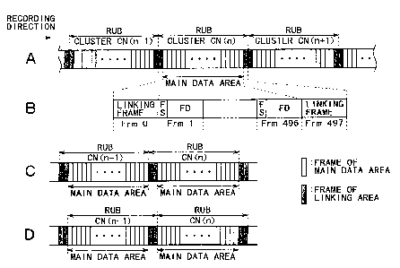
FIGS. 1A, 1B, 1C, and 1D show structures of RUBS as
units (recording and reproducing units) of reproducing
channel data.
As shown in FIG. 1A, RUBS are recorded in order as
a continuous sequence from a data recording start
position on the disk at predetermined positions specified
by addresses on the disk.
In this case, RUBS at cluster addresses CN(n - 1),
CN(n), and CN(n + 1) are shown.
A cluster is a unit of 64 KB; and corresponds to a
main data area of the RUB. A unit obtained by adding a
linking area to the cluster of 64 KB is referred to
herein as the RUB.
Therefore a cluster address can also be said to be
an address of an RUB unit.
16
CA 02452982 2003-12-11
As shown in FIG. 1B, an RUB comprises 498 frames
FrmO to Frm497.
In FIG. 1A, each RUB is shown divided into frame
units. Hatched frames form linking areas, whereas
unhatched frames form main data areas.
As shown in FIGS. 1A and 1B, in the case of the
rewritable disk, a start frame FrmO and an end frame
Frm497 of each RUB are frames as a linking area, and
frames Frm1 to Frm496 are frames as a main data area.
Each of 496 frames (Frml to Frm496 in the case of
FIGS. 1A and 1B) forming a main data area has a frame
sync FS disposed at a start of the frame, and has frame
data FD disposed so as to succeed the frame sync FS. The
frame sync FS is 30 channel bits. Main data (user data)
is recorded as the frame data FD.
Each frame is 1932 channel bits including the frame
sync FS of 30 channel bits.
Incidentally, a frame (FrmO or Frm497 in the case
of FIGS. 1A and 1,B) forming a linking area is also 1932
channel bits. A structure within the frame will be
described later.
Three examples of the RUB structure of the ROM disk
according to the present embodiment, that is, a first, a
second, and a third ROM format example will be described
17
CA 02452982 2003-12-11
later. The first ROM format example is shown in FIGS. 1A
and 1B.
Specifically, in the example, :Frames forming a
linking area are added with one frame on each of a front
end side and a rear end side of a main data area.
As shown in FIG. 1C, in the second ROM format
example, first two frames of an RUB form a linking area.
That is, in this case, frames FrmO and Frml form a
linking area, and frames Frm2 to Frm497 form a main data
area.
As shown in FIG. 1D, in the third ROM format
example, two frames at an end of an RUB form a linking
area. That is, in this case, frames Frm496 and Frm497
form a linking area, and frames FrmO to Frm495 form a
main data area.
Incidentally, in the following description, frames
forming a linking area will also be referred to as
"linking frames," and frames forming a main data area
will also be referred to as "data frames."
2. Scrambling System
A scrambling system used in the present embodiment
will next be described.
Scrambling processing to be described below is
18
CA 02452982 2003-12-11
performed on not only frame data FD (main data: user
data) recorded in frames as a main data area as described
above but also data in frames as a linking area on the
ROM disk according to the present embodiment.
FIG. 2 schematically shows a scrambling circuit.
Thirty-two bits PS0 to PS31 represent a physical sector
number.
The physical sector number is a physical address
for a sector of 2-KB data, and is 4 bytes (32 bits). When
recording and reproduction is performed in units of one
cluster of 64 KB forming one RUB, 32 physical sector
numbers are assigned to one cluster.
Fifteen bits PS5 to PS19 of the 32-bit physical
sector number represent a cluster number (a cluster
address CN of an RUB unit).
The scrambling circuit comprises a 16-bit shift
register 1 based on a polynomial ~ (x) - X16 + X15 + X13 +
X4 + 1, and exclusive-bR circuits (EX-OR circuits) 2, 3,
and 4. _
SO to S15 denotes data retained in the shift
register 1.
The shift register 1 shifts a value of data Sn to
S(n + 1) for each clock of a shift c7_ock CKs (n = 0 to
14) .
19
CA 02452982 2003-12-11
However, a value obtained via the EX-OR circuits 2,
3, and 4 is inputted as data S0. That is, supposing that
"$" denotes exclusive-or logic, (S15) $ (S14) $ (S12)
$ (S3) is inputted as data S0.
In the scrambling method, at a start of a data
block (RUB) to be scrambled, the data SO to S15 is loaded
into the shift register 1 on the basis of a parallel load
signal PL.
In this case, the values of PS:5 to PS19 in the
physical sector number are loaded as the data SO to 514.
Incidentally, the thus preset physical sector number is a
first physical sector number in the cluster.
A fixed value "1°' is loaded as the data 515.
The cluster number in the physical sector number is
thus preset as initial values as the data SO to S15 in
the shift register 1. The first data SO to S7 at this
time becomes a first scrambling byte SCB.
Then, data SO to S7 after an 8-bit shift becomes a
next scrambling byte SCB. ,
As shown in FIGS. 1A to 1D, there are two frames
forming a linking area in one RUB.
Data in one frame excluding the frame sync is 155
bytes, and a two-frame section is 310 bytes.
Suppose that the data of 310 bytes recorded in a
CA 02452982 2003-12-11
linking area is data DO to D309. hn this case, the
scrambling circuit repeats an 8-bit shift 309 times. That
is, the data SO to 57 at the time of loading and data SO
to S7 at the time of each of the 309 8-bit shifts after
the loading form scrambling bytes (SCBO to SCB309) for
the data DO to D309.
Then, the data DO to D309 in the linking area is
scrambled by the scrambling bytes (SCBO to SCB309).
Specifically, supposing that original data (data
before being scrambled) of the data DO to D309 recorded
in the linking area is LDO to LD309, the data DO to D309
is scrambled as
D(k) - (LD(k) ) $ (SCB(k) )
where $ denotes exclusive-or logic, and "k" is a value of
0 to 309.
r
In practice, supposing that the original data LDO
to LD309 to be recorded in the linking area is all zero
data, the 320 scrambling bytes (SCBO to SCB309) obtained
as described above are set as..they are as the data DO to
D309 in the linking area by the above-described
scrambling processing.
When the original data LDO to LD309 to be recorded
in the linking area is significant data, for example data
used for control or management, the data LDO to LD309 is
21
CA 02452982 2003-12-11
scrambled by the respective scrambling bytes (SCBO to
SCB309) to become the data DO to D309 of the linking area.
Incidentally, while in this case, the scrambling
bytes SCBO to SCB309 are obtained by the 309 8-bit shifts
after initial value presetting, presetting may be
performed for frame units (units of 1.55 bytes) (154 8-bit
shifts) to obtain scrambling bytes (SCBO to SCB154) in
correspondence with data of each of the two linking
frames .
In this case, "k" in the above expression D(k) -
(LD(k) ) $ (SCB(k) ) is a 'value of 0 to 154.
Supposing that the original data LDO to LD309 to be
recorded in the linking area is all zero data, each of
the data DO to D154 and the data D155 to D309 is, in the
result, values of the scrambling bytes (SCBO to SCB154).
On the other hand, the scrambling circuit repeats
the 8-bit shift 2051 times for a 2-KB unit in a main data
area of a cluster of 64 KB. A scrambling byte (SCBO to
SCB2051) as data SO to S7 is obtained as a result of each
8-bit shift.
Incidentally, there are 32 2-KB sectors to which a
physical sector number is assigned within one cluster.
Since the initial value loaded into the shift register 1
is the same cluster number, the scrambling bytes {SCBO to
22
CA 02452982 2003-12-11
SCB2051) are the same for the 32 sector,units of 2 KB
each.
Suppose that main data, that is, scrambled data
recorded in each 2-KB sector in a cluster is RDO to
RD2051.
Then supposing that original data before being
scrambled is UDO to UD2051, the data is scrambled as
RD(k) - (UD(k) ) $ (SCB(k) )
where $ denotes exclusive-or logic, and "k" is a value of
0 to 2051:
A synchronizing signal (frame sync FS) is added to
a frame unit of the thus scrambled data RDO to RD2051,
and then the data RD0 to RD2051 is recorded on the disk.
3. Data Format of Rewritable Disk
The ROM disk according to the present embodiment
has as one object a data format suitable for
compatibility with the rewritable disk. Therefore, prior
to description of the ROM disk according to the present
embodiment, a data format of the rewritable disk will be
described.
FIGS. 3A and 3B show details of a portion including
a boundary portion between an RUB and a next RUB, that is;
a linking area.
23
CA 02452982 2003-12-11
The portion shown in the figures includes RUBS
having cluster numbers CN(n - 1), CN(n), and CN(n + 1),
respectively, as PS5 to PS19 of the above-described
physical sector number.
As shown in FIG. 1A, one RUB has a start frame FrmO
and an end frame Frm497 as linking area frames. Thus, a
linking area of two frames is formed between a main data
area of an RUB and a main data area of a next RUB.
The linking area of two frames can be made to have
various functions as an RUB buffer.
For example, the linking area is used for PLL clock
pull-in in data recording and reproduction. Also, the
lirLking area can be used for automatic adjustment of
laser power (APC: Automatic Power Corztral) in data
recording.
The linking area can also serve as a buffer area to
deal with recording position variatians due to recording
start position accuracy.
The linking area can also be a.,buffer for enabling
processing referred to as a start position shift. The
start position shift refers to a position shift when a
start position of each recording unit block is shifted
from a specified start position by random channel bits to
avoid excessive wear of the disk.
24
CA 02452982 2003-12-11
Further, the linking area can be used as a temporal
buffer area for time-requiring processing such as
waveform equalizing processing and Vi.terbi decoding
processing at a time of reproduction, for example.
Further, the linking area can be used for laser
power APC at a time of ending recording of a block:
As shown in FIG. 3B, a frame FrmO as a linking
frame at a start of an RUB has a sync; S2 recorded at a
position 20 channel bits before a frame sync FSO of a
data frame Frml at a start of a cluster, and has a sync
S1 recorded at a position 40 channel bits before the sync
S2. The sync S1 and the sync S2 are synchronizing signals
for indicating a start (= frame Frml) of data frames.
In a portion other than the sync S1 and the sync S2
in the linking frame FrmO, a pattern of 3T, 3T, 2T, 2T,
5T, and 5T (T is channel bit length) is recorded
repeatedly.
A frame Frm497 as a linking frame at an end of an
RUB. has a frame sync S3 recorded at a start of the frame,
and subsequently has a 9T pattern recorded six times as
information for indicating an end of data frames. In the
other portion, a pattern of 3T, 3T, 2T, 2T, 5T, and 5T is
recorded repeatedly.
Data frames forming a main data area are frames
CA 02452982 2003-12-11
Frml to Frm496.
A frame sync FS is recorded at a head of each data
frame. Though frame sync patterns will be described later,
a frame sync of a sync pattern FSO is recorded in the
data frame Frml, and a frame sync of a sync pattern FS2
is recorded in the data frame Frm496, as shown in FIG. 3B:
The main data area of the frames Frm1 to Frm496 has
32 2-KB sectors recorded therein, the 32 2-KB sectors
being scrambled by the above-described scrambling circuit
by scrambling bytes SCBO to SCB2051 obtained when the
cluster number is set as a preset value (shift register
initial value).
Each of the frames FrmO to Frm497 forming the RUB
is formed by 1932 channel bits including 30 channel bits
of the frame sync FS after modulation.
The scramble as described above is performed to
prevent a worst pattern difficult to detect from
continuing in modulated patterns on the rewritable disk.
4. First Example of Data Format of ROM Disk
FIGS. 4A and 4B show a first example of a ROM
format.
As in FIGS. 3A and 3B, a portion shown in FIGS. 4A
and 4B includes RUBs having cluster numbers CN(n - 1),
26
CA 02452982 2003-12-11
CN(n), and CN(n + 1) (PS5 to PS19 of physical sector
numbers), respectively.
As is also shown in FIG. 1A, in the first format
example, one RUB has a start frame FrmO and an end frame
Frm497 as linking frames. Frames Frml to Frm496 are data
frames forming a main data area.
Thus, the linking area of the two frames is formed
between a main data area of an RUB and a main data area
of a next RUB.
As shown in FIG. 4B, the frame FrmO as the linking
frame at a start of the RUB has a sync S4 recorded at a
head position of the frame. The frame Frm497 as the
linking frame at-an end of the RUB has a sync S3 recorded
at a head position of the frame.
In addition to the sync S4 and. the sync S3, linking
data DO to D309 is recorded in the linking frames FrmO
and Frm497.
In this case, the linking data DO to D154 is
recorded in the linking. frame FrmO, and the linking data
D155 to D309 is recorded in the linking frame Frm497.
As described in the scrambling system, the linking dat a
DO to D309 is scrambled by the scrambling circuit in FIG.
2 by scrambling bytes SCBO to SCB309 obtained when the
cluster number is set as a preset value (shift register
27
CA 02452982 2003-12-11
initial value).
Supposing that original data to be converted into
the linking data is all zero data, the scrambling bytes
SCBO to SCB154 are recorded as they are as the data DO to
D154 in the linking frame FrmO, and the scrambling bytes
SCB155 to SCB309 are recorded as the data D155 to D309 in
the linking frame Frm497.
Incidentally, when the preset value is updated for
frame units in the scrambling processing as described
above, the linking data DO to D154 and the linking data
D155 to D309 are each scrambled by the scrambling bytes
SCBO to SCB154.
Data frames forming a main data area are frames
Frml to Frm496.
A frame sync FS is recorded at a head of each data
frame. As shown in FIG. 4B, a frame sync of a sync
pattern FSO is recorded in the data frame Frml, and a
frame sync of a sync pattern FS2 is recorded in the data
frame Frm496.
The main data area of the frames Frml to Frm496 has
32 2-KB sectors recorded therein, the 32 2-KB sectors
being scrambled by the scrambling circuit in FIG. 2 by
scrambling bytes SCBO to SCB2051 obt<~ined when the
cluster number is set as a preset value (shift register
28
CA 02452982 2003-12-11
a
initial value).
Each of the frames FrmO to Frm497 forming the RUB
is formed by 1932 channel bits including 30 channel bits
of the frame sync FS after modulation..
Such a ROM format having linking areas is
advantageous in terms of compatibility with the
rewritable disk.~Specifically, the ROM format is
advantageous for designing a reproducing apparatus
supporting both the rewritable disk and the ROM disk, and
is suitable for simplifying the apparatus and reducing
cost of the apparatus.
In addition, frames within RUBS including linking
areas are scrambled by scrambling bytes generated by a
random sequence with each physical sectar number (cluster
number) as an initial value. Therefore the scrambled
frames do not form the same data stream as in an adjacent
track, so that a highly accurate DPD signal can be
obtained. The ROM format is thus suitable for a tracking
servo using the..DPD signal.
Further, linking frames and data frames within an
RUB are scrambled by scrambling data generated by the
same system, that is, scrambling bytes SCB generated
using the cluster number as an initial value, as
described with reference to FIG. 2. This eliminates the
29
CA 02452982 2003-12-11
need for providing separate scrambling processing
circuits or separate descrambling processing circuits for
linking areas and main data areas, anal thus makes it
possible to simplify circuit configuration.
Further, because of the sync S3 and the sync S4, a
sync pattern occurs regularly in each frame section
regardless of whether the frame section includes a
linking area. The ROM format is therefore advantageous
for frame synchronization protection and frame
synchronization pull-in.
In the case of the ROM disk, in particular, since
there is no wobbling groove on the RGM disk, spindle
rotational speed information is obtained on the basis of
sync detection. This can be performed properly because a
sync pattern occurs regularly in each frame section. That
is, the ROM format is advantageous for generating a
spindle PLL phase error signal using the sync pattern.
Even in a PLL non-synchronization state, in particular,
intervals at which the sync pattern occurs can be used as
rotational speed information.
5. Second Example of Data Format of ROM Disk
FIGS. 5A and 5B show a second example of a ROM
format.
CA 02452982 2003-12-11
As in FIGS. 4A and 4B, a portion shown in FIGS. 5A
and 5B includes RUBs having cluster numbers CN(n - 1),
CN(n), and CN(n + 1) (PS5 to PS19 of physical sector
numbers); respectively.
As is also shown in FIG. 1.C, in the second format
example, first two frames FrmO and Frml of one RUB are
linking frames. Frames Frm2 to Frm497 are data frames
forming a main data area.
Thus, the linking area of the two frames is formed
between a main data area of an RUB and a main data area
of a next RUB.
As shown in FIG. 5B, the frame FrmO as the linking
frame at a start of the RUB has a sync S3 recorded at a
head position of the frame. The next linking frame Frm1
has a sync S4 recorded at a head position of the frame.
In addition to the sync S3 and the sync S4, linking
data DO to D309 is recorded in the linking frames FrmO
and Frml.
In this case, the linking data DO to D154 is
recorded in the linking frame FrmO, and the linking data
D155 to D309 is recorded in the linking frame Frml.
As. described in the scrambling system, the linking
data DO to D309 is scrambled by the scrambling circuit in
FIG. 2 by scrambling bytes SCBO to SCB309 obtained when
31
CA 02452982 2003-12-11
the cluster number is set as a preset. value (shift
register initial value).
Supposing that original data to be converted into
the linking data is all zero data, the scrambling bytes
SCBO to SCB154 are recorded as they are as the data DO to
D154 in the linking frame FrmO, and the scrambling bytes
SCB155 to SCB309 are recorded as the data D155 to D309 in
the linking frame Frml.
Incidentally, when the preset value is updated for
frame units in the scrambling processing as described
above, the linking data DO to D154 and the linking data
D155 to D309 are each scrambled by the scrambling bytes
SCBO to SCB154.
Data frames forming a main data area are frames
Frm2 to Frm497.
A frame sync FS is recorded at a head of each data
frame. As shown in FIG. 5B, a frame sync of a sync
pattern FS0 is recorded in the data frame Frm2, and a
frame sync of a sync pattern FS2 is recorded in the data
frame Frm497.
The main data area of the frames Frm2 to Frm497 has
32 2-KB sectors recorded therein, the 32 2-KB sectors
being scrambled by the scrambling circuit in FIG. 2 by
scrambling bytes SCBO to SCB2051 obtained when the
32
CA 02452982 2003-12-11
cluster number is set as a preset value (shift register
initial value).
Each of the frames FrmO to Frm497 forming the RUB
is formed by 1932 channel bits including 30 channel bits
of the frame sync FS after modulation.
The second ROM format example can provide the same
effects as the first ROM format example described above.
6. Third Example of Data Format of ROM Disk
FIGS. 6A and 6B show a third example of a ROM
format.
As in FIGS. 5A and 5B, a portion shown in FIGS. 6A
and 6B includes RUBS having cluster numbers CN(n - 1),
CN(n), and CN(n + 1) (PS5 to PS19 of physical sector
numbers), respectively.
As is also shown in FIG. 1D, in the third format
example, two end frames Frm496 and Frm497 of one RUB are
linking frames. Frames FrmO to Frm495 are data frames
_, forming a main data area. .,
Thus, the linking area of the two frames is formed
between a main data area of an RUB and a main data area
of a next RUB.
As shown in FIG. 6B, the second last frame Frm496
as the linking frame in the RUB has a sync S3 recorded at
33
CA 02452982 2003-12-11
a head position of the frame. The next linking frame
Frm497 has a sync S4 recorded at a head position of the
f r ame .
In addition to the sync S3 and the sync S4, linking
data DO to D309 is recorded in the linking frames Frm496
and Frm497.
In this case, the linking data DO to D154 is
recorded in the linking frame Frm496, and the linking
data D155 to D309 is recorded in the linking frame Frm497.
As described in the scrambling system, the linking
data DO to D309 is scrambled by the scrambling circuit in
FIG. 2 by scrambling bytes SCBO to SCB309 obtained when
the cluster number-is set as a preset value (shift
register initial value).
Supposing that original data to be converted into
the linking data is all zero data, the scrambling bytes
SCBO to SCB154 are recorded as they a.re as the data DO to
D154 in the linking frame Frm496, and the scrambling
,, bytes SCB155 to SCB309 are recorded a.s the data D155 to
D309 in the linking frame Frm497.
Incidentally, when the preset 'value is updated for
frame units in the scrambling processing as described
above, the linking data DO to D154 anal the linking data
D155 to D309 are each scrambled by the scrambling bytes
34
CA 02452982 2003-12-11
SCBO to SCB154.
Data frames forming a main data area are frames
FrmO to Frm495.
A frame sync FS is recorded at a head of each data
frame. As shown in FLG. 6B, a frame .sync of a sync
pattern FSO is recorded in the data frame FrmO, and a
frame sync of a sync pattern FS2 is recorded in the data
frame Frm495.
The main data area of the frames FrmO to Frm495 has
32 2-KB sectors recorded therein, the 32 2-KB sectors
being scrambled by the scrambling circuit in FIG. 2 by
scrambling bytes SCBO to SCB2051 obtained when the
cluster number is set as a preset value (shift register
initial value).
Each of the frames FrmO to Frm497 forming the RUB
is formed by 1932 channel bits including 30 channel bits
of the frame sync FS after modulation.
The third RO~ format example can provide the same
_, effects as the first ROM format example described above.
7. ECC Block and Address
As described above, the present example uses an
address value of a physical sector nL~mber (cluster
number) as an initial value for obtaining a scrambling
CA 02452982 2003-12-11
byte. Accordingly, a structure of an ECC block and
addresses will be described in the following.
FIGS. 7A, 7B, 7C, and 7D show an ECC format for
main data (user data).
As ECC (error correction code), there are two codes,
that is, LDC (long distance code) for main data of 64 KB
(= 2048 bytes per sector X 32 sectors) forming one
cluster and BIS (burst indicator subcode).
The main data of 64 KB shown i:n FIG. 7A is ECC-
encoded as shown in FIG. 7B. That is, an EDC (error
detection code) of 4 B is added to on.e sector of 2048 B
of the main data, and LDC is encoded for the 32 sectors.
The LDC is an RS (reed solomon) (248, 216, 33) code with
a code length of 248 symbols, data of 216 symbols, and a
distance of 33 symbols. There are 304 code words.
On the other hand, BIS is ECC-encoded as shown in
FIG. 7D for data of 720 B shown in FIG. 7C. Specifically,
the BIS is an RS (reed Solomon) (62, 30, 33) code with a
code length of 52 symbols, data of 3C1__symbols, and a
distance of 33 symbols. There are 24 code words.
FIG. 8 shows a frame structure of the main data.
The LDC data and the BIS form the frame structure
shown in the figure. Specifically, data (38 B), BIS (1 B),
data (38 B), BIS (1 B), data (38 B), BIS (1 B), and data
36
CA 02452982 2003-12-11
(38 B) are arranged per frame to form a structure of 155
B. That is, one frame is formed by data of 38 B X 4, or
152 B, and BIS of 1 B inserted between each 38 B.
A frame sync FS (frame synchronizing signal) is
disposed at the head of one frame of 155 B. One block has
496 frames.
The LDC data has a 0th, a 2nd, ... even-numbered
code word placed in a 0th, a 2nd, ... even-numbered frame
and a 1St, a 3rd, ....odd-numbered code word placed in a
1St, a 3rd, .. odd-numbered frame.
BIS uses a code much superior to the code of LDC in
correction capability. Almost all errors are corrected.
That is, a code with a distance of 33 symbols for a code
length of 62 symbols is used.
Thus, BIS symbols when errors are detected can be
used as follows.
In ECC decoding, BIS is decoded first. When two
adjacent to each other of BISs and a frame sync FS in the
frame structure of FIG. 8 have an error,.data of 38 B
sandwiched between the two is considered to have a burst
error. An error painter is added to the data of 38 B: In
LDC, this error pointer is used to make pointer erasure
correction.
Thereby correction capability can be enhanced as
37
CA 02452982 2003-12-11
compared with correction using only LDC.
BIS includes address information and the like. The
address is used when there is rio address information in
the form of a wobbling groove, as is the case with the
ROM disk in this example or the like.
In the main data block structure of FIG. 8, address
units are formed as shown in FIG. 9.
Specifically, in the main data block, 16 address
unit s "0" to "15" are formed. One address unit comprises
31 frames.
Address fields including a physical sector number
as address information and error correcting information
are recorded in BISs in each address unit.
The address fields are formed by 9 bytes. As shown
in FIG. 9, each frame has a BIS of 1 byte at three
positions. BISs in three consecutive frames at a head of
each address unit, that is, BISs of 9 bytes are address
fields 0 to 8. In FIG. 9, address fields of each address
unit ar,e indicated simply by numerals 0 to 8.
A cluster number in a first physical sector number
in the main data block of 64 KB, that is, the cluster is
used as an initial value in the scrambling circuit of FIG.
2. Thus, in reproduction, descrambling processing is
performed using the cluster number in the physical sector
38
CA 02452982 2003-12-11
number to reproduce the main data.
FIG. 10 shows address units and address fields of
physical sector numbers included in BISs as described
above.
In the main data block of 64 KB, 16 physical sector
numbers are set by the 16 address units "0" to "15."
Each address unit comprises 9 bytes of address
fields (AFO, S) to (AF8, S) (where S is 0 to 15).
The 4 bytes of address fields (AFO, S) to (AF3, S)
represent a 4-byte physical sector number as described
above. (AFO, S) is on an MSB side, and (AF3, S) is on an
LSB side.
The address field (AF4, S) is flag bits.
The address fields (AF5, S) to (AF3, S) are RS (9,
5, 5) parity. The address fields (AFO, S) to (AF4, S) are
RS (9, 5, 5) data.
8. Sync Patterns and Order
As,described in each ROM disk format example, a
frame sync FS is recorded at a head of each of 496 data
frames. A sync S3 and a sync S4 are recorded in linking
f r ame s .
For addressing within the main data block, the 496
frames of the RUB are divided into 16 address units
39
CA 02452982 2003-12-11
(physical sectors) of 31 frames each, as described above.
By detecting a pattern of a frame sync FS, a frame
number (0 to 30) of each of 31 frames within a physical
sector can be detected. Thus, address>es of frame units
can be detected. That is, an address of a frame unit
within data can be obtained as an RUB/sector number and
frame number.
As shown in FIG. 11A, seven sync patterns FSO to
FS7 are defined as sync patterns used as frame syncs FS
and syncs S3 and S4.
Each of the sync patterns FSO to FS7 comprises a
main body (sync body) of,a 24-bit pattern out of rules of
RLL {1, 7) PP modulation and a sync ID of 6 bits as
identifying information.
The sync patterns are defined by modulation bits.
"1" shown in the bit examples of FIG. 11A denotes signal
inversion. Before recording onto a disk, such a frame
sync code is converted into an NRZI channel bit stream.
That is, the"sync body is "01010000000010000000010," a
pattern in which 9T inverted at "1" is repeated twice
continuously, as shown in FIG. 11A.
Zero or one is inserted in # at a head of the sync
body so that a pattern preceding # satisfies the rules of
RLL (1, 7) PP modulation.
CA 02452982 2003-12-11
The sync patterns FSO to FS7, having the same sync
body, are distinguished from each other by sync ID.
A physical sector as a unit of 31 frames in a main
data block of an RUB has sync patterns FSO to FS6 mapped
as shown in FIG. 11B so that the 31 frames can be
identified by frame sync FS.
Since seven kinds of sync patterns are not
sufficient to identify the 31 frames, the seven kinds of
frame syncs FS (FSO to FS6) are arranged in predetermined
order, so that a frame is identified by a combination of
a preceding frame sync and a succeeding frame sync.
As shown in FIG. 11B, a first frame (frame number
0) of each physical sector has a sync pattern FSO. The
sync pattern FSO is unique within the physical sector,
thereby making it easy to detect a head of the physical
sector, that is, the address unit. That is, the sync
pattern FSO is used to detect the position of a physical
sector number.
The other,frames (frame numbers 1 to 30) are
assigned sync patterns FS1 to FS6 as shown in FIG. 11B.
In this case, a sequence of sync patterns of any
five consecutive frame syncs is unique. When two of five
consecutive frame syncs are detected, it is possible to
detect the position of the frames within the address unit.
41
CA 02452982 2003-12-11
Specifically, a frame number n can be identified
from a combination of a sync pattern of the frame number
n and a sync pattern of one of frame numbers n - 1, n - 2,
n - 3, and n - 4.
For example, supposing that a frame number of a
present frame is 5 (fifth frame), even when frame syncs
FS (FS1, FS2, and FS3) of a first, a second, and a third
frame preceding the fifth frame are lost, the present
frame can be identified as having the frame number 5 from
a frame sync FS (FS3) of a fourth frame immediately
preceding the fifth frame and a frame sync FS (FSI) of
the present frame (fifth frame). This is because the sync
pattern FSl comes next to the sync pattern FS3 only in a
specific position in FIG. 11B, that is, the frame numbers
4 and 5.
As shown in the first, second, and third ROM format
examples in FIGS. 4A and 4B, FIGS. 5A and 5B, and FIGS.
6A and 6B, syncs S3 and S4 are recorded in linking frames.
The sync pattern FS7 is used for the sync S3, and the
sync pattern FS2 is used for the sync S4.
Incidentally, for the syncs S1, S2, and S3 shown in
FIGS. 3A and 3B in the case of the rewritable disk, the
sync patterns FS4, FS6, and FSO are used, respectively.
In the first, second, and third ROM format examples
42
CA 02452982 2003-12-11
in FIGS. 4A and 4B, FIGS. 5A and 5B, and FIGS. 6A and 6B,
all sequences of five consecutive frame syncs are not
unique when the linking area is included. However, by
using the sync patterns FS7 and FS2 as the syncs S3 and
S4, respectively, a sequence of any four consecutive
frame syncs is unique. When two of four consecutive frame
syncs are detected, it is possible to detect the position
of the frames within the linking area and the address
unit.
9. Disk Drive Apparatus
A disk drive apparatus capable of performing
recording/reproduction of a disk 1 as a ROM disk or a
rewritable disk as described above will next be described.
FIG. 12 shows a configuration of the disk drive
apparatus.
The disk 1 is loaded onto a turntable not shown in
the figure, and is driven by a spindle motor 52 to be
rotated at a constant linear velocity (CLV) at the time
of recording/reproducing operation.
Then an optical pickup (optical head) 51 reads data
on the disk l, that is, data in the form of embossed pits
in the case of the ROM disk or data in the form of phase
change marks in the case of the rewri.table disk.
43
CA 02452982 2003-12-11
In the case of the rewritable disk, t:he optical pickup 51
reads ADIP information and disk information embedded as
wobbling of a groove track.
At the time of recording on the rewritable disk,
the optical pickup records data as phase change marks on
the groove track.
Formed within the optical pickup 5l are: a laser
diode serving as a laser light source; a photodetector
for detecting reflected light; an objective lens at an
output end of laser light; and an optical system (not
shown) for irradiating a recording surface of the disk
with the laser light via the objective lens and guiding
the reflected light to the photodetector.
The laser diode outputs a so-called blue laser with
a wavelength of 405 nm. An NA of the optical system is
0.85.
The objective lens within the pickup 51 is held by
a two-axis mechanism so as to be movable in a tracking
., direction and a focus direction.
The pickup 51 as a whole is movable in a direction
of the radius of the disk by a sled mechanism 53.
The laser diode in the pickup 51 is driven by a
drive signal (drive current) from a laser driver 63 to
emit laser light.
44
CA 02452982 2003-12-11
The photodetector detects information as the light
reflected from the disk l, converts the information into
an electric signal corresponding to the amount of light
received, and then supplies the electric signal to a
matrix circuit 54.
The matrix circuit 54 has a current-voltage
conversion circuit, a matrix calculation/amplification
circuit and the like for output currents from a plurality
of light receiving elements as the photodetector. The
matrix circuit 54 generates necessary signals by matrix
calculation processing.
For example, the matrix circuit 54 generates a
high-frequency signal (reproduced data signal)
corresponding to reproduced data; a focus error signal
and a tracking error signal for servo control, and the
like.
The matrix circuit 54 generates a push-pull signal,
for example, as the tracking error signal in the case
where the disk 1 is a rewritable disk, whereas the matrix
circuit 54 generates a DPD signal, for example, as the
tracking error signal in the case where the disk 1 is a
ROM disk.
Further, the matrix circuit 54 generates a push-
pull signal as a signal related to groove wobbling, that
CA 02452982 2003-12-11
is, a signal for detecting wobbling.
Incidentally, the matrix circuit 54 may be formed
within the pickup 51.
The reproduced data signal outputted from the
matrix circuit 54 is supplied to a reader/writer circuit
55; the focus error signal and the tracking error signal
are supplied to a servo circuit 61: and the push-pull
signal as wobbling groove detecting information is
supplied to a wobble circuit 58.
The reader/writer circuit 55 subjects the
reproduced data signal to binarization processing,
reproduced clock generation processing by a PZL and the
like, thereby reproduces data read from phase change
marks or embossed pits, and then supplies the data to a
modulating and demodulating circuit 56.
The modulating and demodulating circuit 56 has a
functional part as a decoder at the time of reproduction
and a functional part as an encoder at the time of
. recording. ~,
As decode processing at the time of reproduction,
the modulating and demodulating circuit 56 demodulates a
run length limited code on the basis of a reproduced
clock.
An ECC/scramble circuit 57 performs ECC encode
46
CA 02452982 2003-12-11
processing that adds error correction codes and the
scramble processing as described with. reference to FIG. 2
at the time of recording.
The ECC/scramble circuit 57 performs descrambling
processing for the scrambling processing as described
with reference to FIG. 2, and performs ECC decode
processing for error correction at trre time of
reproduction.
At the time of reproduction, the ECC/scramble
circuit 57 captures the data demodulated by the
modulating and demodulating circuit 56 into an internal
memory, then performs the descrarnbling processing and
error detection/correction processing, and thereby
obtains reproduced data.
In the descrambling processing, as described with
reference to FIG. 2, the ECC/scramble circuit 57
generates scrambling bytes for data of linking frames and
data frames of each RUB on the basis of a cluster number
of a physical sector address obtained by an address
decoder 59. Using the scrambling bytes, the ECC/scramble
circuit 57 performs the descrambling processing for the
above-described scramble processing.
The ECC encode processing and the ECC decode
processing of the ECC/scramble circuit 57 correspond to
47
CA 02452982 2003-12-11
the ECC format using the RS (reed solomon) (248, 216, 33)
code with a code length of 248 symbols, data of 216
symbols, and a distance of 33 symbols.
The data decoded to the reproduced data by the
ECC/scramble circuit 57 is read and transferred to an AV
(Audio-Visual) system 120 on the basis of an instruction
from a system controller 60.
In the case where the disk 1 is the rewritable disk,
the push-pull signal outputted from the matrix circuit 54
as the signal related to groove wobbling is processed in
the wobble circuit 58. The push-pull signal as ADIP
information is subjected to MSK demodulation and HMW
demodulation in the wobble circuit 58, thereby
demodulated into a data stream constituting an ADIP
address, and then supplied to the address decoder 59.
The address decoder 59 decodes the data supplied
thereto, thereby obtains an address value, and then
supplies the address value to the system controller 60.
Also, the address decoder 59 generates a clock by
PLL processing using a wobble signal supplied from the
wobble circuit 58, and supplies the clock to various
parts as an encode clock at the time of recording, for
example.
In the case where the disk 1 is the ROM disk, the
48
CA 02452982 2003-12-11
0
address decoder 59 performs frame sync synchronization
processing on the basis of the reproduced data signal,
and reads address information, that is, a physical sector
number by obtaining information of address fields
included in the BISs described above. The address
information obtained is supplied to the system controller
60. In this case, the clock reproduced by the PLL in the
reader/writer circuit 55 is used as a. clock for address
detection.
At the time of recording on the rewritable disk,
recording data is transferred from the AV system 120: The
recording data is supplied to the memory in the
ECC/scramble circuit 57 to be buffered.
In this case, as processing for encoding the
buffered recording data, the ECC/scramble circuit 57
performs addition of error correction codes, scramble
processing, and addition of subcodes and the like.
The ECC-encoded and scrambled data is subjected to
RLL.,(1-7) PP modulation in the modulating, and
demodulating circuit 56, and then supplied to the
reader/writer circuit 55.
As described above, the clock generated from the
wobble signal is used as the encode clock serving as a
reference clock for the above encode processing at the
49
CA 02452982 2003-12-11
time of recording.
The recording data generated by the encode
processing is supplied as a laser drive pulse to the
laser driver 63 after as recording compensation
processing, the reader/writer circuit 55 adjusts the
waveform of the laser drive pulse and finely adjusts
optimum recording power, for example, to characteristics
of a recording layer, spot shape of the laser light,
recording linear velocity and the like.
The laser driver 63 provides the laser drive pulse
supplied thereto to the laser diode within the pickup 5I
and thereby drives the laser diode to emit laser light.
Thereby pits (phase change marks) corresponding to the
recording data are formed on the disk 1.
The laser driver 63 has a so-called APC (Automatic
Power Control) circuit to control laser output at a
constant level without depending on the temperature and
the like while monitoring laser output power through
output of a laser power monitoring detector provided
within the pickup 51. Target values of the laser output
at the time of recording and at the time of reproduction
are supplied from the system controller 60, and the laser
output level is controlled to be at the target values at
the time of recording and at the time of reproduction,
CA 02452982 2003-12-11
a
0
respectively.
The servo circuit 61 generates various servo drive
signals for focus, tracking, and the sled from the focus
error signal and the tracking error signal supplied from
the matrix circuit 54, to thereby perform servo operation.
Specifically, the servo circuit 61 generates a
focus drive signal and a tracking drive signal according
to the focus error signal and the tracking error signal,
to drive a focus coil and a tracking coil of the two-axis
mechanism within the pickup 51. Thereby a tracking servo
loop and a focus servo loop are formed by the pickup 51,
the matrix circuit 54, the servo circuit 61, and the two-
axis mechanism.
In response to a track jump instruction from the
system controller 60, the servo circuit 61 turns off the
tracking servo loop and outputs a jump drive signal to
thereby perform track jump operation.
The servo circuit 6l further generates a sled drive
signal on the basis of a sled error signal obtained as a
low-frequency component of the tracking error signal,
accessing control from the system controller 60 and the
like, to drive the sled mechanism 53. Though not shown,
the sled mechanism 53 has a mechanism formed by a main
shaft for holding the pickup 51, a sled motor,
51
CA 02452982 2003-12-11
transmission gear and the like. By driving the sled motor
according to the sled drive signal, a required sliding
movement of the pickup 51 is effected.
A spindle servo circuit 62 effects control for CLV
rotation of a spindle motor 52.
The spindle servo circuit 62 obtains the clock
generated by PLL~processing on the wobble signal as
information on current rotational speed of the spindle
motor 52, and compares the information with predetermined
CLV reference speed information to thereby generate a
spindle error signal.
At the time of data reproduction, the reproduced
clock (clock as a reference for decode processingy
generated by the PLL within the reader/writer circuit 55
serves as the information on the current rotational speed
of the spindle motor 52. Hence, the spindle servo circuit
62 can also generate the spindle error signal by
comparing this information with the predetermined CLV
reference speed information.
The spindle servo circuit 62 then outputs a spindle
drive signal generated according to the spindle error
signal to thereby perform the CLV rotation of the spindle
motor 52.
Further, the spindle servo circuit 62 generates a
52
CA 02452982 2003-12-11
spindle drive signal in response to a spindle kick/brake
control signal from the system controller 60 to thereby
perform operations such as starting, stopping,
accelerating, and decelerating the spindle motor 52.
The various operations of the servo system and the
recording and reproducing system as described above are
controlled by the system controller 60 formed by a
microcomputer.
The system controller 60 performs various
processing in response to commands from the AV system 120.
For example, when a write command is issued from
the AV system 120, the system contro7_ler 60 first moves
the pickup 51 to an address where writing is to be
performed. Then the system controller 60 makes the
ECC/scramble circuit 57 and the modulating and
demodulating circuit 56 subject data (such as audio data
and video data of various systems such for example as
MPEG2) transferred from the AV system 120 to the encode
processing as described above. The laser drive pulse .is
then supplied from the reader/writer circuit 55 to the
laser driver 63 as described above, whereby recording is
performed.
When a read-command requesting transfer of some
data (MPEG2 video data or the like) recorded on the disk
53
CA 02452982 2003-12-11
1 is supplied from the AV system 120, for example, the
system controller 60 first effects seek operation control
aiming at an address specified. Specifically, the system
controller 60 issues a command to the servo circuit 61 to
effect access operation of the pickup 51 targeting the
address specified by a seek command.
Then, the system controller 10 effects operation
control necessary to transfer data of the specified data
section to the AV system 120. Specifically, the system
controller 60 effects reading of the data from the disk 1,
effects decoding/buffering and the like in the
reader/writer circuit 55, the modulating and demodulating
circuit 56, and the ECC/scramble circuit 57, and then
transfers the requested data.
At the times of recording and reproduction of data,
the system controller 60 controls access and recording
and reproducing operation using ADIP addresses or
addresses included in BISs detected by the address
decoder 59.
While the disk drive apparatus in the example of
FIG. 12 is connected to the AV system 120, the disk drive
apparatus according to the present invention may be
connected to for example a personal computer or the like.
Further, there can be an embodiment in which the
54
CA 02452982 2003-12-11
disk drive apparatus is not connected to another
apparatus. In such a case, an operation unit and a
display unit are provided, and the configuration of an
interface part for data input and output is different
from that of FIG. 12. That is, it suffices to perform
recording and reproduction in response to an operation by
a user and form a terminal part for inputting and
outputting various data.
Of course, various other configuration examples are
conceivable; for example,. an example as a reproduction-
only apparatus is conceivable.
10. Disk Manufacturing Method
A method of manufacturing the ROM disk according to
the present embodiment described above will next be
described.
A disk manufacturing process is roughly divided
into a so-called mastering process and a replication
process. The mastering process covers steps up to .,
completion of a metallic master (stamper) used in the
replication process. The replication process mass-
produces duplicate optical disks using the stamper.
Specifically; the mastering process performs so-
called mastering in which a photoresist is coated on a
CA 02452982 2003-12-11
polished glass substrate, and pits and grooves are formed
by exposing the photosensitive film to light of a laser
beam.
In the case of the present embodiment, a pit train
having an RUB structure as in the foregoing first, second,
and third ROM format examples is formed on the ROM disk.
Therefore mastering is performed to form the pit train in
the mastering process.
In mastering, main data and linking data are
subjected to necessary encode processing (such as ECC
encode and RLL (1, 7) PP encode) and scramble processing
as described with reference to FIG. ~. On the basis of
the thus formed data train, parts exposed to light as the
pit train are formed on the glass substrate.
Incidentally, the main data to be recorded is
prepared in a preparatory process referred to as
premastering.
After the mastering is completed, predetermined
processing such as development and the like is performed,
and then information is transferred onto a metallic
surface by electroforming, for example, to create a
stamper required when replicating the disk.
Then, the information is transferred onto a resin
substrate by an injection method, for example, using the
56
CA 02452982 2003-12-11
stamper, a reflective film is formed thereon, and
thereafter processing of machining into a required disk
shape and the like is performed, whereby a final product
is completed.
Mastering is performed in such a manufacturing
process. As shown in FIG. 13, for example, a mastering
apparatus comprises a controller 70, an ECC/scramble
processing unit 71, a sync processing unit 72, a switch
unit 73, a mastering unit 74, a linking data generating
unit 75, an address generating unit 16, and a scramble
processing unit 77.
The ECC/scramble processing unit 71 subjects the
main data prepared in the premastering process to ECC
error correction encode processing and scramble
processing as described with reference to FIG. 2.
The linking data generating unit 75 generates
original data LDO to LD309 of data DO to D309 to be
recorded in linking frames. The data LDO to LD309 is
. subjected to the scramble processing as described with
reference to FIG. 2 by the scramble processing unit 77 to
become the data DO to D309.
The address generating unit generates address
information as physical sector numbers. This address
information is supplied to the ECC/scramble processing
57
CA 02452982 2003-12-11
unit 71 and the scramble processing unit 77.
In encode processing, the ECC/scramble processing
unit 71 sets a physical sector number supplied thereto as
information of address fields included in BISs. Further,
in scramble processing, the ECC/scramble processing unit
71 uses a cluster number of a physical sector number as a
scramble initial value.
The scramble processing unit 7'7 also uses a cluster
number of a physical sector number supplied from the
address generating unit 76 as a scramble initial value.
The switch unit 73 selects output of the
ECC/scramble processing unit 71 during a period when
frame data corresponding to a main data area is outputted
from the ECC/scramble processing unit 71, and selects-
output of the scramble processing unit 77 during a period
when frame data corresponding to a linking area is
outputted from the scramble processing unit 77.
Consequently, a data stream of the above-described RUB
structure is supplied to the sync processing unit 72.
The sync processing unit 72 adds a frame sync FS of
a predetermined sync pattern as described above, or a
sync S3 or S4 to each frame.
Data output timing of the ECC/scramble processing
unit 71, the linking data generating unit 75, and the
58
CA 02452982 2003-12-11
address generating unit 76 and switching timing of the
switch unit 73 are controlled by the controller 70.
The mastering unit 74 includes: an optical unit (82,
83, and 84) for irradiating a photoresist-coated glass
substrate 101 with a laser beam to thereby perform
mastering: a substrate rotating/shifting unit 85 for
rotation driving and slide shifting of the glass
substrate 101; and a signal processing unit 81 for
converting input data to recording data and supplying the
recording data to the optical unit.
The optical unit includes: a laser light source 82
formed by an He-Cd laser, for example; a modulating unit
83 for modulating light emitted from the laser light
source 82 on the basis of the recording data; and a
mastering head unit 84 for condensing the modulated beam
from the modulating unit 83 and irradiating a photoresist
surface of the glass substrate 101 with the modulated
beam.
The modulating unit 83 includes: an acoustooptic
type optical modulator (AOM) for turning on/off the light
emitted from the laser light source 82; and an
acoustooptic type optical deflector (AOD) for deflecting
the light emitted from the laser light source 82 on the
basis of a wobble generating signal.
59
CA 02452982 2003-12-11
The substrate rotating/shifting unit 85 comprises:
a rotating motor for rotation-driving the glass substrate
101; a detecting unit (FG) for detecting rotational speed
of the rotating motor; a slide motor for sliding the
glass substrate 101 in a direction of the radius of the
glass substrate 101: and a servo controller fo.r
controlling the rotational speed of the slide motor and
the rotating motor, tracking of the mastering head unit
84 and the like.
The signal processing unit 81 subjects data
supplied from the sync processing unit 72 to for example
RLL (l, 7) PP modulation processing and further
modulation processing for obtaining a drive signal to be
supplied to the modulating unit 83 for mastering:
At the time of mastering, the substrate
rotating/shifting unit 85 in the mastering unit 74
rotation-drives the glass substrate 101 at a constant
linear velocity and slides the glass substrate 101 while
rotating the glass substrate 101 so that a spiral track
is formed at a predetermined track pitch.
At the same time, the light emitted from the laser
light source 82 is converted via the modulating unit 83
into a modulated beam on the basis of the modulating
signal from the signal processing unit 81, and then
CA 02452982 2003-12-11
applied from the mastering head unit 84 to the
photoresist surface of the glass substrate 101. As a
result, the photoresist is exposed to light on the basis
of the data and groove.
The controller 70 also controls performance of
operation at the time of such mastering by the mastering
unit 74.
As a result of such operation, light-exposed parts
corresponding to the pit train of an RUB structure as in
the above-described ROM format examples are formed on the
glass substrate 101.
Thereafter, development, electroforming and the
like are performed to create a stamper, and the-ROM disk
is produced using 'the stamper.
As described above, the produced ROM disk has
linking areas, and data of all frames in main data areas
and the linking areas is scrambled by scrambling bytes
SCB obtained by using a cluster number as an initial
value.
While the disk according to the present embodiment,
the disk drive apparatus compatible with the disk, and
the disk manufacturing method have been described above;
the present invention is not limited to these examples;
various modifications are conceivable without departing
61
CA 02452982 2003-12-11
from the spirit of the present invention.
As is understood from the above description, the
present invention has the following effects.
The reproduction-only recording medium (ROM disk)
according to the present invention ha.s blocks formed by
main data areas and linking areas, that is, has a data
format provided with linking areas as with the rewritable
disk. The reproduction-only recording medium according to
the present invention is thus suitable for compatibility
with the rewritable disk:
Main data recorded in a main data area and linking
data recorded in a linking area in each block are
scrambled by scrambling data generated by the same system.
The linking data being scrambled means that even
when linking areas are aligned with each other in tracks
adjacent to each ather, the pit patterns are not the same.
This solves the problem disadvantageous to the tracking
servo system using a DPD signal as an error signal, that
is, the problem of being unable to obtain a ,satisfactory
DPD signal because of the same pit patterns. In other
wards, it is possible to effect stable tracking control
on the reproduction-only recording medium with embossed
pits by the. tracking servo system using the DPD signal,
and in turn improve reproduction performance of the
62
CA 02452982 2003-12-11
r
reproducing apparatus.
In addition, the scramble processing prevents a
worst pattern from a viewpoint of detection from
continuing in main data, thus facilitating data detecaion.
Further, for main data areas and linking areas, the
scramble processing and descramble processing can be
performed by the same scrambling system. That is, the
reproducing apparatus can use a common hardware
configuration for performing scramble-related processing
on main data and linking data. This simplifies circuit
configuration of the apparatus.
The descrambling processing on the linking data is
indispensable at the time of reproduction especiallywwhen
some data is recorded as the linking data. In this case,
it is not necessary to have a plurality of descrambling
processing circuit systems.
Further, the scrambling data is generated by a
random sequence using address information of a block as
an initial value. This means that the initial.value
differs for different blocks. That is, the pit pattern is
scrambled and formed in a different state in each block.
Therefore cases in which the pit pattern is the same
between adjacent linking areas, including for example
cases where the linking data is all ~:ero data or
63
CA 02452982 2003-12-11
identical pattern data, do not occur. Thus a desirable
state for servo control using the DPD signal can be
realized.
Further, the disk manufacturing method according to
the present invention makes it possible to manufacture a
reproduction-only recording medium providing these
effects.
64