Note: Descriptions are shown in the official language in which they were submitted.
CA 02453107 2004-O1-06
WO 03/007319 PCT/US02/17897
CAPACITOR HAVING EPOXY DIELECTRIC LAYER CURED WITH
AMINOPHENYLFLUORENES
This invention relates to an electrical article, methods for making the
electrical
article, and circuit articles made therefrom.
The embedded capacitors described in PCT Publication No. WO 00/45624 include
a polymeric insulating or electrically conducting layer between first and
second self
supporting substrates.
o The dielectric material of the insulating layer is typically a metal oxide,
such as
tantalum oxide, or a high dielectric constant ceramic, such as barium
titanate. The
dielectric material is typically dispersed in a matrix of some thermally and
mechanically
stable polymer, such as an epoxy. The epoxy resin may be formulated with 0.5
to 8% by
weight of a catalyst such as an amine or an imidazole, and 0.5 to 1 % of 2,4,6-
is tris(dimethylaminomethyl)phenol is exemplified. The capacitors can be used
as a layer in
printed wiring boards and multichip modules to replace surface mounted
discrete
capacitors.
In one embodiment, the invention is a capacitor including a polymeric
dielectric
layer, wherein the dielectric layer has a leakage current at 85 °C and
85% relative
2o humidity of less than 100nA/cm2 using a 6 volt bias.
In this invention the polymeric dielectric layer is the reaction product of an
epoxy
resin and a 9,9-bis(aminophenyl)fluorene curing agent.
In a second embodiment, the capacitor has a change in temperature coefficient
of
capacitance between room temperature and 125 °C of less than 15%.
2s In a third embodiment, the invention is an electrical article with a
dielectric layer
including a cured epoxy resin composition, wherein the cured composition
includes a unit
of Formula 2:
CA 02453107 2004-O1-06
WO 03/007319 PCT/US02/17897
H IHg IH
-CHZ-CHCH20 ~ ~ ~ OCHZCH-CHZ
CH3
Formula 2
In a fourth embodiment, the invention is an electrical article including a
dielectric
layer, wherein the dielectric layer is a cured epoxy resin composition,
wherein the resin
composition includes an epoxy resin and a curing agent of Formula 1:
Formula 1
to
wherein each R° is independently selected from H, halogen, linear and
branched
alkyl groups having 1-6 carbon atoms, phenyl, nitro, acetyl and
trimethylsilyl; each R is
independently selected from H and linear and branched alkyl groups having 1-6
carbon
atoms; and each Rl is independently selected from R, H, phenyl and halogen.
Is In a fifth embodiment, the invention is an electrical article including a
dielectric
layer, wherein the dielectric layer includes a cured epoxy resin composition,
the
composition including an epoxy resin and an aminophenylfluorene curing agent,
wherein
the composition is heated to the cure temperature at a rate of 1 °C per
minute.
CA 02453107 2004-O1-06
WO 03/007319 PCT/US02/17897
In a sixth embodiment, the invention is a method for making a capacitor,
including
providing a first substrate having a major surface; coating an epoxy resin
composition onto
the major surface of the first substrate, wherein the epoxy resin composition
includes an
epoxy resin and an aminophenylfluorene curing agent; laminating a major
surface of a
second substrate to the epoxy resin composition to form a laminate; and
heating the
laminate for a time and a temperature sufficient to cure the epoxy resin
composition.
In a seventh embodiment, the invention is an electrical or electronic device
including the capacitor, such as, for example, a circuit board or a flexible
circuit.
Compared to epoxy dielectric layers prepared with amine and imidazole
catalysts,
to use of 9,9-bis(aminophenyl)fluorene curing agents reduces water adsorption
in the
dielectric layer. Furthermore, epoxy layers prepared with the 9,9-
bis(aminophenyl)fluorene curing agents are less sensitive to the rate at which
the dielectric
layer is heated to the cure temperature. This reduced water absorption
decreases the
change of capacitance with humidity, which decreases the dissipation factor
and leakage
~s current in the capacitor structure.
A capacitor having an 9,9-bis(aminophenyl)fluorene cured dielectric layer also
has
a reduced temperature coefficient of capacitance compared to capacitors having
dielectric
layers prepared with conventional catalysts. The resulting capacitor structure
meets or
exceeds X7R capacitor specifications.
2o The epoxy dielectric layers prepared with the 9,9-bis(aminophenyl)fluorene
curing
agents are less susceptible to "pick-off ' when wound into a roll after
coating, and are
resistant to adhesion loss during the long cure times that are often required
as part of
multiple epoxy curing steps used during printed circuit board manufacture.
The details of one or more embodiments of the invention are set forth in the
25 accompanying drawings and the description below. Other features, objects,
and
advantages of the invention will be apparent from the description and
drawings, and from
the claims.
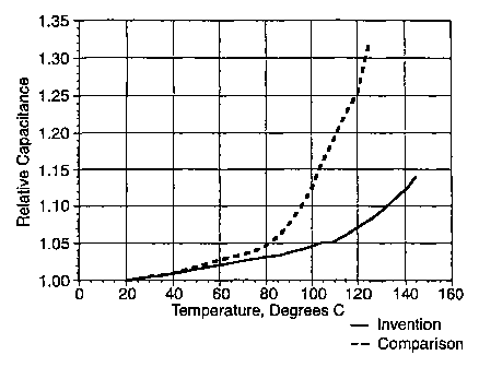
FIG. 1 compares the temperature dependence of capacitance using a 9,9-bis(3-
chloro-4-aminophenyl)fluorene cured epoxy resin formulation and a phenol cured
epoxy
so resin formulation.
CA 02453107 2004-O1-06
WO 03/007319 PCT/US02/17897
FIG. 2 compares the temperature dependence of dissipation factor for a 9,9-
bis(3-
chloro-4-aminophenyl)fluorene cured epoxy resin formulation and a phenol cured
epoxy
resin formulation.
Like reference symbols in the various drawings indicate like elements.
In one aspect, the invention is a dielectric layer that may be used in an
electrical
article, such as a capacitor. Suitable electrical articles are described in
PCT Publication
No. WO 00/45624. The electrical articles described in PCT Publication No. WO
00/45624
generally include a first self supporting substrate having two opposing major
surfaces and
a second self supporting substrate having two opposing major surfaces. A
dielectric layer
to between the first and second substrate provides an electrical insulating
function and
adheres the two substrates.
The dielectric layer of the electrical article, which may be made of one or
more
layers, is made of a polymer. Any polymer may be used that can withstand the
temperatures encountered in a typical solder reflow operation, for example,
180 to 290 °C.
15 Suitable polymeric materials for the dielectric layer include epoxy resins
and blends
thereof. The epoxy resin compositions used to make the dielectric layer in the
electrical
article of the invention include at least one aromatic polyepoxide and at
least one 9,9-
bis(aminophenyl)fluorene (also referred to as "aminophenylfluorene" herein)
curing agent
present in an amount sufficient to provide 0.1 to 1.1 amino groups per epoxy
group present
2o in the aromatic polyepoxide. In this application aromatic polyepoxide means
a molecule
that includes more than one epoxide group, which are attached directly or
indirectly to an
aromatic group. The term epoxy resin composition will be used to refer to an
uncured
composition including an aromatic polyepoxide and a 9,9-
bis(aminophenyl)fluorene
curing agent that can be cured to form a cured epoxy resin.
25 The thermally curable epoxy resin compositions of the invention preferably
include one or more aromatic polyepoxides and one or more 9,9-
bis(aminophenyl)fluorene
curing agents. Preferred aromatic polyepoxides include poly(glycidyl ethers of
polyhydric phenols. Suitable aromatic polyepoxides include the epoxy resins
available
from Shell Chemical Company, Houston, TX, under the trade designation EPON
1001F
3o and EPON 1050. Particularly preferred resins include blends of a
diglycidylether of
bisphenol A and a novolac epoxy, for example, 75 to 90% by weight Epon 1001F
and 25
to 10% by weight Epon 1050F based on the total weight of the resin. A suitable
9,9-
4
CA 02453107 2004-O1-06
WO 03/007319 PCT/US02/17897
bis(aminophenyl)fluorene curing agent for use in the epoxy resin compositions
of the
invention is described in U.S. Patent No. 4,684,678, and has a general Formula
1:
R-
Formula 1
wherein
each R° is independently selected from H, halogen, linear and branched
alkyl groups
having 1-6 carbon atoms, phenyl, nitro, acetyl and trimethylsilyl;
each R is independently selected from H and linear and branched alkyl groups
having 1-6
to carbon atoms; and
each RI is independently selected from R, H, phenyl and halogen.
Preferred curing agents include 9,9 bis(aminophenyl)fluorenes, and 9,9 bis (3-
chloro-4-aminophenyl)fluorene (CAF) and 9,9-bis(3-methyl-4-
aminophenyl)fluorene
(OTBAF) are particularly preferred.
is The 9,9 bis(aminophenyl)fluorene curing agent should be present in the
epoxy
resin composition in an amount sufficient to provide from 0.1 to 1.1 amino
groups, NH-R,
per epoxide group in the aromatic polyepoxide.
When embedded capacitor material is laminated into conventional printed
circuit
boards, lamination temperatures are typically about 175 °C. Lamination
times depend
2o upon the number of lamination cycles required, but are typically more than
about two
hours. However, in some applications, the lamination temperature for
fabrication of a
device containing embedded capacitor material may be higher, about 225
°C, for example.
CA 02453107 2004-O1-06
WO 03/007319 PCT/US02/17897
At this temperature, adhesion between the dielectric layer and the copper
substrate can
become unacceptably low. The composition of the dielectric layer in the
present invention
can be modified to make adhesion loss during extended 225 °C lamination
processes
acceptable. Certain properties, such as adhesion between the dielectric layer
and the
s copper substrate at higher temperatures, may be adjusted by controlling, for
example, the
amount and/or rate of cross-linking in the cured composition. In cases where a
slow cross-
linking reaction is preferred, it may be preferable to reduce the amount of
9,9
bis(aminophenyl)fluorene curing agent present in the epoxy resin composition.
Optionally, other catalysts may be used in the epoxy resin composition such
as, for
to example, amines and imidazoles. Suitable supplementary catalysts are
described in PCT
Publication No. WO 00/45624 and U.S. Patent No. 4,684,678, and preferred
catalysts
include 2,4,6-tris(dimethylaminomethyl)phenol and 5-aminobenzotriazole. Use of
5-
aminobenzotriazole may also improve adhesion between the dielectric layer and
the
substrate layers.
~s In addition, conventional epoxy resin curing agents, such as, for example,
'
polyamines, polyamides, polyphenols and derivatives thereof, may be added to
the epoxy
resin composition in an amount ranging from 10 to 100% by weight, preferably
10 to 50%
by weight of resin. Suitable curing agents include 1,3 phenylenediamine.
The epoxy resin composition may also include conventional additives such as
2o dispersants and solvents. Examples of suitable dispersants include, for
example, a
copolymer of polyester and polyamine, commercially available from Uniqema, New
Castle, DE, under the trade designation HYPERMEER PS3. Examples of solvents
include
methyl ethyl ketone and methyl isobutyl ketone. Other additives, such as
agents to change
viscosity or to produce a level coating, can be used.
2s The epoxy resin composition also preferably includes a plurality of
particles.
Suitable particles are described in PCT Publication No. WO 00/45624, and
include barium
titanate, barium strontium titanate, titanium oxide, lead zirconium titanate,
and mixtures
thereof. A preferred commercially available barium titanate is available from
Cabot
Performance Materials, Boyertown, PA, under the trade designation BT 8. The
particles
3o may be any shape and may be regularly or irregularly shaped. Exemplary
shapes include
spheres, platelets, cubes, needles, oblate, spheroids, pyramids, prisms,
flakes, rods, plates,
fibers, chips, whiskers, and mixtures thereof. The particle size, that is, the
smallest
6
CA 02453107 2004-O1-06
WO 03/007319 PCT/US02/17897
dimension of the particle, typically ranges from 0.05 to 11 Tm, preferably
0.05 to 3.0 Tm,
more preferably 0.05 to 2 Tm. Preferably, the particles have a size allowing
at least two to
three particles to be stacked vertically within the electrically insulating
layer thickness.
The loading of particles in the polymer is typically 20 to 70% by volume,
preferably 30 to 60% by volume, more preferably 40 to 55% by volume, based on
the total
volume of the dielectric layer.
As described in detail in PCT Publication No. WO 00/45624, the particles are
preferably cleaned and dried prior to incorporation into the epoxy resin
composition.
The epoxy resin composition is typically formed by mixing the epoxy resin, the
aminophenylfluorene curing agent, particles, and other optional ingredients.
The resulting
substantially uniform mixture is subsequently coated on a suitable substrate,
then heated
for a time and a temperature sufficient to remove volatile components and cure
the
composition. The resulting cured epoxy resin composition forms the dielectric
layer of the
electrical article. During cure, the aromatic polyepoxide and the
aminophenylfluorene
i5 curing agent react to form a cured epoxy resin having the units of Formula
2:
H IH3 IH
-CHZ CHCHZO ~ ~ ~ OCHzCH-CHz
CH3
Formula 2
2o The preferred cured epoxy resin composition absorbs less than 0.6 weight
percent
moisture over 24 hours time and has a Tg of at least 90 °C. A suitable
test for water
absorption is Test 2.6.2.1 from the IPC-TM-650 Test Methods Manual.
The substrates of the electrical article of the invention may include a single
layer,
or a plurality of layers arranged in a laminate structure. The first and
second substrates
25 may be made of graphite; composites such as silver particles in a polymer
matrix; metal
such as copper or aluminum; combinations thereof, or laminates thereof. A
multilayer
CA 02453107 2004-O1-06
WO 03/007319 PCT/US02/17897
substrate may be made by coating a layer of metal, such as copper or aluminum,
onto a
removable carrier layer. For example, copper layer may be coated onto a
removable
polyester carrier. The first and second substrates may be the same or
different. The
electrical article of the invention may include multiple, interdigitated
insulating and
conductive layers.
A substrate in accordance with the electrical articles of the invention is
preferably
self supporting. The term "self supporting substrate" refers to a substrate
having
sufficient structural integrity such that the substrate is capable of being
coated and
handled. It is preferable that a substrate is flexible; however, rigid
substrates may also be
io used.
Typically, the major surface of the first substrate in contact with the
electrically
insulating layer and the major surface of the second substrate in contact with
the
electrically insulating layer are electrically conductive when forming a
capacitor. Surface
treatment, which adds material to these major surfaces by, for example,
oxidation or
~5 reaction with a coupling agent, may be used to promote adhesion.
Alternatively, a separate
coating step may be performed to apply an adhesion promoting primer, such as 5-
aminobenzotriazole. Treatment of the substrate surface with 5-
aminobenzotriazole may be
particularly relevant for copper foils not having a chromate anti-tarnish
surface treatment.
The resulting material on the major surface of the substrate itself may not
necessarily be
2o conductive, but a capacitor is formed provided the substrates themselves
are conductive.
Preferably, a substrate has a thickness ranging from 0.5 to 3 mils
(approximately
to 80 Tm), more preferably 0.5 to 1.5 mils (approximately 10 to 38 Tm).
When the substrate is a metal, the metal preferably has an anneal temperature
which is at or below the temperature for curing the electrically insulating
layer, or the
25 metal is annealed before the electrically insulating layer is coated.
A preferred substrate is copper. Exemplary copper includes copper foil
available
from Carl Schlenk, AG, Nurnberg, Germany.
A method for manufacturing an electrical article of the invention, which is
described in detail in PCT Publication No. WO 00145624, includes providing a
first
3o substrate having two opposing major surfaces. An epoxy resin composition
may then be
coated onto a first major surface of the first substrate. A second substrate,
having two
opposing major surfaces, is laminated to the epoxy resin composition on the
first major
CA 02453107 2004-O1-06
WO 03/007319 PCT/US02/17897
surface of the first substrate. The resulting laminate is then heated for a
time and a
temperature sufficient to cure the epoxy resin composition.
Alternatively, the second substrate may also include an epoxy resin
composition on
its first major surface and the first .and second substrates may be laminated
together to
connect the first major surface of each of the first and second substrate,
that is, the epoxy
resin coated side of each substrate may be laminated together.
The major surfaces of the substrates are preferably substantially free of
debris or
chemisorbed or adsorbed materials to maximize adhesion with the electrically
insulating
layer. Exemplary methods are described in PCT Publication No. WO 00145624 and
to include treating with an argon-oxygen plasma or with an air corona, or wet
chemical
treatment. Particulates adhering to both sides of the substrate can be removed
using, for
example, an ultrasoniclvacuum Web cleaning device commercially available for
Web
Systems Inc., Boulder, CO, under the trade designation ULTRACLEANER.
Alternatively, the substrate may be cleaned using a tacky roller system such
as
is manufactured by Polymag Tech of Rochester, NY. Preferably, the substrate is
not
scratched, dented, or bent during this surface treatment step in order to
avoid possible
coating problems and coating defects which may result in non-uniform coating
or shorted
articles, such as shorted capacitors.
If a mixture of an aminophenylfluorene and a phenol catalyst is used, metal
2o substrates, such as copper foils that have no chromate anti-tarnish surface
treatment, may
require a separate coating step to apply an adhesion promoting primer such as,
for example
5-aminobenzotriazole. Preferably, the phenol catalyst is entirely eliminated
and replaced
with 5-aminobenzotriazole, which provides a reduced cure time and eliminates
the
separate priming step. With this formulation, it is possible, using the same
process, to use
2s copper foils having a chromate anti-tarnish surface treatment and foils
having no anti-
tarnish treatment.
The cleaned copper foil may be coated with the epoxy resin composition using
any
suitable method, for example, a gravure coater. The resin composition is then
dried to
remove residual solvent. The dry thickness of the coated epoxy resin
composition depends
30 on the percent solids in the composition, the relative speeds of the
gravure roll and the
coating substrate, and on the cell volume of the gravure used. Typically, to
achieve a dry
thickness in the range of 0.5 to 2 Tm, the percent solids in the epoxy resin
composition are
CA 02453107 2004-O1-06
WO 03/007319 PCT/US02/17897
20 to 75 % by weight. The coating is preferably dried to a substantially tack-
free state in
the oven of the coater, typically at a temperature of less than about 100
°C. More
preferably, the coating is dried in stages starting with a temperature of
about 30 °C and
ending with a temperature of about 100 °C, and then wound onto a roll.
Higher final
s drying temperatures, for example, up to about 200 °C can be used, but
are not required.
Generally, very little cross-linking occurs during the drying step; its
purpose is
primarily to remove as much solvent as possible. Retained solvent may lead to
blocking
(that is, unwanted interlayer adhesion) when the coated epoxy resin
composition is stored
on a roll and to poor adhesion for the laminate. More specifically, if there
is residual
o solvent in the coating, or if the copper foil is uneven, there can be
tendency for a small
portion of the coating to stick to the opposite side of the foil on the
adjacent wrap, leaving
a pinhole-like defect in the coating (referred to as "pick-ofd'). This defect
can cause a
direct short, or premature breakdown under an applied voltage.
Aminophenylfluorene
catalyzed epoxy resin composition coatings are considerably less prone to this
defect than
i5 are epoxy coatings catalyzed by phenol catalysts.
Coating techniques to avoid defects include in-line filtration and deaeration
(to
remove air bubbles) of the coating mixture. In addition, it is preferable,
before laminating
two substrates coated with a dielectric layer, that at least one of the
dielectric layers is
partially cured, preferably in air. In particular, adhesion of the substrate
may be improved
2o by heat treating the coating before lamination. The time for heat
treatment~is preferably
short, for example, less than about 10 minutes, particularly at higher
temperatures.
Lamination is preferably carried out using two of the coated substrates
described
above. One of the coated substrates may go through an oven or over a heated
roller before
reaching the laminator, for example, at a temperature ranging from 125 to 175
°C for less
25 than 30 seconds, and more preferably at a temperature 125 to 160 °C.
This preliminary
heating step can be done on one or both of the coated substrates. To make an
electrical
article of the present invention, the coated substrates may be laminated,
dielectric layer to
dielectric layer, using a laminator with two nip rollers heated to a
temperature ranging
from 120 to 200 °C, preferably about 135 °C. Suitable air
pressure is supplied to the
30 laminator rolls, preferably at a pressure ranging from 5 to 40 psi (34 to
280 kPa),
preferably about 15 psi (100 kPa). The roller speed can be set at any suitable
value and
preferably ranges from 12 to 36 inches/minute (0.5 to 1.5 cm/second), more
preferably
CA 02453107 2004-O1-06
WO 03/007319 PCT/US02/17897
about 15 inches/minute ( 0.64 cm/second). This process can be conducted in a
batch mode
as well.
The laminated material can be cut into sheets of the desired length or wound
onto a
suitable core.
The laminated material is then heated for a sufficient time and temperature to
cure
the epoxy resin composition. Exemplary curing temperatures include
temperatures
ranging from 150 to 225 °C, preferably 160 to 200 °C, and
exemplary curing times include
a period ranging from 90 to 180 minutes, preferably 90 to 120 minutes.
Adhesion of the dielectric layer to a metal substrate may be enhanced if the
metal
to is sufficiently soft at the time of coating or becomes soft during
lamination and/or cure;
that is, the foil is annealed before coating or becomes annealed during
subsequent
processing. Annealing may be accomplished by heating the substrate before the
coating
step or as a result of the curing or drying step if the metal anneal
temperature is at or lower
than the cure temperature of the epoxy resin composition. It is preferred to
use a metal
~5 substrate with an anneal temperature below the temperature at which curing
occurs.
Annealing condition will vary depending on the metal substrate used.
Preferably, in the
case of copper, at either of these stages in the process, the metal substrate
obtains a
Vickers hardness, using a 10 g load, of less than about 75 kg/mm2. A preferred
temperature range of copper to achieve this hardness ranges from 100 to 180
°C, more
2o preferably 120 to 160 °C.
Subsequent to cure, the force required to separate the first and second
substrates of
the electrical article at a 90 degree peel angle is greater than about 3
pounds/inch (about
0.5 kiloNewtons/meter (kN/m)), preferably greater than 4 pounds/inch (0.7
kN/m), more
preferably greater than 6 pounds/inch ( 1 kN/m), as measured according to the
IPC Test
25 Method Manual, IPC-TM-650, test number 2.4.9 dated October 1988, as
published by the
Institute for Interconnecting and Packaging Electronic Circuits. If more than
two
substrates are present in an electrical article of the present invention, this
force is required
to separate any pair of substrates separated by an electrically insulating or
electrically
conducting layer.
so Although an electrical article of the present invention can be functional
as it is
fabricated, the electrical article may preferably be patterned as described
below, for
example, to form discrete islands or removed regions in order to limit lateral
conductivity.
11
CA 02453107 2004-O1-06
WO 03/007319 PCT/US02/17897
The patterned electrical article may be used as a circuit article itself or as
a component in a
circuit article, as described below.
A surface of the first or second substrate of the electrical article that is
accessible
may be contacted, for example, by an electrical trace, to make electrical
contact so that the
first or second substrate acts as an electrode. In addition, it may be
desirable to make
electrical contact with the major surface of the first or second substrate in
contact with the
dielectric layer or to provide a through hole contact. Through hole contacts
are useful
when no interaction with the electrical device is desired. In order to reach
the major
surface of the first or second substrate in contact with the dielectric layer
or to provide a
1o through hole contact, the electrical article may be patterned.
Any suitable patterning technique known in the art may be employed. Suitable
patterning techniques are described in PCT Publication No. WO 00145624.
The electrical article of the present invention itself may function as a
circuit article,
with some modification. In one instance, the electrical article may be
patterned. Tn this
~s instance, a circuit article may be prepared by providing an electrical
article of the present
invention and patterning the electrical article as described above to provide
a contact for
electrical connection. Either one or both sides of the electrical article are
patterned to
allow access to each major surface of the first and second substrates and to
provide a
through hole contact.
2o In another embodiment, a circuit article may be prepared by a method
comprising
the steps of providing an electrical article of the present invention,
providing at least one
electrical contact, and connecting the contact to at least one substrate of
the electrical
article.
An electrical article of the present invention may further comprise one or
more
2s additional layers, for example, to prepare a PWB or flexible circuit. The
additional layer
may be rigid or flexible. Exemplary rigid layers include fiberglass/epoxy
composite
commercially available from Polyclad, Franklin, NH, under the trade
designation PCL-
FR-226, ceramic, metal, or combinations thereof. Exemplary flexible layers
comprise a
polymer film such as polyimide or polyester, metal foils, or combinations
thereof.
Polyimide is commercially available from DuPont under the trade designation
I~APTON
and polyester is commercially available from 3M Company (3M), St. Paul, MN,
under the
trade designation SCOTCHPAR. These additional layers may also contain
electrically
12
CA 02453107 2004-O1-06
WO 03/007319 PCT/US02/17897
conductive traces on top of the layer or embedded within the layer. The term
electrically
conductive traces refers to strips or patterns of a conductive material
designed to carry
current. Suitable materials for an electrically conductive trace comprise
copper,
aluminum, tin, solder, silver paste, gold, and combinations thereof.
In this embodiment, a preferred method of making a circuit article comprises
the
steps of providing an electrical article of the present invention, patterning
at least one side
of the electrical article, providing an additional layer, attaching the layer
to the electrical
article, and providing at least one electrical contact to at least one
substrate of the
electrical article. Preferably, a second additional layer is provided and
attached to the
to electrical article.
An electrical article of the present invention can be used in a PWB, for
example, a
flexible circuit, as a component, which functions as a capacitor. The
capacitance of the
article at 125 °C is within 15% of the room temperature value and has a
leakage current at
85 °C and 85% relative humidity less than 100nA using a 6 volt bias.
~s The electrical article may be embedded or integrated in the PWB or flexible
circuit. Methods for manufacturing a flexible circuit or PWB using the
electrical article of
the present invention are described in PCT Publication No. WO 00145624 and are
cited
herein by reference.
The present invention also encompasses an electrical device comprising an
2o electrical article of the present invention functioning in an electrical
circuit of a circuit
board (PWB) or a flexible circuit. The electrical device may include any
electrical device
which typically employs a PWB or flexible circuit having a capacitive
component.
Exemplary electrical devices include cell phones, telephones, fax machines,
computers,
printers, pagers, and other devices as recognized by one skilled in the art.
The electrical
25 article of the present invention is particularly useful in electrical
devices in which space is
at a premium or that operate at frequencies greater than 1 GHz.
This invention is illustrated by the following examples, but the particular
materials
and amounts thereof recited in these examples, as well as other conditions and
details
should not be construed to unduly limit this invention.
13
CA 02453107 2004-O1-06
WO 03/007319 PCT/US02/17897
EXAMPLES
Example 1: Electrical Article with (Aminophenyl)fluorene Cured Electrically
Insulating Layer Containing 5-Aminobenzotriazole
Com onent Grams
E on 1001F+Epon 1050 16.0
9,9-bis(3-chloro-4-aminophenyl)fluorine 4.0
Barium titanate, 0.2 ~,m (Cabot Performance 78.7
Materials)
PS3 polyester/polyamine copolymer dispersant 1.3
(Uni ema)
5-aminobenzotriazole 0.08
The above dispersion was coated onto copper foil ( 1 ounce foil, 35 ~,m thick)
using
a gravure or die coating technique. The dispersion can be coated on untreated
copper foil
without the necessity of a separate priming step. Dry thicknesses of the
dielectric ranged
from approximately 2.0 to 5.0 ~,m. The coating was dried to a tack-free
surface, then
to wound into rolls. Two rolls were subsequently laminated, coated side to
side, using two
heated nip rollers. A standard photoresist laminator works well for small
samples. The
is
laminated material was cured at 180 °C for approximately 1.5 to 2
hours. The cured
panels were then patterned on one or both sides using conventional photoresist
and etchant
to produce individual capacitors.
Example 2: Electrical Article with (Aminophenyl)fluorene Cured Electrically
Insulating Layer Containing 2,4,6-Tris(dimethylaminomethyl)phenol
Com onent Gramsa Grams
E on 1001F a oxy (Shell Chemical) 20.2 16.2
E on 1050 a oxy (Shell Chemical) 5.0 4.0
9,9-bis(3-chloro-4-aminophenyl)fluorene0 5.1
(CAF)
Barium titanate, 0.2 ~.m 100 100
(Cabot Performance Materials)
PS3 polyester/polyamine copolymer 1.8 1.8
dispersant
(Uni ema)
Methyl ethyl ketone/methyl isobutyl127 127
ketone (4:6)
2,4,6-tris(dimethylaminomethyl)phenol0.25 0.025 or
0
2o a Standard formulation using only 2,4,6-tris(dimethylaminomethyl)phenol
catalyst as the
curing agent. b 9,9-bis(3-methyl-4-aminophenyl)fluorene (OTBAF) was also used.
14
CA 02453107 2004-O1-06
WO 03/007319 PCT/US02/17897
The above dispersions were coated onto copper foil (1 ounce foil, 35 ~,m
thick)
using a gravure or die coating technique. Adhesion promoting agents such as 5-
aminobenzotriazole may be coated onto the substrate prior to coating by the
epoxy.
Typically a dilute solution, for example, 0.05 to 0.15% by weight in an
alcohol such as
methanol, is applied by standard coating techniques and the substrate dried.
Dry
thicknesses of the dielectric ranged from approximately 2.0 to 5.0 ~.m. The
coating was
dried to a tack-free surface, then wound into rolls. Two rolls were
subsequently
laminated, coated side toside, using two heated nip rollers. A standard
photoresist
laminator works well for small samples. The laminated material was cured at
180 °C for
approximately 2 hours. The cured panels were then patterned on one or both
sides using
conventional photoresist and etchant to produce individual capacitors.
The temperature dependence of capacitance and dissipation factor is shown in
Figure 1 and Figure 2. The leakage current was measured by subjecting the
capacitor to a
voltage bias in an 85 °C, 85% relative humidity environment. For
example, when a
~5 capacitor with the standard formulation was subjected to a 6 volt bias
under these
conditions, the leakage current was 100 nA/cm2. A similar capacitor with the
aminophenylfluorene crosslinked epoxy had a leakage current of only IO nA/cm2,
an order
of magnitude improvement.
2o Example 3: Capacitor with (Aminophenyl)fluorene Cured Electrically
Insulating
Layer Containing 5-Aminobenzotriazole for High Temperature Applications
Component Sample A Sample B
Grams Grams
Epon 1001F + Epon 1050 epoxy (Shell16.0 16.8
Chemical)
9,9-bis(3-chloro-4-aminophenyl)fluorine4.0 3.2
(CAF)
Amine equivalent/epoxy equivalent 1:1 0.6:1
ratio
Barium Titanate 78.7 78.7
PS3 polyester/polyamine copolymer 1.3 1.3
dispersant
(Uniqema)
5-aminobenzotriazole catalyst 0.08 0
CA 02453107 2004-O1-06
WO 03/007319 PCT/US02/17897
Component Sample Sample B
A Grams
Grams
Initial cure temperature, C 180 225
Adhesion after initial cure, lbs/inch4.4 3.4
Adhesion after 6 hours at 225 C, 2.0 4.0
lbs/inch
This example compares two panels made with the same raw materials, but with
changes in the ratio of fluorene compound to epoxy, presence of a catalyst,
and the initial
cure temperature. The above dispersions were coated onto copper foil (1 ounce
foil, 35
s ~.m thick) using a gravure or die coating technique. The dispersion can be
coated on
untreated copper foil without the necessity of a separate priming step. Dry
thicknesses of
the dielectric ranged from approximately 2.0 to 5.0 ~,m. The coating was dried
to a tack-
free surface, then wound into rolls. Two rolls were subsequently laminated,
coated side to
side, using two heated nip rollers. A standard photoresist laminator works
well for small
to samples. The laminated materials were cured at either 180 °C (Sample
A) or 225 °C
(Sample B) for approximately 1.5 to 2 hours. The cured panels were then
patterned on
one or both sides using conventional photoresist and etchant to produce
individual
capacitors. Adhesion was measured using a 90 degree peel strength as described
above.
A number of embodiments of the invention have been described. Nevertheless, it
15 will be understood that various modifications may be made without departing
from the
spirit and scope of the invention. Accordingly, other embodiments are within
the scope of
the following claims.
16