Note: Descriptions are shown in the official language in which they were submitted.
CA 02454446 2004-O1-19
WO 03/012855 PCT/US02/24112
METHOD AND APPARATUS FOR FABRICATING MERCURIC IODIDE
POLYCRYSTALLINE FILMS FOR DIGITAL RADIOGRAPHY
STATEMENT REGARDING FEDERALLY SPONSORED RESEARCH OR
DEVELOPMENT
This invention was made with government support received from National
Institute of Health, Grant # 1R43GM62069. The Government has certain rights in
this
invention.
FIELD OF THE INVENTION
This invention is related to digital radiography, and particularly to a method
and
apparatus for fabricating mercuric iodide (HgI2) polycrystalline films for
digital
radiography applications.
BACKGROUND OF THE INVENTION
Traditionally, photographic films have been used to perform X-ray imaging.
Photographic film techniques have the advantages of good spatial resolution
(better than
50 ~,m) and very large active areas. However, use of photographic films
suffers from
many drawbacks, including low X-ray detection efficiency, non-linearity, and
slow image
retrieval processes.
Thus, there currently is a growing interest in developing digital radiographic
detectors for medical, scientific and industrial applications. The
applications for digital
radiographic detectors may include medical diagnostic applications, non-
destructive
evaluation of materials, X-ray diffraction of biological and other material
samples, and
astronomical observations. For example, some estimates indicate that, in the
medical
area alone, there are over 600 X-ray images produced per 1000 population per
year, much
of which may be performed using digital radiographic techniques.
Digital techniques in radiology typically have several benefits over
traditional X-
ray film analog methods. These include reduced radiation dose for an
equivalent image,
convenient image acquisition and retrieval (avoiding film development time and
cost),
1
CA 02454446 2004-O1-19
WO 03/012855 PCT/US02/24112
digital image processing (image enhancement), computer-assisted diagnosis, and
easy
image storage and transmission. Furthermore, the ability to provide real time
images may
be advantageous in some applications.
Recently, amorphous silicon (a-Si:H) transistor-addressed arrays (amorphous
silicon arrays) have become a leading technology for large area flat panel
imaging.
Imagers with up to 2304 x 3200 pixels (29.2 x 40.6 cm2) on a single substrate
with pitch
of 127 ~m have been produced, and several companies have started commercial
production of the amorphous silicon arrays. Smaller area but higher spatial
resolution X
ray imagers are also produced using single crystal silicon CMOS readout
technology.
The sensitivity to X-rays is obtained by coupling a phosphor screen to either
the
amorphous silicon array or the CMOS readout. Typically Gd202S:Tb phosphor is
deposited on the amorphous silicon array-based imagers, although CsI:TI has
also been
used.
The detectors utilizing phosphors can be characterized as indirect detectors,
which
typically require a combination of processes to achieve an image. First,
transfer of the X-
ray energy into visible light photons by the phosphor should be accomplished,
and then
subsequently the light should be converted into electrical signals using light
sensitive
readout arrays.
Although indirect detection may be an improvement over the conventional analog
technique using photographic films, this approach may suffer from deficiencies
including
low efficiency of the energy transfer and limited spatial resolution due to
light spreading
in the phosphor. The poor energy transfer is due to an inefficient process of
creating and
collecting visible light photons. The increased light spread is a consequence
of increasing
phosphor thickness to achieve better efficiency in stopping X-rays. The
increased light
spread can be ameliorated by use of specially grown CsI scintillators with a
columnar
structure when the X-rays have low energies and/or the CsI scintillators have
thin layers.
However, as soon as the aspect ratio (the length of the column to the
diameter) increases
(e.g., to account for increase in X-ray energies), the light collection within
the scintillator
columns decreases, further reducing the energy transfer efficiency.
2
CA 02454446 2004-O1-19
WO 03/012855 PCT/US02/24112
Therefore, it is desirable to provide a digital X-ray detector that can
provide
efficient energy detection over a wide range of X-ray intensities and improved
spatial
resolution over phosphor-based digital X-ray detectors.
SUMMARY
In an exemplary embodiment according to the present invention, a method is
provided for fabricating a polycrystalline film in a thermal evaporation
system. The
polycrystalline film is capable of directly detecting radiation. The method
includes
placing source material in a container; evacuating the container to create
vacuum within
the container; and heating the source material to evaporate the source
material, wherein
the evaporated source material is deposited on a substrate. The
polycrystalline film is
used in as deposited form to detect the radiation.
In another exemplary embodiment according to the present invention, a thermal
evaporation system for fabricating a polycrystalline film is provided. The
polycrystalline
film is capable of directly detecting radiation. The system includes a
container adapted
for creating vacuum within and for heating source material disposed therein; a
furnace
enclosing at least a portion of the container, the furnace being capable of
heating the
container to evaporate the source material; a substrate holder for holding the
substrate, on
which the evaporated source material is deposited for growth of the
polycrystalline film;
and a temperature controlling system for maintaining the source material and
the substrate
at respective predetermined temperature ranges to control a growth rate of the
polycrystalline film.
In yet another exemplary embodiment according to the present invention, a
radiography system is provided. The radiography system includes an array
detector
capable of receiving radiation and generating corresponding electrical signal,
the array
detector comprising a polycrystalline film fabricated through sublimation on a
readout
substrate, wherein the polycrystalline film is used in as deposited form after
being grown
on said readout substrate; and an image processor coupled to the array
detector to
generate a displayable image from the electrical signal.
3
CA 02454446 2004-O1-19
WO 03/012855 PCT/US02/24112
BRIEF DESCRIPTION OF THE DRAWINGS
These and other aspects of the invention may be understood by reference to the
following detailed description, taken in conjunction with the accompanying
drawings,
which are briefly described below:
FIG. 1 is a schematic drawing of a thermal evaporation system, which may be
used to fabricate HgI2 polycrystalline films in an embodiment according to the
present
invention;
FIG. 2 is a graph illustrating correlation between grain size and substrate
temperature for polycrystalline HgI2 film grown by thermal evaporation in an
embodiment according to the present invention;
FIG. 3 illustrates X-ray diffraction diagrams for films grown at different
substrate
temperature in an embodiment according to the present invention;
FIG. 4 is a graph illustrating polycrystalline HgI2 film textures as function
of
substrate temperature in an embodiment according to the present invention;
FIG. 5 illustrates a set up for measuring thickness of polycrystalline HgI2
films in
an embodiment according to the present invention;
FIG. 6 is a graph illustrating thickness of HgI2 required for 99% stopping of
X-ray
energy and percentage stopping for a SOO~,m HgI2 film;
FIG. 7 is a graph illustrating dark current density versus detector bias for
several
detectors and films;
FIG. 8 is a graph illustrating a voltage pulse from a polycrystalline HgI2
film in an
embodiment according to the present invention measured with a fast-rise time
pre-
amplifier as collected by a digital oscilloscope;
FIG. 9 is a graph illustrating X-ray response linearity for different kV at X-
ray
tube;
FIG. 10 is a graph illustrating X-ray sensitivity measurements in an
embodiment
according to the present invention;
FIG. 11 is a block diagram of a digital radiography system, in which an
exemplary
embodiment according to the present invention may be applied;
FIG. 12 is a detailed block diagram of the digital radiography system of FIG.
11;
4
CA 02454446 2004-O1-19
WO 03/012855 PCT/US02/24112
FIG. 13 is a block diagram of a digital radiography system, in which an
exemplary
embodiment according to the present invention may be applied; and
FIG. 14 is a block diagram of a digital radiography system with an amorphous
silicon TFT readout in which an exemplary embodiment according to the present
invention may be applied.
DETAILED DESCRIPTION
In an exemplary embodiment according to the present invention, a method and
apparatus for fabricating polycrystalline film-based digital X-ray detectors
are provided.
The polycrystalline film-based digital X-ray detectors are used for efficient
detection of
X-ray images at high spatial resolution.
Polycrystalline films axe grown through sublimation of a source material on
substrates such as silicon and alumina. The source material used may be highly
purified
HgI2 in powder form. Other metallic iodides such as lead iodide (PbI2) may
also be used
as the source material to produce other types of polycrystalline films. The
source material
in a glass ampoule is evaporated onto a substrate using a furnace of a thermal
evaporation
system. The substrate may comprise amorphous silicon with a TFT (thin film
transistor)
array or a CMOS (complementary metal-oxide semiconductor) axray fabricated
thereon.
These arrays may be used as readout arrays when the polycrystalline film is
used in a
digital X-ray detector for direct detection of X-rays without using a phosphor
screen.
The thickness of the grown layers, size of the grains and crystallinity can be
regulated in a controlled way over a wide range without the need for heat-
treating (e.g.,
sintering) the layers after growth by adjusting the growth parameters such as
Tsource~
Tsubscrate~ source-substrate distance, and growth rate in specific
reproducible ways. Thus,
the polycrystalline films may be used in "as deposited" form to detect
radiation. Detectors
made from these films typically give dark current densities in the order of a
few pA/cm2
up to several hundred pA/cm2 (pico amps/cm2) and apparent resistivities in the
order of
101° to 1014 Ohms-cm. X-ray sensitivity results also show these
detectors have good
performance. For example, low dark current, good sensitivity and linearity of
the response
to X-rays allow HgI2 polycrystalline layers to be used in digital X-ray
imaging systems.
5
CA 02454446 2004-O1-19
WO 03/012855 PCT/US02/24112
The deficiencies associated with indirect detection may be minimized or
eliminated through the use of direct conversion detectors in an embodiment
according to
the present invention. Thin polycrystalline films of high atomic number (high
Z) and
high-density semiconductor material can effectively absorb the incoming X-ray
radiation
and convert it directly into electrical signals, which can be read by
associated readout
arrays.
The efficiency of the energy transfer from X-rays to electrical signal can be
an
order of magnitude larger in the direct detection approach than in the case of
indirect
detection using phosphors due to the basic underlying physics. That is, the
mean energy
for creation of an electron-hole pair in a semiconductor detector is typically
an order of
magnitude lower than the corresponding energy necessary to generate the same
signal
through the scintillation approach. This results in a larger signal for the
same incoming
X-ray event for the direct detector approach.
The direct detector approach can significantly improve detective quantum
efficiency (DQE) despite the fact that indirect detectors can achieve DQE as
high as 60
SO percent. DQE values are usually quoted for very high intensities of
incident X-ray
photons (photon limited case). DQE is a function of the number of photons
interacting
with the detector and drops significantly at lower X-ray intensities. Although
DQE
improves with the polycrystalline semiconductor converters compared to other
technologies for the whole range of the incident X-ray intensities, the DQE
improves the
most at lower X-ray intensities. More efficient energy conversion and better
signal-to-
readout noise would allow direct detection to result in better detecting
method.
The improved DQE at lower intensities may be important for applications such
as
fluoroscopy, where the dynamic temporal aspect of the measurement favors
shorter
measurement times. Another important consideration for direct detectors is
that the
charges generated by X-rays do not spread laterally (aside from negligible
spreading due
to diffusion) but move instead along the applied electric field lines.
Spreading of the light
in the indirect scintillator approach is a well-known factor causing
deteriorated spatial
resolution. Thus, the direct approach offers better spatial resolution than
the indirect
6
CA 02454446 2004-O1-19
WO 03/012855 PCT/US02/24112
approach. It also allows for construction of thicker, more efficient detectors
without any
loss in resolution due to lateral spread in the detector.
Several high Z amorphous and polycrystalline semiconductor materials may be
used for this application including thallium bromide (TIBr), amorphous
selenium (a-Se),
lead iodide (PbI2), cadmium zinc telluride (CdZnTe), and mercuric iodide
(HgI2). Of
these, HgI2 polycrystalline films should be used for X-ray converters due to
basic
characteristics of the material.
HgI2 may offer the most efficient energy transfer due to high X-ray stopping
power and low mean energy required for electron-hole pair generation, low dark
currents,
and good long-term stability with a proper surface passivation. The remaining
parameters, including mobility lifetime product for electrons and holes are
among the
highest of all of the candidate materials. In addition, HgI2 can be easily
deposited by low
temperature thermal evaporation without altering its stoichiometry during the
sublimation
process.
Before the polycrystalline film is grown on a substrate, the source material
should
be purified so that the growth process may use the purest possible source
material. For
example, in an exemplary embodiment according to the present invention, the
polycrystalline film is grown using mercuric iodide (HgI2) powder with
impurity
concentration of major active contaminants of less than approximately 10 parts
per
million (PPM). In this embodiment, to purify the HgI2 used for growth of the
polycrystalline films, the starting compounds including mercury and iodine,
such as, for
example, mercuric chloride (HgClz) and potassium iodide (I~, respectively,
should be
highly purified.
Then the HgI2 should be synthesized using the highly purified starting
compounds
(e.g., HgCl2 and KI). In other embodiments, source compounds other than HgCl2
and KI
may be purified, then used to synthesize HgI2. An exemplary process for
preparation of
HgIz is disclosed in N.L. Skinner et al., "Preparation and Evaluation of
Mercuric Iodide
for Crystal Growth," Nucl. Instr. & Meth. A283 (1989) pp. 119-122, the
contents of
which are fully incorporated by reference herein.
Then HgI2 may be purified through the "4XMS" process disclosed in H.A.
7
CA 02454446 2004-O1-19
WO 03/012855 PCT/US02/24112
Lamonds, "Review of Mercuric Iodide Development Program in Santa Barbara,"
Nucl.
Instr. & Meth. 213 (1983) pp. 5-12, the contents of wluch are fully
incorporated by
reference herein. The "4XMS" purification process includes HgI2 vacuum
sublimation
under continuous evacuation, then thermal breakdown and coalescing of
impurities in the
molten HgI2 when the HgIz is melted and then cooled, and finally filter
sublimation under
vacuum in a closed system. The filtering sublimation, for example, may be
through a
ceramic frit in an evacuated and sealed glass tube.
Separation between HgI2 and the impurities occurs during vaporization because
different materials vaporize at different temperatures. For example, HgI2
vaporizes at
lower temperature than most impurities in this case. Further, some impurities
coalesce
and form larger particles than HgI2, and so they don't make it through the
ceramic frit.
In other embodiments, other processes known to those skilled in the art may be
used to purify the source compounds and the synthesized HgI2. In still other
embodiments, other metallic iodides, such as, for example, lead iodide PbI2 or
other
suitable high Z amorphous and/or polycrystalline semiconductor materials may
be used to
fabricate the polycrystalline filin on a substrate. In each case, highly
purified
stoichiometric molecules are formed, and then sublimed to grow the
polycrystalline film
on a substrate.
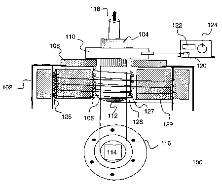
FIG. 1 is a schematic drawing of a thermal evaporation system 100, which may
be
used to grow polycrystalline films, such as, for example, HgI2 polycrystalline
films, in an
exemplary embodiment according to the present invention, using a thermal
evaporation
method. The thermal evaporation system 100 includes a furnace 102, which is
used to
heat up source material 112 (e.g., HgI2 powder) for evaporation through
sublimation to
grow polycrystalline films on a substrate 114. An ampoule (bell jar) 106,
which may be
made of Pyrex glass, is used to contain ~ the source material 112, which
should be .in
powder form.
Vacuum 118 is applied to the ampoule after loading the source material 112 but
before the growth process takes place. The furnace should be temperature
controlled
within a predetermined range of temperatures. Prior to and during the growth
process,
the ampoule 106 is sealed so that the vacuum is maintained within the ampoule.
The
8
CA 02454446 2004-O1-19
WO 03/012855 PCT/US02/24112
sealed ampoule 106 should not contain undesirable impurities, such as, for
example,
organic based (carbon-based) and metallic based materials.
The substrate 114 may be fabricated from silicon, alumina, glass or other
suitable
materials, and may contain circuitry for electronic readout of the x-ray
produced signals.
When the alumina substrate is used, it may be thinly coated with palladium to
provide
metal contacts. In a further embodiment the contact and the HgI2 may have a
blocking
barrier formed between them by coating the contact with a thin layer of an
insulator
material such as "parylene" in order to control the flow of current between
the HgI~ and
the contact and to prevent chemical reaction between the HgI2 and the contact.
In one
exemplary embodiment, said insulator layer is deposited over the entire
substrate
containing the contact.
The ampoule 106 should be mounted such that its opening surrounds a substrate
holder and cooler 104, which is used to hold the substrate 114. The surface of
the
substrate holder and cooler 104 which interfaces with the substrate may, for
example,
comprise Teflon~. Teflon~ is a registered trademark of E.I. du Pont de Nemours
and
Company, a Delaware corporation having a place of business at 101 West 10th
St.,
Wilmington, DE 19898. The cross section 116 illustrates the substrate 114 held
in place
by the substrate holder and cooler 104 situated at the opening of the ampoule
106, which
abuts a top holder 110. The top holder 110, for example, may be made of
stainless steel.
The substrate temperature controller 122 should be used to control the
temperature of the substrate 114 to be at a predetermined temperature or
witlun a range of
predetermined temperatures by controlling the temperature of the substrate
holder and
cooler 104. A digital thermometer 120 may be used to monitor the temperature
of the
substrate 114, and may provide feedback control capability to the substrate
temperature
controller 122. The top holder 110 holds the substrate holder and cooler 104
over the
fiunace 102, and an insulator 108 keeps the stainless steel holder 110
substantially
insulated from the furnace 102.
In another exemplary embodiment according to the present invention, an
additional heating element 128 is situated at the outside of the growth
ampoule 106. The
heating element may have a resistive device separating elements 126 and
thermocouples
9
CA 02454446 2004-O1-19
WO 03/012855 PCT/US02/24112
127 placed at various points in the furnace and/or on the ampoule 106 in order
to control
and maintain a fixed three-dimensional temperature profile within the growth
ampoule
106.
A thermocouple switch may be used to switch between different thermocouples to
monitor temperatures. In an embodiment where there are multiple digital
thermometers
each for measuring different thermocouple temperatures at various places in
the furnace,
the thermocouple switch 124 may not be needed.
It should be noted that in this and other embodiments, the process of
fabricating
polycrystalline films (e.g., HgI2 films) are completed upon growth of the film
through the
evaporation process in the thermal evaporation system of FIG. 1. In other
words, in these
embodiments of the present invention, no further post-deposit processing on
the
polycrystalline film, such as, for example, heat-treatment (e.g., sintering)
to form a single,
coherent, continuous coherent film, is required or used to produce the X-ray
sensitive
digital detector. Further insulation and ambient temperature and environmental
controls
may be used in other embodiments.
In preparation for filin growth, the substrates may be coated with a thin
layer of
palladium on one side to serve as the rear electrical contact to the
polycrystalline film. In
embodiments wherein the polycrystalline film is grown on readout arrays, such
as, for
example, TFT arrays on amorphous silicon or CMOS arrays, palladium coating may
not
be needed since these readout arrays typically already contain metal (e.g.,
palladium (Pd),
Indium Tin Oxide (ITO), or Titanium Tungsten (TiW)) contacts. In certain
embodiments
the contact and the HgI2 may.have a blocking barrier formed between them by
coating the
contact with a thin layer of an insulator material such as "parylene" in order
to control the
flow of current and to partially isolate the HgI2 from the contact. In one
exemplary
embodiment, said insulator layer is deposited over the entire substrate
containing the
contact.
The prepared (e.g., palladium coated) substrates are mounted in the substrate
holder and cooler 104 as seen in the cross sectional illustration 116 of FIG.
1. The
ampoule 106, which may also be referred to as a growth ampoule, should be
loaded with
the source material 112 (e.g., high purity grade mercuric iodide (HgI2) in
powder form)
CA 02454446 2004-O1-19
WO 03/012855 PCT/US02/24112
and evacuated to, for example, between 10-5 and 10-~ Torr and more
particularly, between
SxlO-5 and SxlO-6 Torr.
Prior to loading the source material, the growth ampoule should be cleaned
with
aqua regia or other suitable cleanser, rinsed with distilled water, and then
baked for 12
hours at 300 °C. The baking should remove moisture and/or other
impurities remaining
in the ampoule. In other embodiments, the number of hours and temperature used
for
baking may be different. For example, the number of baking hours may be
inversely
proportional to the temperature used for baking.
The ampoule 106 (after loading the source material 112) should be placed
inside
the furnace 102, which may also be referred to as a resistance furnace, and
should be kept
at Tsource~ while the substrate is cooled (relative to the furnace 102 and the
source material
112) to be at a separately controlled temperature, Tsubst~ate.
Several crystal growth parameters including TS°"r~e, Tsubsnace, source-
substrate
distance, and vacuum may be adjusted to adjust the film growth rate and to
improve
conditions for film growth. For example, the temperature and distance ranges
may be
between 100 °C and 220 °C for the Tsource~ between 10 °C
and 130 °C for the Tsubsttate~ ~d
between 7 cm and 15 cm for the source-substrate distance. The growing time may
range
from 25 to 120 minutes, depending on Tso"rce ~d infra-ampoule pressure after
evacuation.
The ranges for source temperature and substrate temperature for growth in an
exemplary embodiment according to the present invention are as follows. The
range for
the source temperature Tsource is 120 °C to 160 °C. Although
higher temperatures may
result in higher growth rates, films at high temperatures may exhibit internal
stresses,
which in turn may cause adhesion failures. The range for the substrate
temperature
'I'subs~ate is 20 °C to ~5 °C. These conditions should result in
a reasonable growth rate of
approximately 2 to 5 ~m/min.
Substrate temperatures higher than 90 °C may produce incomplete
film
deposition, resulting in non-uniform growth of the film. In addition,
substantially
uniform temperature should be maintained throughout the substrate for uniform
growth of
the film. In other embodiments, precise temperatures may be achieved and
maintained
11
CA 02454446 2004-O1-19
WO 03/012855 PCT/US02/24112
throughout the 3-D volume using additional heating elements, thermocouples,
and
controls.
It should be noted that the substrate temperature Tsubs~rate of substantially
higher
than 100 °C may adversely affect the TFT array on the substrate.
Further, it should be
noted that HgI2 may have an undesirable chemical reaction with some material,
such as,
for example, gold (Au) or aluminum (Al), if they are present during the film
growth
process either as impurities or in the readout array. Materials such as, for
example,
palladium, indium tin oxide (ITO), indium oxides and tin oxides typically do
not react
with HgI2, and may be used on the readout arrays.
In an exemplary embodiment according to the present invention, the physical
characteristics of the produced HgIz polycrystalline film such as film
thiclmess, grain size
and texture may be controlled and verified. Iii other embodiments, other
characteristics
of the film may be controlled and verified as well. In this embodiment, films
are
characterized by optical microscopy for grain size and uniformity, powder X-
ray
diffraction for crystallinity, and radiation transmission for thickness
gauging.
The optical microscopy may be performed using a high power microscope with a
digital camera. For example, the high power microscope used may be Olympus~
BH2-
UMA microscope and the digital camera used may be Kodak~ DC 120 digital
camera.
Olympus~ is a registered trademark of Olympus Optical Co., Ltd, a Japanese
Joint Stock
Company having at 2-chome, Hatagaya, Shibuya-ku, Japan. Kodak~ is a registered
trademark of Eastman Kodak Company, a New Jersey corporation having a place of
business at 343 State Street, Rochester, New York.
It can be seen from the optical microscopy that the polycrystalline films are
made
of a number of grains, each individual grain typically comprising a single
crystal. The
grain size (ave ~ a) has been measured for a number of polycrystalline films.
The
measured grain size ranges from (11 ~ 5) to (160 ~ 90) ~m depending on the
growth
parameters with smaller grain sizes resulting when the substrate is cooler. In
other
embodiments, grain size can be controlled by adjusting the source-substrate
temperature
gradient, the vacuum, and the source to substrate distance.
12
CA 02454446 2004-O1-19
WO 03/012855 PCT/US02/24112
Through the optical microscopy characterization, it has been determined that
the
grain size of the HgI2 layers can be regulated in a controllable and
repeatable fashion
from 11 to 160 ~,m in an exemplary embodiment by selecting the substrate
temperature,
as illustrated, for example, in FIG. 2. FIG. 2 illustrates a graph 150 of
natural logarithm
(1n) of the grain size in ~,m versus 1/T, where T is the substrate temperature
in units of
(Kelvin x 10-3).
The grain size of 11 ~,m may be suitable for polycrystalline films deposited
on
TFT arrays, which may be formed on amorphous silicon substrate, and may
provide
adequate spatial resolution for digital radiography in many medical
applications. While
either very small grains (factor of one or more less than the readout pitch,
and may be a
factor of two or more less than the readout pitch) or a large single crystal
that covers
many, and possibly all the readout pixels may be the most suitable for
matching to a
pixehated readout, the spatial resolution of the digital X-ray detector may
depend on grain
sizes as well as the pitch of the readout arrays, e.g., TFT arrays. For
example, typical TFT
arrays may have 127 ~.m pitch, even though TFT arrays may also have other
pitches
ranging from a few microns to a few hundred microns depending on the
fabrication
technology and process used and the application that the TFT arrays are
targeted to.
FIG. 3 illustrates an X-ray diffraction diagram 160 for a powder sample and X-
ray
diffraction diagrams 162, 164 and 166 for polycrystalline films. The X-ray
diffraction
diagrams 162, 164 and 166 represent films grown at the substrate temperatures
of 10°C,
17°C, 85°C, respectively. The X-ray powder diffraction may be
performed for grown
films using a diffractometer, such as for example, a Siemens~ Diffractometer.
Siemens~
is a registered trademark of Siemens Aktiengesellschaft, a German corporation
having a
place of business at Wittelsbacherplatz 2 Munich, Germany.
For each film, the texture may be estimated according to: [~(0 0 1) / ~(h k
1)],
which measures orientation of crystal, measuring peaks in different spectra.
In FIG. 4,
this relationship is photted against substrate temperature (during film
growth), and a
correlation between the preferred orientation of the crystal with C-axis
perpendicular to
the substrate and substrate temperature can be deduced. An increase in
preferred
orientation with C-axis perpendicular to the substrate is observed with
increasing
13
CA 02454446 2004-O1-19
WO 03/012855 PCT/US02/24112
temperature. See for example (002) peaks in FIG. 3. The texture value for the
powder
(which is random) may be used as reference as seen in FIG. 4. As can be seen
from FIG.
4, the crystallographic orientation of the film and texture may be regulated
towards better
values by selection of the substrate temperature.
FIG. 5 illustrates a set up for measuring thickness of a polycrystalline film,
such
as, for example a polycrystalline HgI2 film. Film thickness may be determined
by using
the set up of FIG. 5 via a radiation transmission method using a highly
collimated (~ _
0.5 mm) 24y source (60 keV) 184. The 241Am source 184 should be collimated by
a
collimator 182. The gamma rays passed through a HgI2 polycrystalline film 186
should
be detected using a 1"xl" CsI(Na) scintillation crystal 188 coupled to a
photomultiplier
tube (PMT) 190 whose signal is then processed using a preamplifier, 192 that
conditions
the signal suitably so that it may be further connected to a multi-channel
analyzer (MCA)
194, on which the resulting energy spectrum may be recorded.
The attenuation of gamma rays in the layers may be obtained by subtracting the
integral number of counts in the 60keV photopeak transmitted through a
substrate with a
HgI2 deposited layer on it from the integral number of counts in the same
photopeak
window transmitted through a similar but bare substrate with no HgI2 deposited
on it.
By use of the well-known value of the linear attenuation coefficient at 60 keV
in
HgI2 the thickness of the films may be determined. Also, by making several
collimated
measurements at various locations over the surface of the grown layers, their
uniformity
may be measured as well. The thickness of the grown layers may vary depending
on the
growth conditions from 50 to 150 p,m and the uniformity of thickness (~6/mean
%) in the
layers may be less than +/- 2% over a 4-in2 area.
FIG. 6 illustrates thickness of HgI2 required for 99% stopping versus energy
(solid
line) and percentage stopping for a SOOpm HgI2 film versus energy (dashed
line). FIG. 8
(solid line) shows the film thickness (~,m) required for 99% stopping in HgIz
as a function
of X-ray energy. Film thickness of 150p,m is sufficient for 99% stopping up to
SOkeV. In
fact, at X-ray mammography energies (l7keV for Mo anode X-ray tubes and 2lkeV
for
Ag anode X-ray tubes) even SOp,m thin film may stop more than 99% of the X-
rays.
However, in order to obtain high efficiency for X-ray energies in the 100keV
range
14
CA 02454446 2004-O1-19
WO 03/012855 PCT/US02/24112
(150~,m gives between 70%-35% attenuation in the 100-150keV region) thicker
layers are
preferred.
For example, for taking breast images in mammography, the film thickness of 20
to 50 ~,m may be sufficient to detect adequate X-ray energy. However, when
taking body
images in radiography, X-ray energies in the range of 100keV may be used, and
the film
may need to have a thickness of few hundred ~,m.
Palladium front contacts may be deposited onto the HgI2 films by thermal
evaporation using a vacuum coating unit, such as, for example, an Edwards
Vacuum
Coating Unit (Model E306A), under a vacuum of, for example, 10-4 to 10-6 Torr,
and
more particularly 10-5 Torr.
Two or more kinds of contacts may be deposited onto several films. First,
larger
contacts covering the whole or part of the film area may be deposited for
studying the X-
ray response and uniformity of the films. After verifying an acceptable
response, array
contacts with sizes from a few microns2 up to a few mm2 each may be deposited
to
further study film uniformity and image capabilities. Readout may be
accomplished using
TFT, CMOS, or other such technology.
The HgI2 polycrystalline detectors may be characterized by measuring the basic
electrical properties such as dark current, resistivity, mobility, mobility-
lifetime, and the
linearity and sensitivity of response to X-rays. Dark current may be measured
as a
function of the applied voltage for all grown films by applying bias voltage
between the
front (entrance) and back electrodes. The measurements may be carried out
using a DC
voltage power supply and a Pico ammeter, which for example may be a Keithley~
Model
487. KeithleyC~ is a registered trademark of Keithley Instruments, inc., an
Ohio
corporation having a place of business at 12415 Euclid Ave., Cleveland, .OH.
FIG. 7 illustrates a graph of dark current density versus detector bias for 1
x 1 cm2
detectors for several representative films. It can be seen from FIG., 7 that
the film dark
current is on the order of a few pA/cm2 and that the apparent resistivity
range of the films
is 1x10¹⁴ to 6x10¹⁴ olun-cm. The film dark current obtained for three films is
almost
three orders of magnitude better (lower) than dark current values reported
previously by
those skilled in the art. In addition, apparent resistivities are higher than
reported data
CA 02454446 2004-O1-19
WO 03/012855 PCT/US02/24112
(2x10¹² ohm-cm). This may be due to the use of highly purified HgI2 as
starting (source)
material and preparation of the polycrystalline films according to the present
invention.
The mobility of charge carriers may be measured by irradiating the HgI2 film
using beta particles from a 2o4T1 source. A pixel electrode may be connected
to a fast
preamplifier, and the pulses resulting from the interaction of the beta
particles in the film
may be displayed and recorded on a digital oscilloscope, which for example may
be
Tektronix~ Model TDS 380, 400 MHz. Tektronix~ is a registered trademark of
Tektronix, Inc., an Oregon corporation having a place of business at 14200 SW
_K_ART.
BRAUN DRIVE (50-LAW), Beaverton, OR 97077. Charge carrier mobility may be
calculated according to ~. = L2/T V where L is the thickness of the layer, V
the bias
voltage and T the risetime.
FIG. 8 illustrates an example of a captured pulse in this measurement set up,
which is a voltage pulse from fast-risetime pre-amplifier collected by the
digital
oscilloscope (electron collection). The waveform corresponds to generation and
transport
of electrons in the HgI2 layer, from which a mobility of 16 cm2/Vs can be
obtained. This
is a good charge transport value for a polycrystalline film, especially when
compared with
electron mobilities obtained for HgI2 monocrystals (2.1 cm2/Vs <_ ~,e 5 125
cm2/Vs)
known to those skilled in the art.
The mobility-lifetime product of charge Garners may be calculated using the
same
beta particle source measurement by means of the Hecht relation, given by
Q/Qo = (~iE/L) (1- exp(-L/~,iE))
where Q is the collected charge, Qo is the charge generated initially and E is
the electric
field (bias voltage divided by the film thickness L). Qo may be determined
experimentally by finding asymptotic value at high bias voltages where signal
no longer
increases. By fitting the measured data to the Hecht relation mobility-
lifetime values of
6x10⁻⁵ cm2/V may be calculated, which may be similar to values obtained with
HgI2
monocrystals as well as obtained for other HgI2 layers (4x10⁻⁵ cm2/V, 6.8x10⁻⁵
cm2/V) as
those skilled in the art would appreciate.
The response of Polycrystalline HgI2 detectors to X-rays may be determined by
measuring the response (detector current) to X-rays from an X-ray generator,
as a
16
CA 02454446 2004-O1-19
WO 03/012855 PCT/US02/24112
function of the tube voltage (for example, in the range of 10 - 150 kV) and as
a function
of the detector's applied bias. Linearity of response may be characterized as
a function of
the X-ray exposure by making measurements as a function of the X-ray tube
current. The
exposure rate may be calibrated using a calibrated camera, such as, for
example, RAD-
CHECKC~ Plus, Model 06-526. RAD-CHECK~ is a registered trademark of Victoreen,
Inc. an Ohio Corporation having a place of business at 1505 Jefferson Ave.,
Toledo OH
43697
FIG. 9 shows the X-ray response linearity for a representative film sample. X-
rays
impinging the detector are pre-filtered with a 1.7 mm Aluminum plate filter.
The detector
current may then be measured with a Pico ammeter, such as, for example,
Keithley model
487.
FIG. 10 shows the X-ray sensitivity versus exposure for several representative
detectors. The X-ray response uniformity with exposure rate is very good and
very
repeatable for many detectors. The measured values of sensitivity compaxe very
well
with these of mercuric iodide films and with other materials (PbIa and a-Se)
known to
those skilled in the art.
FIG. 11 is a block diagram of a digital radiography system 300, in which an
exemplary embodiment according to the present invention may be applied. The
digital
radiography system 300 includes a radiation detector 302 and an image
processor 308.
The image processor 308 may be coupled to a display 310 for displaying
processed
radiographic images. The digital radiography system 300, for example, may be
used for
X-ray imaging applications.
The radiation detector 302 includes an array detector 304 and one or more pre-
amplifiers 306. The array detector 304 may include the HgI2 polycrystalline
film
fabricated according to an exemplary embodiment of the present invention for
direct
detection of radiation to generate electrical signals for the radiographic
images. The
electrical signals may be processed by pre-amplifiers 306 and applied to the
image
processor 308 for further processing to generate displayable images.
FIG. 12 illustrates an array detector 340, which may be fabricated using the
HgI2
polycrystalline film fabricated according to an exemplary embodiment of the
present
17
CA 02454446 2004-O1-19
WO 03/012855 PCT/US02/24112
invention. The HgI2 polycrystalline film, for example, may be capable of
directly
detecting X-ray. The array detector 320 is a blow up drawing of the array
detector 340.
The array detector 320 includes column electrodes 322, a guard ring 324, a
HgI2
polycrystalline film 326, row electrodes 328 and a ceramic substrate 330. The
ceramic
substrate 330, for example, 'may be made of alumina or any other suitable
ceramic
substrate, and may be attached to a printed circuit board in practice.
The column and row electrodes may be fabricated by using a photolithographic
technique. The electrodes may also be fabricated by evaporating, for example,
Pd
(palladium) contacts onto the HgI2 polycrystalline films through physical
masks. As
illustrated in FIG. 12, the detector array 320 may be constructed in a cross-
grid array
configuration with row electrodes on the front side, and column electrodes on
the back
side.
FIG. 13 is a block diagram of a digital radiography system 350, in which an
exemplary embodiment according to the present invention may be applied. The
digital
radiography system 350 includes a radiation detector 352 and an image
processor 360.
The digital radiography system 350, for example, may be used for X-ray imaging
applications.
The radiation detector 352 includes an array detector 354, which may include
HgI2
polycrystalline film fabricated according to an exemplary embodiment of the
present
invention and have the configuration of the array detector 320 of FIG. 12. The
array
detector 354 includes row and colmnn electrodes, and are coupled to row mufti-
channel
pre-amps 356 and column mufti-channel pre-amps 358, respectively. The pre-amps
356
and 358 may be charge sensitive pre-amps.
The outputs of the pre-amps 356 and 358 are coupled to shaping amplifiers 362
and digital signal generators 363 in the image processor 360 for generation of
digital
signals that indicate occurrence of events. The output of the shaping
amplifiers 362 are
also provided to an ADC (analog-to-digital converter) 364 to generate
corresponding
digital signals. A coincidence logic & encoder 365 generates displayable
images by
correlating the outputs from the digital signal generators 363 and the ADC
364, and
18
CA 02454446 2004-O1-19
WO 03/012855 PCT/US02/24112
encoding the correlated output. A computer 366 may be used to control image
processing, and the images may be displayed on a display 368.
FIG. 14 is a block diagram of a digital radiography system 400 utilizing an
amorphous silicon TFT (thin film transistor) readout 406 in which an exemplary
embodiment according to the present invention may be applied.
A radiation detector 404 formed of a HgI2 polycrystalline film is deposited on
the
TFT readout 406. An X-Ray Generator 402 produces x-ray radiation, which is
attenuated
by an obj ect 403 under examination. The resulting image obtained with the
detector 404
is read out with the help of the TFT readout 406 and associated electronics.
The readout electronics includes the following components: amplifiers 412, a
multiplexer 414, gate drivers 408, digital sequencer 410, and an A/D converter
416. The
image is displayed and stored in a host computer 418.
In the digital radiography system 400 in an exemplary embodiment, a plurality
of
readout electrodes may be formed on the TFT readout 406. Further, a single
electrode
may be formed on the polycrystalline film. When a bias voltage is applied
between the
first and second electrodes, it creates an electric field within the
polycrystalline film, and
the electric field facilitates signal formation in response to an x-ray
radiation. In other
embodiments, a plurality of electrodes may be formed on the polycrystalline
film. The
digital radiography system 400 may also includes a plurality of pre-
amplifiers, each of
which is capable of processing signal from one of the readout electrodes.
In the digital radiography system 400 in another exemplary embodiment, a
plurality of readout electrodes may be formed on TFT readout 406. A thin layer
of
insulator material may be coated on the readout substrate by depositing the.
insulator
material on a surface of the TFT readout on which the first electrodes are
formed. The
thin layer of insulator material forms a blocking barrier between the first
electrodes and
the polycrystalline film in order to control a flow of current and to
chemically isolate the
polycrystalline film from the first electrodes.
It will be appreciated by those of ordinary skill in the art that the
invention can be
embodied in other specific forms without departing from the spirit or
essential character
hereof. The present description is therefore considered in all respects to be
illustrative
19
CA 02454446 2004-O1-19
WO 03/012855 PCT/US02/24112
and not restrictive. The scope of the invention is indicated by the appended
claims, and all
changes that come within the meaning and range of equivalents thereof are
intended to be
embraced therein.