Note: Descriptions are shown in the official language in which they were submitted.
CA 02454771 2005-11-07
1
A BANKNOTE DETECTING UNIT FOR A BANKNOTE
DISTINGUISHING DEVICE
This invention is related to a detecting unit which lightly
detects predetermined information in a banknote for a
banknote distinguishing device. Especially, this invention
is related to a banknote detecting unit for rays and the
reflecting rays the banknotes. In this specification,
"banknote" is a generic name which can be changed to a
value sheet, for example: a certificate or a scrip etc. "an
emitting section" is a generic name which can be changed to
money, tokens, goods, etc. Also "emitting section" is a
generic name which emits visible rays or non-visible rays
which is for example infrared rays, ultraviolet rays or
laser, and is made up of a LED, a
CA 02454771 2004-01-05
2
lens, a protection cover for the emitting section.
"Receiving section" is a generic name which receives light; for example a
lightdiode which
converts a light to electricity, lighttransistor and an end face of Iight
fiber for guiding
I i ghts.
Also, "the obverse side'", "the reverse", "the upper" and "the lower" are used
for
understanding.
Therefore, they are not limited.
[Description of the Prior Art]
In the banknote distinguishing device for distinguishing genuine or fake
banknotes, the
distinguishing data usually is lightly received.
For example, a transmitting sensor which is structured by an light emitting
section and a
light receiving section which are located across the banknote passageway and a
reflecting
sensor which is structured by a light emitting section and a light receiving
section at the
same sides are used, and the sensors receive the sampling data. (See Japanese
Patent No.
3307787).
In the prior art, the transmitting sensor and the reflecting sensor have each
a light
emitting section and a light receiving section.
Therefore the number of the light emitting section and the light receiving
section needs
the same number of sensors,
As a result, the banknote distinguishing device is rather expensive and
larger.
In other words, the banknote distinguishing device can not be small.
Another prior art which emits over two wavelength is known for not getting
bigger.
(See Japanese Laid Open Patent 2001-195629).
Therefore the light source which has over two Iight source is expensive, and
is difficult
to use.
Also, to make the initial setting easier of the banknote distinguishing
device, in the
reflecting sensor, a receiving section is faced to an emitting section of the
transmitting
sensor and is located opposite the emitting section to the banknote
passageway.
Also, the emission amount of the emitting section which is adjusted as the
output is
constant is known.
(See Japanese Patent No. 3307787).
CA 02454771 2004-01-05
3
However the receiving section is used for adjusting in the prior art.
Therefore it is expensive corresponding to the receiving section and is
larger.
[Problem(s) to be Solved by the Invention]
The first purpose of this invention is to reduce the establishing space for
the
transmitting section and the reflecting section.
The second purpose of this invention is to provide the benknote detecting
device which is
inexpensive, the banknote detecting device is made up of the transmitting
sensor and the
reflecting sensor.
1 0 The third purpose of this invention is to facilitate the initiai setting
for the
transmitting sensor and the reflecting sensor.
[Means for Solving the Problem]
This present invention has the following structure to solve the previous
problems.
A banknote detecting unit for banknote distinguishing device comprises of:
a transmitting sensor which includes a light emitting section and a light
receiving section
which is located on a light axis of the light emitting section and opposite to
the banknote
passageway,
a refiecting sensor which includes a light transmitting section and a light
receiving
20 section which are located at one side to the banknote passageway
which is characterized in that:
a first transmitting sensor is structured by a first light axis of a first
light emitting
section which slants to the banknote passageway and a first light receiving
section which
is located on the first light axis and is located opposite the first light
emitting section,
a first reflecting sensor which is structured by the first light emitting
section and a
second light receiving section which is located at the same side of the first
light
emitting section to the banknote passageway.
In this structure, when the distinguishing data of the banknote is sampled,
the light which
30 is emitted from the iirst light emitting section is received in the light
receiving section
which is located opposite the first light emitting section to the banknote
passageway.
In other words, the first light receiving section receives the transmitted
light through
the banknote.
Also, the light which is emitted from the first light emitting section is
received in the
second light receiving section which is located parallel to the first light
emitting
CA 02454771 2004-01-05
4
section.
In other words, the second light receiving section receives the reflecting
light which is
reflected by the banknote.
In other words, the first light emitting section and the first light receiving
section
structure the first transmitting sensor, and the first light receiving section
and the
second light receiving section structure the first reflecting sensor.
Therefore the emitting sections are common to the first transmitting sensor
and the first
reflecting sensor.
As a result, with this invention the emitting section is reduces by one.
Accordingly, the sensor's space and the cost is reduced.
The present invention is desirable, because the first light axis crosses in
the obtuse
opposite to the banknote traveling direction.
In this structure, the light which is emitted from the first light emitting
section crosses
to the transporting direction of the banknote in the obtuse opposite to the
banknote
traveling direction.
Therefore the light axises of both the first light receiving section and the
second light
receiving section crosses to the transporting direction of the banknote in the
acute angle.
2 0 In other words, the light axises slant in the transporting direction of
the banknote, and
the light axises of the light receiving sections face towards the opposite
entry of the
banknote passageway.
Therefore the light which comes from the entry of the banknote passageway is
not received
at the first light receiving section and the second light receiving section.
As a result, the sensors are not influenced from the outside light.
The present invention is desirable, because the present invention includes an
second light
emitting section which is located opposite to the first light emitting section
to the
banknote passageway, the second light emitting section is located on the
second light axis.
30 In this structure, the light which is emitted from the second light
emitting section is
received in the second light receiving section through the banknote.
in other words, the second light emitting section and the second light
receiving section
structure the second transmitting sensor.
Therefore the second emitting section and the fi.rst light receiving section
structure the
second reflecting sensor.
CA 02454771 2004-01-05
Accordingly, the second transmitting sensor and the second reflecting sensor
are structured,
because the second light emitting section is added.
Therefore the light transmitting section and the light receiving section is
reduced by two.
Accordingly, the sensor's space and the cost is reduced,
The present invention is desirable, because a first wavelength light is
projected from the
first light emitting section, and a second wavelength light is projected from
the second
light emitting section.
In this structure, when the first light receiving section receives the first
wavelength
light which is emitted from the first light emitting section, the first light
emitting
section outputs an output based on the first wavelength, and the second light
receiving
section outputs an output based on the first wavelength.
In other words, the first transmitting sensor and the first reflecting sensor
output an
output based on the first wavelength.
When the light receiving sections receive the second wavelength light which is
emitted from
the second light emitting section, the first light receiving section and the
second light
receiving section output an output based on the second wavel.ength.
When the wavelength is different, the light is passed through by the banknote
is filtered.
Also the reflected light by the banknote also differs.' because of the
different ink.
Accordingly, the first transmitting data is received from the first
transmitting sensor
based on the first wavelength, the first reflecting data is received from the
first
reflecting sensor based on the face of the banknote, the second transmitting
data is
received from the second transmitting sensor based on the second wavelength,
the second
reflecting data is received from the second reflecting sensor based on the
rear of the
banknote.
Therefore the distinguishing accuracy for the banknote is improved, because
different
sampling data is compared.
The present invention is desirable, because the first light emitting section
projects
infrared rays, and the second light emitting section emits non-infrared rays.
In this structure, the infrared rays are emitted from the first light emitting
section and
non-infrared rays are emitted from the second light emitting section.
CA 02454771 2004-01-05
6
The non-infrared rays are; for example radiant lights or ultraviolet rays.
In other words, the first transmitting sensor outputs a distinguishing data
which is based
on the passed infrared rays which transmits in the banknote, the first
reflecting sensor
outputs a distinguishing data which is reflected by the banknote, the second
transmitting
sensor outputs a distinguishing data which is based on non-infrared rays and
the second
reflecting sensor outputs a distinguishing data which is based on non-infrared
rays.
The emitting element for infrared rays or non-infrared rays (for example; red
light) is
easier received and is cheaper.
Therefore the banknote detecting unit can be made up easier and is
inexpensive.
The present invention is desirable, because further includes a reading
controlling unit
which is when, the first light emitting section emits the rays, the receiving
output of the
first light emitting section is read, afterwards the emitting from the first
light emitting
section stops and the second light emitting section emits the rays, and the
receiving
output of the second receiving section is read, afterwards the receiving
output of the
first receiving section is read.
In this structure, when the first light emitting section emits the light,
firstly, the
receiving data of the first transmitting sensor is outputted, secondly, the
receiving data
of the first reflecting sensor is outputted, afterwards, the first light
emitting section
stops the emitting.
Next, second light emitting section emits the light, firstly, the receiving
data of the
second transmitting sensor is outputted, secondly, the receiving data of the
second
reflecting sensor is outputted, afterwards, the second emitting section stops
the emitting.
In other words, when the first light emitting section emits the light, the
second light
emitting section does not emit,
Also, when the second light emitting section emits the light, the first light
emitting
section does not emit.
3 0 Therefore the first transmitting sensor and the first reflecting sensor
does not receive
the effect from the second light emitting section.
As a result, the sensors output the receiving data based on the wavelength of
the first
light emitting section.
Also, the second transmitting sensor and the second reflecting sensor do not
receive the
effect from the first light emitting section.
CA 02454771 2004-01-05
7
Therefore the sensors output the receiving data based on the wavelength of the
second light
emitting section.
As a result, the accuracy of distinguishing increases, because the banknote is
distinguished based on the receiving data which is based on the wavelength
from either the
first light emitting section or the second light emitting section.
Also, the first transmitting sensor sampfs data of the banknote.
Afterwards, the first reflecting sensor samples data of the banknote.
Then the second transmitting sensor samples data of the banknote.
Next the second reflecting sensor samples data of the banknote.
Therefore the reflecting data can be distinguished based on the transmitting
data.
As a result, the distinguishing accuracy of the banknote increases.
For example; "a watermark" is distinguished based on the transmitting data,
afterwards the
reflecting data is distinguished.
The distinguishing accuracy of "a watermark" increases.
This second present invention has the following structure to solve the
previous problems.
The banknote detecting unit for the banknote distinguishing device comprising
of;
a first transmitting sensor which is structured by a first light emitting
section which
2 0 slants to a first light axis to the banknote passageway and a first light
receiving section
which is located on the first light axis and is located opposite the first
light emitting
section to the banknote passageway,
a first reflecting sensor which is structured by the first light emitting
section and a
second light receiving section which is located at the same side of the first
emitting
section to the banknote passageway,
an emitting amount adjusting unit which adjusts the emitting amount to when
the first light
emitting section emits the output of the first light receiving section which
then becomes a
predetermined amount,
a receiving outputting adjusting unit which adjusts the gain to the output of
the second
30 light receiving section becomes a predetermined amount of the second light
receiving
section:
In this structure, the emitting light fi-om the first light emitting section
is received in
the first light receiving section which is located opposite the first emitting
light to the
banknote passageway.
CA 02454771 2004-01-05
8
Also, the emitting amount is adjusted by the emitting amount adjusting unit as
a
predetermined amount which is constant to the receiving amount of the first
light receiving
section.
The first emitting element, the first light receiving element and the
protecting cover have
"data spread"
.
Therefore, "data spread" of the sampling data which is based on the individual
difference
is prevented.
Also, the gain for the output of the second receiving section is adjusted by
the receiving
1 0 outputting adjusting unit as a predetermined amount becomes the output of
the second light
receiving section.
The receiving element and the protecting cover have "data spread".
.
Therefore the sampling data have "data spread"
However the adjusting prevents the "data spread".
Therefore the initial setting of the emitting amount of the first transmitting
amount
automatically is adjusted by the emitting amount adjusting unit.
And the output of the first reflecting sensor is adjusted by the receiving
outputting
adjusting unit as the output as the constant.
Also, the initial setting is easier.
The initial setting is adjusted before the factory shipment.
Also, the adjusting of the emitting amount can be changed to doing the
increasing and the
decreasing of the luminance, doing the increasing and the decreasing of the
emitting area
and doing the increasing and decreasing of the distance between the light
emitting section
and the light receiving section.
DESCRIPTION OF THE DRAWINGS
Fig. I is a perspective view of a banknote distinguishing device which is
attached the
banknote detecting unit of the embodiment.
Fig. 2 is a cross section vi.ew of A section in figure 1.
Fig. 3 is an enlarged view of the B section in figure 2.
Fig. 4 is an enlarged view of C section in figure 2.
Fig. 5 is a block diagram of a detecting circuit of the banknote detecting
section of the
embodiment.
Fig. 6 is a timing chart for explaining to operation of the banknote detecting
unit of the
CA 02454771 2004-01-05
9
embodiment.
Fig. 7 is a block diagram for initial setting of the embodiment.
Fig. 8 is a flow chart for initial setting of the banknote detecting section
of the
embadiment.
Banknote distinguishing unit 1 includes lower member 2 and upper member 3,
Upper surface of lower member 2 is lower banknote guiding surface 4 which is
flat.
Lower member 2 includes right guiding board 5R which is located at the right
side in right
angle and left guiding board 5L which is located at the left side in the right
angle.
The distance between right guiding board 5R and left guiding board 5L is
slightly wider
than the width of an acceptable banknote.
The lower section of upper member 3 is inserted between right guiding board 5R
and left
guiding board 5L.
The under surface of the upper member 3 is upper banknote guiding surface 6
which is flat.
Lower banknote guiding surface 4 and upper banknote guiding surface 6 are
located parallel
and have a clearance which passes a banknote.
The clearance is banknote passageway 7.
Upper banknote guiding surface 6 includes downward slanting surface 11 to the
transporting
direction of banknote 9 continues to banknote entry 8 and upward slanting
surface 12 which
continues downward slanting surface 11.
Downward projection 13 is formed by downward slanting surface 11 and upward
slanting
surface 12, and is approximately triangle.
Lower banknote guiding surface 4 includes flat surface 14 which is located at
banknote
entry 8 and second upward slanting surface 15 which is faced to upward
slanting surface 12
and continues to flat surface 4.
Also, second downward slanting surface 16 continues to second downward
slanting surface 16.
Upward projection 17 is formed by second upward slanting surface 15 and second
downward
3 0 slanting surface 16, and is approximately a triangle.
The top (the lower end) of downward projection 13 goes towards the upward
projection 17 to
the transporting direction of the banknote as shown in figure 3 and is
slightly overlapped
with the upper projection in the up and down direction.
Therefore the malfunction of the after-mentioned starting sensor 19 which is
based on all
CA 02454771 2004-01-05
outside light is prevented.
Banknote guiding rib 18 is parallel to right guiding board 5R, and is located
at an area
which protrudes towards the outside rather than banknote entry 8 of flat
surface 4.
Banknote guiding rib 18 is rectangle at a cross-section, and the height is
either the same
or smaller than the height of banknote passageway 7.
The rear end of banknote guiding rib 18 slants and makes flat surface 14 flush
with the
rear end near banknote entry 8.
Banknote guiding rib 18 is used as an indication for a banknote which is
narrower than the
10 distance between right guiding board 5R and left guiding board 5L.
Starting sensor 19 is located beside downstream side of the banknote
transporting direction
at second downward slanting surface 16.
Starting sensor 19 includes projecting/receiving section 22 which is located
at the bottom
(the upper end) of holding hole 21 of upper member.
Protecting cover 23 is fixed at the lower end of keeping hole 21,. and is the
starting
projecting/receiving section,
Starting reflector 24 is mounted on lower member 2 which faces to protecting
cover 23.
2 0 Therefore the beam is projected from projecting/receiving section 22, and
crosses banknote
passageway 7.
Afterwards the beam is reflected by starting reflector 24, also crosses
banknote passageway
7; and is received to the receiving section of receiving section 22,
When banknote 9 interrupts the beam of starting sensor 19, the receiving
section does not
receive the beam,
Therefore banknote 9 is detected, afterwards banknote transporting unit 25 is
started based
on the detection.
Banknote transporting unit 25 is located along banknote passageway 7
downstream of starting
30 sensor 19.
Banknote transporting unit 25 includes transporting unit 28 which is
structured by upper
transporting section 26 and lower transporting section 27, and is located in
plurals and
parallel.
However if the banknote 9 can be transported straight, the transporting unit
28 can use
only one.
CA 02454771 2004-01-05
11
Upper transporting section 26 includes pulleys 31, 32 which are attached on
upper member 3
and are rotatable.
Lower transporting section 27 includes pulleys 34, 35 and 36 and belt 37 which
are belted
by the pulleys.
Pulleys 31 and 32 are resiliently supported towards lower member 2, and have
contact with
lower belt 37 to face pulleys 34, 35 at a predetermined pressure.
Pulley 36 is coupled to the output shaft of the motor (not shown) .
When banknote 9 is accepted, pulley 36 is driven by a motor in the clockwise
direction as
shown in figure 2.
Therefore banknote 9 is pinched by lower belt 37 and pulleys 31 and/or 32, is
transported
to the right in banknote passageway 7.
When banknote 9 is returned, pulley 36 is rotated in the opposite direction,
and is
transported in the left.
As shown in figure 4, upper banknote stabilizer 38 is formed corresponding to
the middle
section of lower belt 37.
Upper banknote stabilizer 38 extends from upper bariknote guiding surface 6 to
lower
banknote guiding surface 4 and in the transporting direction of banknote 9.
Lower banknote stabilizer 39 faces to upper banknote stabilizer 38 and extends
from lower
banknote guiding surface 4 to upper banknote guiding surface 6.
The distance between the end of upper banknote stabilizer 38 and the end of
lower banknote
stabilizer 39 is thickness of a few banknotes 9.
Also, it has two functions which flatten the banknote 9 and keep approximately
constant to
the distances of the after-mentioned an emitting sensor and a reflecting
sensor.
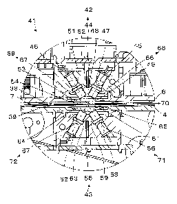
Banknote detecting unit 41 is located at banknote passageway 7 where a
banknote is
transported by banknote transporting unit 25.
Banknote detecting unit 41 of this present invention includes first emitting
sensor 68,
first reflecting sensor 69, second emitting sensor 71 and second reflecting
sensor 72.
These sensors are structured by upper sensor unit 42 which is fixed at upper
member 3 and
lower sensor unit 43 which is fixed at lower member 2.
CA 02454771 2004-01-05
12
Upper sensor unit 42 and iower sensor unit 43 are the same structure and are
located
symmetric to the up and down referring to banknote passageway 7.
Firstly upper sensor unit 42 is explained.
First emitting attaching hole 45 is formed at first sensor body 44, and the
axis line
crosses to banknote passageway 7 in an obtuse angle towards banknote entry B.
First receiving attaching hole 46 is formed upstream to hoie 45, and the axis
line crosses
to banknote passageway 7 at an acute angle.
First light emitting element 47 is fixed at the bottom (top) of first emitting
attaching
ho I e 45.
First light emitting element 47 is for example a red light emitting diode.
First emitting protecting cover 48 is fixed at the end of first emitting
attaching hole 45
and is made of a transparent resin: for example acrylate resin or glass and is
cylindrical,
In other words, first emitting section 49 is the end of first emitting
protecting cover 48.
After-mentioned protecting covers are made up as the same to first emitting
protecting
cover 48.
Second light receiving element 51 is fixed at the bottom (top) of first
receiving attaching
hole 46.
Second light receiving element 51 is for example iighttransistor.
Second receiving protecting cover 52 is fixed at the end of first receiving
attaching hole
46.
In other words, second light receiving section 53 is the end of second
receiving protecting
cover 52.
Second light receiving section 53 faces towards the rear to banknote entry 8,
therefore it
doesn't receive outside light.
First light emitting section 49 and second light receiving section 53 protrude
downwards
from the undersurface of first sensor body 44 and face to upper opening 54
which is formed
at upper banknote guiding surface 6.
When first light emitting section 49 and second light receiving section 53
protrude from
first sensor body 44, first light emitting section 49 and second light
receiving section 53
can be cleaned.
Therefore the adhered dust both on first light emitting section 49 and second
light
receiving section 53 are wiped away.
CA 02454771 2004-01-05
13
As a result, the sensor function is recovered easy,
Next lower sensor unit 43 is explained.
Second emitting attaching hole 56 is formed at second sensor body 55, and the
axis line
crosses to banknote passageway 7 in an obtuse angle towards banknote entry 8.
Second receiving attaching hole 57 is formed upstream at hole 56, and the axis
line crosses
at banknote passageway 7 in an acute angle.
Second light emitting element 58 is fixed at the bottom of second emitting
attaching hole
56,
Second light emitting element 58 is for example a red light emitting diode.
Second emitting protecting cover 59 is fixed at the end of second emitting
attaching hole
56.
In other words, second emitting section 61 is the end of second emitting
protecting cover
59.
First light receiving element 62 is fixed at the bottom of second receiving
attaching hole
57.
First light receiving element 62 is for exampie a lighttransistor,
First receiving protecting cover 63 is fixed at the end of second receiving
attaching hole
57.
In other words, first light receiving section 64 is the end of first receiving
protecting
cover 63.
First light receiving section 64 faces towards the rear to banknote entry 8,
therefore it
doesn't receive outside light.
Second light emitting section 61 and first light receiving section 64 protrude
upwards from
the upper surface of second sensor body 55 and faces to the lower opening 65
which is
formed at lower banknote guiding surface 4.
First light receiving section 64 is located on first light axis 66 of first
light emitting
section 49.
Second light receiving section 53 is located on second light axis 67 of second
emitting
section 61.
Therefore first light axis 66 and second light axis 67 crosses at transporting
line 70 of
banknote 9 at banknote passageway 7 at an obtuse angle, and it is X like in
shape.
CA 02454771 2004-01-05
14
By this, first light emitting section 49 and first light receiving section 64
structure
first light emitting sensor 68, and first light emitting section 49 and second
light
receiving section 53 structure first reflecting sensor 49.
Also, second light emitting section 61 and second light receiving section 53
structure
second emitting sensor 71, and second light emitting section 61 and first
light receiving
section 64 structure second reflecting sensor 72.
Next, banknote detecting circuit 73 is explained referring to figure 5.
Banknote detecting circuit 73 includes first switching circuit 75, second
switching circuit
78, first A/D converting circuit 77, second converting circuit 76 and reading
controlling
circuit 79.
First switching circuit 75 controls lighting of first Iight emitting element
47 based on
the direction of signals from microprocessor 74.
Second switching circuit 78 controls lighting of second iight emitting element
58 based on
the direction of signals from microprocessor 74.
First A/D converting circuit 77 converts from an analog signal of first light
receiving
element 62 to a digital signal, then the digital signal is outputted to
microprocessor 74.
Second A/D converting circuit 76 converts from an analog signal of second
light receiving
element 51 to a digital signal, then the digital signal is outputted to
microprocessor 74.
Reading controlling circuit 79 controls the outputting of first A/D converting
circuit 77
and second A/D converting circuit 76 to microprocessor 74.
Also, reading controlling circuit 79 can sample the output both of first A/D
converting
circuit 77 and second A/D converting circuit 76 based on the program of
microprocessor 74.
Microprocessor 74 outputs an authentic signal 80 to banknote 9 based on the
sampling data
from both of the first A/D converting circuit 77 and the second A/D converting
circuit 76.
Starting sensor 19 outputs the banknote signal to microprocessor 74.
Then microprocessor 74 controls the motor (not shown) of banknote transporting
unit 25
based on the banknote signal.
Next, the operation of the embodiment is explained referring to the tirning
chart in figure
6.
Banknote 9 1 s put on flat surface 14, then the left edge is moved along left
guiding board
CA 02454771 2004-01-05
5L.
When banknote 9 is a maximum width, the right edge is guided by right guiding
board 5R.
When the width of banknote 9 adapts to guiding rib 18, the right edge is
guided by guiding
rib 18.
The end of banknote 9 is guided by downward projection 13 and upward
projection 17, and
moves in zigzags, and comes to starting sensor 19.
The beam of starting emitting/receiving element 22 is cut off by banknote 9.
Accordingly, microprocessor 74 drives the motor (not shown), and banknote
transporting unit
10 25 starts.
Banknote 9 is moved more, and goes into the path between pulley 32 and beit
37.
Afterwards banknote 9 is transported by pulley 31 and belt 37 (in the right
direction in
figure 2).
In this process, banknote 9 is guided into the narrow path between the end of
upper
banknote stabilizer 38 and the end of lower banknote stabilizer 39.
If the banknote 9 has a crease, banknote 9 is stretched flat.
Accordingly, the distances between banknote 9 and first emitting sensor 68,
first
reflecting sensor 69, second emitting sensor 71, second reflecting sensor 72
become
2 0 approximately constant.
Afterwards banknote 9 is transported by pulley 32 and belt 37.
First switching circuit 75 and second switching circuit 78 are alternated "on"
and "off" by
microprocessor 74 until banknote 9 passed through from starting sensor 19 to
banknote
detecting unit 41.
In other words, first light emitting element 47 is turned on by electricity,
and emits
light at a predetermined time, afterwards second light emitting element 58 is
turned on by
electricity, and emits light at a predetermined time.
The processing is alternated to all length of banknote 9 at a short time.
In other words, the beam is emitted from first light emitting element 47, and
passes
through first emitting section 49, afterwards crosses banknote passageway 7,
then goes into
first light receiving section 64.
Afterwards, the beam is received into first light receiving element 62 and is
converted to
electrical signal P1 corresponding to the received light amount.
CA 02454771 2004-01-05
16
The receiving light amount is low level, because the beam passes through
bankriote 9.
At the same time, the emitted beam from first light emitting element 47 is
reflected by the
surface of banknote 9, afterwards it is received by second receiving section
53, then is
converted to electrical signal RI corresponding to the receiving light amount
by second
receiving element 51.
The received light amount of second receiving section 53 is higher than the
amount of first
receiving section 64, because it is based on the reflecting light.
When second light emitting element is turned on by electricity, it emits
light.
The beam is emitted from second light emitting element 58, and passes through
second
emitting section 61, afterwards crosses banknote passageway 7, then goes into
second light
receiving section 53.
Afterwards, the beam is received into second light receiving element 61 and is
converted to
electrical signal P2 corresponding to the received light amount.
At the same time, the emitted beam from second light emitting element 58 is
reflected by
the reverse of banknote 9, afterwards is received in first receiving section
64, then is
converted to electrical signal R2 corresponding to the receiving light amount
by first
receiving element 62.
2 0 Analog outputs P1 and P2 of first light receiving element 62 is converted
to digital
signals by first A/D converting circuit 77, and are outputted to
microprocessor 74.
Also, analog outputs R1 and R2 of second light receiving element 51 are
converted to
digital signals by second A/D converting circuit 76, and are outputted to
microprocessor 74.
Digital data which is based on the output of first light receiving element 62
outputs to
microprocessor 74 at timing signal T1 which is outputted by reading
controlling circuit 79
based on the signal of microprocessor 74, afterwards is sampled.
Next, at timing signal T2, the signal corresponding to signal R1 of first
reflecting sensor
69 is sampled as the same.
Also, at timing signal T3, the signal corresponding to signal P2 of second
emitting sensor
71 is sampled as the same.
Next, at timing signal T4, the signal corresponding to signal R2 of second
reflecting
sensor 72 is sampled as the same.
Above-mentioned sampling are executed at a predetermined times to all lengths
of banknote 9.
CA 02454771 2004-01-05
17
Afterwards, authenticity of the banknote 9 is distinguished based on the
sampling data in
microprocessor 74, and authenticity signal 80 is outputted.
As is clear from this embodiment, first emitting section 49 both of first
emitting sensor
68 and first reflecting sensor 49 and second emitting section 61 both of
second emitting
sensor 71 and second reflecting sensor 72 have a commonality.
When a pair of the emitting sensors and reflecting sensors are located, the
emitting
section and the receiving section are reduced by two from the prior art.
Therefore the instailation area is reduced and the price is reduced.
Also, when firstly the data either of first emitting sensor 68 or second
emitting sensor 71
is sampled, secondly the data either of first reflecting sensor 68 or second
reflecting
sensor 72, the lacework can be detected based on the data either of first
emitting sensor
68 or second emitting sensor 71, afterwards the data either of first
reflecting sensor 69
or second reflecting sensor 72 can be used -to distinguishing.
Therefore the distinguishing accuracy increases.
Next, the initial adjustment of banknote detecting unit 41 is explained
referring to figure
7.
The emitting amount of first light emitting element 47 is adjusted by first
light emitting
adjusting circuit 81 which is an emitting adjusting unit.
The output of first light emitting adjusting unit 81 is controlled by
microprocessor 74.
The output of second light receiving element 51 is adjusted by both amplifier
82 for the
second emitting sensor 71 and amplifier 83 for the first reflecting sensor 69.
The output of both the amplifier 82 for the second emitting sensor 71 and
amplifier 83 for
the first reflecting sensor 69 are converted from the analog signal to the
digital signal
by third A/D converting circuit 84, afterwards it is outputted to
microprocessor 74.
Amplifier 83 for first reflecting sensor 69 is a receiving outputting
adjusting unit.
The emitting amount of second light emitting element 58 is adjusted by second
light
3 0 emitting adjusting circuit 85 which is an emitting adjusting unit.
The output of second emitting adjusting circuit 85 is controlled by
microprocessor 74.
The output of f i rst I i ght rece i v i ng e i ement 62 is ad j usted by both
amp I i f i er 86 for the
first emitting sensor and amplifier 87 for the second reflecting sensor.
The output both of amplifier 86 for the first emitting sensor and amplifier 87
for the
second reflecting sensor are converted from the analog signal to the digital
signal by
CA 02454771 2004-01-05
18
third A/D converting circuit 84, afterwards it is outputted to microprocessor
74.
Amplifier 87 for second reflecting sensor is a receiving outputting adjusting
unit.
The initial setting is started by pushing the initial setting button 88.
Next the initial setting of banknote detecting unit 41 is explained referring
to figure 8,
The initial setting all of first emitting sensor 68, first reflecting sensor
69, second
emitting sensor 71 and second reflecting sensor 72 are the same,
Therefore the initial setting both of first emitting sensor 68 and first
reflecting sensor
69 are explained.
Firstly, initial setting button 88 is pushed, and initial setting signal IN is
sent to
microprocessor 74.
At step S1, when initial setting signal "IN" is distinguished, the program
goes to step S2.
At step S2, first light emitting element 47 emits at a predetermined voltage.
The output of first light receiving element 62 is amplified at a predetermined
gain by
amplifier 86 for first emitting sensor.
The amplified signal is converted to the digital signal by third A/D
converting circuit 84,
afterwards it is outputted to microprocessor 74.
At step S3, the output of amplifier 86 for first emitting sensor is compared
to a standard
vo I tage.
When the output does not corresponding to the standard voltage, the program
goes to step S4.
At step S4, when the output is larger than the standard voltage, the current
is adjusted to
reduce the light amount by first light amount adjusting circuit 81.
When the output is smaller than the standard voltage, the current is adjusted
to increase
the light amount by first light amount adjusting circuit 81.
By this adjustment, when the receiving light of first light receiving element
62 becomes at
a predetermined light amount, the program goes to step S5.
In other words, when the voltage of amplifier 86 becomes at a predetermined
voltage, the
program goes to step S5.
At step S5, a standard paper for adjusting is inserted into banknote
passageway from
banknote entry 8.
Also, the standard paper is transported by banknote transporting unit 25 as
the same as
banknote 9.
Afterwards, the standard paper is returned to the banknote entry. as the same
as a fake
CA 02454771 2004-01-05
19
banknote.
In this process, the output of second light receiving element 51 is amplified
by amplifier
83 for the first reflecting sensor, and is converted to a digital signal by
third A/D
converting circuit 84, afterwards is outputted to microprocessor 74.
At step S6, the digital signal is compared to the standard voltage.
When the digital signal does not correspond to the standard voltage, the
program goes to
step S7.
When the digital signal exceeds the standard voltage, the gain of amplifier 83
for first
reflecting sensor is reduced to correspond to the standard voltage.
By this, the initial setting finishes.
Also, the standard voltage can be set at a predetermined range.
The present invention can use a beam which is a first wave at the first
emitting section
and another beam which is a second wave at the second emitting section.
In this case, an emitting data, a reflecting data which is based on the first
wave and
another emitting data, another reflecting data which is based on the second
wave can get.
In other words, it can get four different data's in different situations.
Therefore the authenticity accuracy of the banknotes increases,
The number of the banknote detecting unit can be increased at width and length
of the
banknote.
As a result, the authenticity accuracy of the banknotes increases.
Also, the first emitting section can emit light which is an infrared rays, and
the second
emitting section can emit light which is non-infrared reys.
The cost of the infrared and the non-infrared light emitting element: for
example a red
light emitting diode are inexpensive.
Therefore the cost of the device is cheaper.
Also, only the first emitting sensor and the first reflecting sensor can be
used in the
banknote detecting unit.
In this case, only one of the light emitting element is reduced.
CA 02454771 2004-01-05
DESCRIPTION OF THE REFERENCE NUMERALS
7 banknote passageway
9 first light emitting section
13 second light receiving section
61 second light emitting section
64 first light receiving section
66 first light axis
67 second light axis
10 68 first emitting sensor
69 first reflecting sensor
79 reading controlling unit
81,85 emitting amount adjusting unit
83,87 receiving amount adjusting unit