Note: Descriptions are shown in the official language in which they were submitted.
CA 02455044 2004-O1-13
Strips for Analyzing Samples
BACKGROUND
A strip containing an electrochemical biosensor is useful to determine the
presence and
concentration of an analyte in a sample. Such a strip can be utilized, for
example, to monitor
glucose levels in diabetic patients.
SUMMARY
This invention features a strip for analyzing a sample, e.g., blood or urine.
The strip
includes two insulating layers, a spacer layer, and a conducting circuit.
The spacer layer is disposed between the two insulating layers, and configured
to define,
together with the two insulating layers, an adsorption port, a sample chamber,
a capillary for
delivering a sample from the adsorption port to the sample chamber through the
capillary, and a
vent for facilitating delivery of the sample into the sample chamber. An
adsorption port is an
inlet at an edge of the strip that tapers into a capillary. The spacer layer
can fi~rther define,
together with the two insulating layers, one or more additional adsorption
ports, sample
chambers, and capillaries.
~ s The conducting circuit is also disposed between the two insulating layers.
It includes a
working electrode, a counter electrode, conducting wires, and connectors. The
conducting
circuit can be printed on one or both insulating layers. For example, either
all elements of the
circuit are printed on one layer or some elements are printed on one layer and
the others on the
other layer. Both the working electrode and the counter electrode are in
association with a test
2o agent reactive to an analyte and at least a portion of each is placed in
the sample chamber. The
working electrode and the counter electrode are respectively connected to two
of the connectors
through the conducting wires. The connectors are adapted for electrical
connection to a meter
capable of measuring an electrical parameter. The test agent is an electron
transfer reagent that
transports electrons from the analyte to the working electrode. As a result,
an analyte-responsive
2s signal is generated and transmitted to the meter when a sample containing
the analyte enters the
sample chamber and contacts both the working electrode and the counter
electrode.
A strip of this invention can also include one or more other features. For
example, only
one of the two insulating layers has an indentation at the adsorption port so
that the adsorption
port is defined by the indentation, the other insulating layer, and the spacer
layer. Further, the
CA 02455044 2004-O1-13
sample chamber, but not the capillary, can be filled with a hydrophilic
material. Also, one or
more working and counter electrodes can be included in the strip. For example,
the strip can
include an additional working electrode, a portion of which is disposed in the
capillary, to
measure the conductivity of the sample in the capillary before it contacts a
hydrophilic material,
if any, in the sample chamber.
In one embodiment, the strip is a rectangle and has connectors at the rear
edge. It can
have an adsorption port disposed at the front edge or at one of the two side
edges, or two
adsorption ports disposed respectively at both side edges, or three adsorption
ports respectively
disposed respectively at the front edge and at both side edges.
In another embodiment, the strip is a pentagon in the shape of a rectangle
having a
clipped angle at the front edge, has an adsorption port disposed at the
slanting edge
corresponding to the clipped angle, and has connectors at the rear edge.
Optionally, it includes a
second adsorption port disposed at a side edge.
In still another embodiment, the strip is a hexagon in the shape of a
rectangle having two
~ s clipped angles at the front edge, has two adsorption ports respectively
disposed at the two
slanting edges corresponding to the two clipped angles, and has connectors at
the rear edge.
The strip can further include an indicator electrode, placed at the end of a
sample
chamber, to indicate that the sample chamber is filled with a sample. To
separate the counter
electrode from the working and indicator electrodes, the counter electrode can
be printed on one
2o insulating layer and the working and the indicator electrodes can be
printed on the other
insulating layer.
The strip can also include two capillaries bridging two adsorption ports to a
sample
chamber. It can further include an additional working electrode, two portions
of which are
placed in the two capillaries, respectively, to indicate the inception and the
completion of the
2s filling of the sample chamber with a sample.
The strip can further include two additional working electrodes, an indicator
electrode,
and a second sample chamber. A sample is delivered to the two sample chambers
via the same
capillary. At least a portion of the second working electrode is placed in the
capillary to measure
the conductivity of the sample. At least a portion of the third working
electrode, in association
so with another test agent, is placed in the second sample chamber to measure
the concentration of a
second analyte in the sample. A portion of the indicator electrode is placed
in the capillary to
CA 02455044 2004-O1-13
indicator the inception of the filling of the sample chamber. Two other
portions of the indicator
electrode are placed at the respective ends of the two sample chambers to
indicate that the
sample chambers are filled with the sample.
The details of one or more embodiments of the invention are set forth in the
accompa-
nying drawings and the description below. Other features, objects, and
advantages of the
invention will be apparent from the description and drawings, and from the
claims.
DESCRIPTION OF DRAWINGS
In the drawings, which are not to scale:
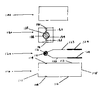
FIG 1 is an exploded view of a first embodiment of a strip of this invention
with a pair of
working and counter electrodes, all of which are printed on the same
insulating layer.
FIG 2 is an exploded view of a second embodiment of a strip of this invention
with two
working electrodes, a counter electrode, and an indicator electrode, all of
which are printed on
the same insulating layer.
FIG. 3 is an exploded view of a third embodiment of a strip of this invention
with two
~ s working electrodes and an indicator electrode, which are printed on an
insulating layer, and a
counter electrode, which is printed on another insulating layer.
FICA 4 is an exploded view of a fourth embodiment of a strip of this invention
having two
sample chambers. This strip includes three working electrodes and an indicator
electrode; which
are printed on a first insulating layer, and a counter electrode, which is
printed on a second
2o insulating layer.
Like reference symbols in the various drawings indicate like elements.
DETAILED DESCRIPTION
Four different embodiments of a strip of this invention are shown in FIGS. 1,
2, 3, and 4.
The four embodiments are to be construed as merely illustrative, and not
limitative of the
2s remainder of the disclosure in any way whatsoever. Without further
elaboration, it is believed
that one skilled in the art can, based on the description herein, utilize the
present invention to its
fullest extent.
The strip illustrated in FIG. 1 is a rectangle and includes insulating layer
110 and
insulating layer 140. Both insulating layers can be made of any suitable
insulating material such
so as a non-conducting polymer (e.g., polycarbonate, polyolefin, or
polyester), or an inorganic
CA 02455044 2004-O1-13
material (e.g., metal oxide). Insulating layer 110 further includes front edge
111, side edge 112,
side edge 113, rear edge 115 (also the rear edge of the strip), and
indentations 114.
Conducting circuit 120, shown in FIG. 1, is printed on insulating layer 110.
It includes
working electrode 121, counter electrode 122, conducting wires 123, and
connectors 124. The
term "working electrode" refers to an electrode on which an analyte is
electrooxidized or
electroreduced in the presence or absence of an electron transfer agent. The
term "counter
electrode" refers to an electrode paired with a working electrode, through
which passes an
electrochemical current equal in magnitude and opposite in sign to the current
passed through the
working electrode. An electrode can be made of an electrically conducting
material, such as
palladium, platinum, gold, silver, silver/silver chloride, and carbon. Both
working electrode 121
and counter electrode 122 respectively connect to two connectors 124 through
conducting wires
123. Connectors 124 are disposed at rear edge 115 and adapted for electrical
connection to a
meter (not shown) capable of measuring one or more electrical parameters, such
as current and
voltage. These two parameters can be detected by amperometry and
potentiometry, respectively.
~s Details of the detecting methods can be found, for example, in U.S. Patent
No. 6,299,757, which
is incorporated by reference in its entirety.
Overlaying working electrode 121 and counter electrode 122 is spacer layer
130, which is
disposed between insulating layer 110 and insulating layer 140. To facilitate
connection of
connectors 124 to a meter, insulating layer 140 is of such length that it does
not cover connectors
20 124. The spacer layer is typically constructed from a non-conductive
adhesive material, such as a
pressure-sensitive adhesive or a double-sided adhesive tape. Spacer layer 130,
together with
insulating layer 110 and insulating layer 140, defines two adsorption ports
131, one sample
chamber 133, and two capillaries 132 for delivering a sample from one of the
adsorption ports
131 to sample chamber 133 through the corresponding capillary 132. More
specifically, either
2s adsorption port 131 is defined by indentation 114, insulating layer 140,
and spacer layer 130.
The surface on insulating layer 140 facing indentation 114 provides a physical
baffle to a sample
and facilitates delivery of the sample to capillary 132. Without adsorption
port 131, rnass-
produced strips do not reproducibly draw a sample into capillary 132. When one
of the
adsorption ports 131 is used to draw a sample, the other adsorption port 131
functions as a vent
3o to facilitate delivery of the sample into sample chamber 133. The two
adsorption ports 131 are
disposed at side edge 112 and side edge 113, respectively. Sample chamber 133
exposes
4
CA 02455044 2004-O1-13
working electrode 121 and counter electrode 122, both of which are in
association with test agent
135. Details of the methods for providing a test agent in an electrochemical
biosensor strip can
be found, for example, in U.S. Patent No. 6,299,757. Whenever practical, a
test agent can be
provided in a sample. Unlike capillary 132, which is vacant, sample chamber
133 contains a
s hydrophilic material 134. The term "hydrophilic material" refers to a
material (in the form of
sheet, film, mesh, or granules) that wicks, filters, and retains a fluid
sample and does not prevent
diffusion of the sample to the electrodes. The hydrophilic material not only
facilitates the uptake
of a sample and retains it, but also reduces the required sample volume.
Suitable hydrophilic
materials include nylon, cellulose, polyvinyl alcohol, and
polyvinylpyrolidone. Hydrophilic
~ o material 134 is placed inside sample chamber 133 either before or after
test agent 135 has been
coated onto working electrode 121 and counter electrode 122. Hydrophilic
material 134 and test
agent 135 can also be mixed and placed inside sample chamber 133, resulting in
a coating on
working electrode 121 and counter electrode 122. Test agent 135 is an electron
transfer agent
that, upon reacting with an analyte, transports electrons between the analyte
in a sample and
working electrode 121. Such electron transfer can be realized either directly
via a one-
component test agent, such as ferricynide or ferrocence, or indirectly via a
two-component test
agent, such as a mixture of ferricynide and glucose oxidase or a mixture of
ferrocence and
glucose oxidase. Surfactant or plasma treatment of the walls of the adsorption
port, the capillary,
and the sample chamber can further facilitate the uptake of a sample.
2o When using a strip shown in FIG. 1, the end containing connectors 124 is
first plugged
into a meter. A sample flows into sample chamber 133, upon contacting
adsorption port 131,
and immerses both working electrode 121 and counter electrode 122 to form a
circuit. With a
potential applied between working electrode 121 and counter electrode 122, an
analyte-
responsive signal is generated and transmitted to the meter. The signal is
collected and the
2s concentration of the analyte is calculated and shown on the meter.
FIG. 2 illustrates another embodiment of a rectangular strip of this invention
with two
working electrodes 221 and 226, an indicator electrode 225, and a counter
electrode 222. The
term "indicator electrode" refers to an electrode that detects the inception
or the completion of
the filling of a sample chamber. This strip includes insulating layer 210 and
insulating layer 220.
so Insulating layer 210 further includes front edge 211, rear edge 213, and
indentation 212.
CA 02455044 2004-O1-13
Similar to that of the strip illustrated in FIG. l, conducting circuit 220 of
this strip is also
printed on insulating layer 210. It includes working electrode 221, working
electrode 226,
counter electrode 222, indicator electrode 225, conducting wires 223, and
connectors 224.
Conducting wires 223 are coated with a dielectric material (not shown) and
connectors 224 are
exposed. Unlike the strip shown in FIG. 1, this strip includes indicator
electrode 225 and
working electrode 226, both of which are respectively connected to two
connectors 224 through
conducting wires 223.
The strip illustrated in FIG. 2 contains spacer layer 230. Spacer layer 230,
together with
insulating layer 210 and insulating layer 240, defines adsorption port 231,
sample chamber 233,
vent 235, and capillary 232 for delivering a sample from adsorption port 231
to sample chamber
233 through capillary 232. Adsorption port 231 is an inlet to capillary 232
and vent 235 is an
opening of sample chamber 233 distal to adsorption port 231. Sample chamber
233 exposes
working electrode 221 and counter electrode 222, capillary 232 exposes working
electrode 226,
and vent 235 exposes indicator electrode 225. Hydrophilic material 234 is
placed inside sample
~ s chamber 233 and test agent 236 is coated on working electrode 221 and
counter electrode 222.
When a sample contacts both indicator electrode 225 and counter electrode 222,
a circuit
is formed and a signal is generated and transmitted to a meter to indicate
that the sample
chamber is filled with the sample. Another circuit is formed when a sample
contacts both
working electrode 226 in capillary 232 and counter electrode 222 in sample
chamber 233. With
2o a potential applied between working electrode 226 and counter electrode
222, a signal
corresponding to the conductivity of the sample is consequently generated and
transmitted to a
meter. When a sample enters sample chamber 233 and contacts both working
electrode 221 and
counter electrode 222, still another circuit is formed and a signal
corresponding to the
concentration of an analyte in the sample is generated and transmitted to the
meter with a
2s potential applied to these two electrodes.
FIG. 3 illustrates another embodiment of a rectangular strip of this invention
with counter
electrode 331 printed on one insulating layer 330, and two working electrodes
313 and 317 and
one indicator electrode 316 printed on the other insulating layer 310. This
strip includes
insulating layer 310, insulating layer 330, and a conducting circuit, which
consists of the above-
so mentioned electrodes, conducting wires 314, and connectors 315. Insulating
layer 310 further
includes front edge 311, indentation 312, rear edge 318, and hole 332.
6
CA 02455044 2004-O1-13
Part of the conducting circuit, including working electrode 3I3, working
electrode 317,
and indicator electrode 316 and their corresponding conducting wires 314 and
connectors 315, is
printed on insulating layer 310. The remainder of the conducting circuit,
including counter
electrode 331, is printed on insulating layer 330. Connectors 315 are exposed
at rear edge 318.
Spacer layer 320, together with insulating layer 310 and insulating layer 330,
defines
adsorption port 321, sample chamber 323, vent 325, and capillary 322 for
delivering a sample
from adsorption port 321 to sample chamber 323 through capillary 322.
Adsorption port 321 is
an inlet at front edge 311. Vent 325, an opening of sample chamber 323 distal
to adsorption port
321, is in communication with hole 332. Sample chamber 323 exposes working
electrode 313
~ o and a portion of counter electrode 331. Capillary 322 exposes working
electrode 317 and
another portion of counter electrode 331. Vent 325 exposes indicator electrode
316 and another
portion of counter electrode 331. Hydrophilic material 324 and test agent 326
are placed inside
sample chamber 323. By exposing a portion of counter electrode 331 and a
portion of working
electrode 317 in capillary 322, the conductivity of a sample can be accurately
measured without
~ s interference of hydrophilic material 324. Such interference normally
occurs when counter
electrode 331 is exposed in sample chamber 323, but not in capillary 322.
The strip illustrated in FIG.3 generates an electrochemical signal in a manner
similar to
that illustrated in FIG. 2. When a sample containing an analyte contacts
counter electrode 331 as
well as working electrode 313, working electrode 317, and indicator electrode
316, three circuits
2o are formed and signals are generated and transmitted to a meter showing the
concentration of the
analyte, the conductivity of the sample, and the completion of the filling of
sample chamber 323
with the sample, respectively.
Still another embodiment of a rectangular strip of this invention is
illustrated in FIG. 4. It
includes insulating layer 410, insulating layer 430, and a conducting circuit,
which consists of
25 the above-mentioned electrodes, conducting wires 414, and connectors 41 S.
Insulating layer 410
further includes front edge 411, rear edge 419, and indentation 412.
Part of the conducting circuit, including working electrode 413, working
electrode 417,
working electrode 418, and indicator electrode 416, and the corresponding
conducting wires 414
and connectors 415, is printed on insulating layer 410. The remainder of the
conducting circuit,
so including counter electrode 431, is printed on insulating layer 430.
Connectors 415, disposed at
rear edge 419, are exposed.
7
CA 02455044 2004-O1-13
Spacer layer 420, together with insulating layer 410 and insulating layer 430,
defines
adsorption port 421, sample chamber 423, sample chamber 424, two vents 426,
and capillary 422
for delivering a sample from adsorption port 421 to sample chamber 423 and
sample chamber
424 through capillary 422. Adsorption port 421 is disposed at front edge 411.
Vents 426 are,
respectively, openings of sample chamber 423 and sample chamber 424, both
distal to adsorption
port 421. Sample chamber 423 exposes working electrode 413 and a portion of
counter electrode
431. Sample chamber 424 exposes working electrode 418 and another portion of
counter
electrode 431. Capillary 422 exposes working electrode 417 and a third portion
of counter
electrode 431. A portion of indicator electrode 416 is positioned in capillary
422 in front of
working electrode 417. Two other portions of indicator electrode 416 are
positioned,
respectively, at an end of sample chamber 423 distal to adsorption port 421
and an end of sample
chamber 424 distal to adsorption port 421. Sample chamber 423 and sample
chamber 424 both
contain hydrophilic material 425. Test agent 427 and test agent 428, reagents
reactive to two
different analytes in a sample, are placed respectively inside sample chamber
423 and sample
~ 5 chamber 424.
When a sample containing two analytes enters capillary 422 and contacts both a
portion
of counter electrode 431 and a portion of the indicator electrode 416, a
circuit is formed and a
signal is generated and transmitted to a meter to indicate the inception of
the filling of the
sample. When the sample moves forward and contacts working electrode 417, a
potential being
2o applied between working electrode 417 and counter electrode 431, another
signal is generated
and transmitted to the meter to measure the conductivity of the sample. Two
other circuits are
formed when the sample contacts working electrode 413 and a portion of counter
electrode 431
in sample chamber 423, and contacts working electrode 418 and a portion of
counter electrode
431 in sample chamber 424, respectively. With a potential applied between
working electrode
2s 4I3 and counter electrode 431, an analyte-responsive signal is generated
and transmitted to the
meter to measure the concentration of the first analyte in the sample.
Similarly, with a potential
applied between working electrode 418 and counter electrode 431, another
analyte-responsive
signal is generated and transmitted to the meter to measure the concentration
of the second
analyte.
3o Note that the magnitude of a signal is generally proportional to the
surface area of an
electrode in contact with a sample. The contacting surface area of indicator
electrode 416
CA 02455044 2004-O1-13
increases by two folds when the sample reaches the two portions of indicator
electrode 416 at the
two vents 426 of sample chamber 423 and sample chamber 424. As a result, the
magnitude of
the signal passing through indicator electrode 416 also increases by two
folds, indicating that
sample chamber 423 and sample chamber 424 are filed with the sample.
OTHER EMBODIMENTS
All of the features disclosed in this specification may be combined in any
combination.
Each feature disclosed in this specification may be replaced by an alternative
feature serving the
same, equivalent, or similar purpose. Thus, unless expressly stated otherwise,
each feature
~ o disclosed is only an example of a generic series of equivalent or similar
features.
From the above description, one skilled in the art can easily ascertain the
essential
characteristics of the present invention, and without departing from the
spirit and scope thereof,
can make various changes and modifications of the invention to adapt it to
various usages and
conditions. Thus, other embodiments are also within the scope of the following
claims.
9