Note: Descriptions are shown in the official language in which they were submitted.
CA 02455694 2004-O1-23
Specification
Pressure Sensor
Background of the Invention
The present invention relates to a pressure
sensor in which a differential pressure sensor chip for
measuring a differential pressure and a static pressure
sensor chip for measuring a static pressure are stored
in one package.
Conventionally, as a method of measuring the
flow rate of a fluid, a method is available with which a
pressure difference between the upstream and downstream
of a restrictor is measured by utilizing the fact that
the pressure difference between the upstream and
downstream of the restrictor provided to a flow channel
is proportional to the flow velocity, and is converted
into a flow rate. With a liquid level indicator, the
pressure difference between the upper and lower portions
of a tank is measured, and a liquid level with a liquid
density being taken into consideration is measured from
the pressure difference. For such differential pressure
measurement, a differential pressure sensor is usually
used. The differential pressure sensor is a sensor that
receives two different to-be-measured pressures with
sensor chips simultaneously and-detects a differential
pressure between the two pressures.
Sometimes a static pressure, i.e., a gauge
- 1 -
CA 02455694 2004-O1-23
pressure with reference to an atmospheric pressure, or
an absolute pressure with reference to a vacuum state is
measured simultaneously with the differential pressure
described above, and monitoring and control are
performed simultaneously. As the differential pressure
sensor is a measurement unit that measures a pressure
difference between two points, it cannot measure the
static pressure itself.
A pressure sensor in which a differential
pressure measuring sensor chip and a static pressure
measuring sensor chip are combined is proposed as shown
in Japanese Patent Laid-Open No. 63-008524 (reference 1).
The pressure sensor disclosed in reference 1 is
constituted by a sensor housing incorporating a
differential pressure measuring sensor chip and static
pressure measuring sensor chip, and a main body which is
sealed with a pair of barrier diaphragms and into which
a sealed liquid has been injected. The sensor housing
and main body are fabricated separately, and are bonded
and fixed to each other.
In the conventional pressure sensor described
above, the interior of the main body is partitioned into
at least two inner chambers to correspond to the pair of
barrier diaphragms, and the sealed liquid is injected
into the respective inner chambers. A high
to-be-measured pressure applied to one barrier diaphragm
and a low to-be-measured pressure applied to the other
- 2 -
CA 02455694 2004-O1-23
barrier diaphragm are transmitted to the differential
pressure measuring sensor chip through the corresponding
sealed liquid. Either one of the high and low
to-be-measured pressures is transmitted to the static
pressure measuring sensor chip through the corresponding
sealed liquid. In this manner, as the conventional
pressure sensor has a complicated structure, its package
becomes undesirably large.
As the sensor housing and main body are
fabricated separately, the distances between the barrier
diaphragms and two sensor chips increase, and the
distance between the two sensor chips accordingly
increases. Therefore, in the conventional pressure
sensor, the amount of sealed liquid increases, and
accordingly the range of pressure that can be measured
becomes narrow, so that the temperature characteristics
are degraded.
To solve these problems, a differential
pressure sensor and static pressure sensor may be
integrally formed on one chip. To fabricate such a
pressure sensor, one semiconductor substrate is etched
to form a differential pressure measuring diaphragm and
static pressure measuring diaphragm at different regions.
Subsequently, strain gauges (in the case of
piezoelectric pressure sensors) or electrodes (in the
case of electrostatic capacitive pressure sensors) are
formed on the two diaphragms.
- 3 -
CA 02455694 2004-O1-23
When the differential pressure sensor and
static pressure sensor are integrally formed on one chip,
the manufacture becomes difficult and the cost increases.
More specifically, the differential pressure sensor and
static pressure sensor have different measurement ranges.
For this reason, the static pressure measuring diaphragm
must have a larger thickness and a smaller diameter than
those of the differential pressure measuring diaphragm,
so that it can withstand a large pressure.
When, however, the thickness of the diaphragm
of the differential pressure sensor and that of the
static pressure sensor are to be made different on one
semiconductor substrate, the manufacturing process will
become complicated. When the diameter of the diaphragm
decreases, the step of forming a strain gauge or
electrode on the diaphragm becomes difficult. When the
two diaphragms have the same thickness and the diameter
of the static pressure measuring diaphragm is increased,
the manufacturing process can be facilitated. In this
case, the sensitivity of the differential pressure
sensor may decrease unless the diameter of the
differential pressure measuring diaphragm is increased
as well. When the diameter of the differential pressure
measuring diaphragm is increased accordingly, the chip
size increases, and the cost increases.
It is an object of the present invention to
provide a pressure sensor that can obtain good
- 4 -
CA 02455694 2004-O1-23
temperature characteristics and a wide measurement
pressure range.
It is another object of the present invention
to provide a pressure sensor that can be manufactured
easily and allows a package to be downsized.
Summary of the Invention
A pressure sensor according to the present
invention comprises a differential pressure sensor chip
which has a differential pressure measuring diaphragm,
converts a pressure received by the differential
pressure measuring diaphragm into an electrical signal,
and outputs the electrical signal, a static pressure
sensor chip which has a static pressure measuring
diaphragm, converts a pressure received by the static
pressure measuring diaphragm into an electrical signal,
and outputs the electrical signal, a base on which the
differential pressure sensor chip and static pressure
sensor chip are mounted, the base having a first
pressure introducing channel for introducing a first
pressure to a first surface of the differential pressure
sensor chip, and a second pressure introducing channel
for introducing a second pressure to a first surface of
the static pressure sensor chip, and a pressure
introducing chamber which is formed in the base to
accommodate the differential pressure sensor chip and
static pressure sensor chip, and serves to introduce a
- 5 -
CA 02455694 2004-O1-23
third pressure commonly to a second surface of the
differential pressure sensor chip and a second surface
of the static pressure sensor chip.
Brief Description of Drawings
Fig. 1A is a sectional view of a pressure
sensor according to one embodiment of the present
invention, and Fig. 1B is a bottom view of the pressure
sensor shown in Fig. 1A; and
Fig. 2 is an enlarged sectional view of the
sensor chip shown in Figs. 1A and 1B.
Detailed Description of the Preferred Embodiment
The present invention will be described in
detail with reference to the drawings.
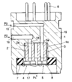
Figs. 1A and 1B show a pressure sensor
according to an embodiment of the present invention. As
shown in Fig. 1B, the pressure sensor of this embodiment
has a columnar header 1 serving as a base having a
stepped recess 1a, first and second prismatic first
pedestals 2 and 3 bonded and fixed to the bottom surface
of the recess la of the header 1 side by side, a
differential pressure measuring differential pressure
sensor chip 4 bonded and fixed on the first pedestal 2,
a static pressure measuring static pressure sensor chip
5 bonded and fixed on the second pedestal 3, a plurality
of sensor output pins 6 for guiding electrical signals
-6-
CA 02455694 2004-O1-23
from the sensor chips 9 and 5 to the outside, a circular
disk-like ceramic board 7 with a surface where wiring
patterns 9 (Fig. 1B) to electrically connect the sensor
chips 4 and 5 to the sensor output pins 6 are formed,
and a plurality of wires 8 for connecting the sensor
chips 4 and 5 and the sensor output pins 6 to each other
and the sensor chips 4 and 5 and the wiring patterns 9
to each other.
The sensor chips 4 and 5 bonded and fixed on
the pedestals 2 and 3 are respectively formed of known
piezoelectric pressure sensor chips. As shown in Fig. 2,
each of the piezoelectric pressure sensor chips 4 and 5
is constituted by a semiconductor diaphragm 41 and
strain gauges 42 formed on the semiconductor diaphragm
41 and having a piezoelectric resistor effect. In this
arrangement, the strain gauges 42 are deformed by the
pressure applied to the diaphragm 41. Changes in
resistance of the strain gauges 42 caused by the
piezoelectric resistor effect are detected, so that the
pressure is measured.
As the sensor chips 4 and 5, known
electrostatic capacitive pressure sensors may be used in
place of the piezoelectric pressure sensor chips. An
electrostatic capacitive pressure sensor chip has a
substrate with a predetermined space (capacitance
chamber), a diaphragm arranged on the space of the
substrate, a stationary electrode formed on the
CA 02455694 2004-O1-23
substrate, and a movable electrode formed on the
diaphragm. In this arrangement, upon reception of a
pressure, the diaphragm deforms, and the distance
between the movable and stationary electrodes changes
accordingly, so that the electrostatic capacitance
between the movable and stationary electrodes changes.
The pressure received by the diaphragm is measured on
the basis of the change in electrostatic capacitance.
According to another type of electrostatic
capacitive pressure sensor chip, a change in
electrostatic capacitance is detected not from
deformation of the diaphragm but from compression of the
material that forms the capacitance chamber. According
to still another type of pressure sensor chip, the
pressure is measured by modulating the displacement of
the diaphragm into an optical signal. When the
differential pressure sensor chip 4 and the static
pressure sensor chip 5 are compared, a smaller pressure
is applied to the diaphragm of the differential pressure
sensor chip 4. Thus, to improve the sensitivity, the
differential pressure sensor chip 4 has a larger
diaphragm diameter than that of the static pressure
sensor chip 5.
The sensor chips 4 and 5 having the above
structure are electrostatically bonded (anodic bonding)
to the end faces of the pedestals 2 and 3, respectively.
If thermal strain generated when bonding the sensor
_ g _
CA 02455694 2004-O1-23
chips 4 and 5 is transmitted to the sensor chips 4 and 5,
the temperature characteristics of the sensor chips 4
and 5 degrade to cause zero point shift. In view of
this, the pedestals 2 and 3 are made of a material
having a thermal expansion coefficient similar to that
of the sensor chips 4 and 5, e.g., a ceramic material
such as borosilicate glass (Corning 7740) or silicon
nitride.
The header 1 is made of a material having good
corrosion resistance and good weldability, e.g.,
stainless steel or Kovar. The pedestals 2 and 3, sensor
chips 4 and 5, ceramic board 7, and the like are
accommodated in the recess 1a formed at the center of
the lower surface of the header 1. Those end faces
(upper end faces) of the pedestals 2 and 3 which are
opposite to the sensor chips 4 and 5 are bonded and
fixed to the header 1 with a brazing material.
A through hole 7a through which the pedestals
2 and 3 are to extend is formed at the center of the
ceramic board 7. The through hole 7a has a shape of two
different-size, substantially square holes, when seen
from above, that are continuous to each other.
Insertion holes through which the sensor output pins 6
are to extend are formed in the peripheral portion of
the ceramic board 7 to surround the through hole 7a.
The wiring patterns 9 which electrically connect the
sensor chips 4 and 5 and the sensor output pins 6 to
- 9 -
CA 02455694 2004-O1-23
each other are formed on the surface of the ceramic
board 7 on the sensor chip side. The ceramic board 7 is
bonded to the header 1 at its peripheral portion with a
brazing material.
The terminals of the sensor chips 4 and 5 for
the power supply, ground, and detectors (strain gauges
in the case of piezoelectric pressure sensors, and
electrodes in the case of electrostatic capacitive
pressure sensors) and the wiring patterns 9 formed on
the ceramic board 7, and the sensor chips 4 and 5 and
the sensor output pins 6 are electrically connected to
each other through the wires 8 made of Au or the like.
The wiring patterns 9 and the sensor output pins 6 are
also electrically connected to each other through the
wires 8.
The sensor output pins 6 extending through the
header 1 and connected to the outside of the pressure
sensor are hermetically sealed with glass so that the
header 1 and the sensor output pins 6 are electrically
insulated from each other and that the sealed liquid is
prevented from leaking.
A circular pressure introducing chamber 17 for
introducing a to-be-measured pressure P1 commonly to the
lower surfaces of the sensor chips 4 and 5 is formed in
the lower opening side of the recess 1a of the header 1.
Pressure introducing channels 18 and 19 with L-shaped
sections for introducing to-be-measured pressures P2 and
- 10 -
CA 02455694 2004-O1-23
P3 on the outer surface of the header 1 to the bottom
surface of the recess 1a are formed in the header 1 such
that they open to the outer surface of the header 1 and
the bottom surface of the recess la, respectively. The
pedestal 2 has a hollow portion 2a which communicates
with the pressure introducing channel 18 of the header 1
and introduces the to-be-measured pressure P2 from the
pressure introducing channel 18 to the upper surface of
the differential pressure sensor chip 4. The pedestal 3
has a hollow portion 3a which communicates with the
pressure introducing channel 19 of the header 1 and
introduces the to-be-measured pressure P3 from the
pressure introducing channel 19 to the upper surface of
the static pressure sensor chip 5.
As the to-be-measured pressures P1, P2, and P3,
the pressure of a gas or liquid may be directly applied
to the sensor chips 9 and 5. Usually, barrier
diaphragms (not shown) which come into contact with a
to-be-measured fluid are arranged at measurement
positions formed by extending the pressure introducing
chamber 17 and pressure introducing channels 18 and 19.
A sealed liquid such as silicone oil is injected into
the pressure introducing chamber 17 and pressure
introducing channels 18 and 19 sealed by the respective
barrier diaphragms. Thus, the to-be-measured pressures
P1, P2, and P3 acting on the respective barrier
diaphragms are transmitted to the sensor chips 4 and 5
- 11 -
CA 02455694 2004-O1-23
through the sealed liquid.
The operation of the pressure sensor having
the above arrangement will be described. First, the
high to-be-measured pressure P1 is introduced to the
lower surface of the differential pressure sensor chip 4,
and the low to-be-measured pressure P2 is introduced to
the upper surface of the differential pressure sensor
chip 4. Thus, the differential pressure measuring
diaphragm of the differential pressure sensor chip 4
displaces in accordance with the differential pressure
(P1 - P2). At this time, the output voltage from the
differential pressure sensor chip 4 is extracted through
the sensor output pin 6, so that the differential
pressure (P1 - P2) is measured.
The to-be-measured pressure P1 is introduced
to the lower surface of the static pressure sensor chip
5, and the atmospheric pressure P3 is introduced to the
upper surface of the static pressure sensor chip 5.
Thus, the static pressure measuring diaphragm in the
static pressure sensor chip 5 displaces in accordance
with the differential pressure (P1 - P). At this time,
the output voltage from the static pressure sensor chip
5 is extracted through the sensor output pin 6, so that
the differential pressure (P1 - P3), i.e., the gauge
pressure, is measured. Also, the interior of the
pressure introducing channel 18 is set in a vacuum state,
so that the to-be-measured pressure Pl with reference to
- 12 -
CA 02455694 2004-O1-23
the vacuum state, i.e., the absolute pressure, is
measured.
In the pressure sensor according to this
embodiment, since gaps are present between the pedestals
2 and 3 and the ceramic board 7 and between the
pedestals 2 and 3, the sealed liquid enters the ceramic
board 7 and recess 1a as well, thus forming the pressure
introducing chamber 17. Usually, spacers are arranged
in the gaps between the pedestals 2 and 3 and the
ceramic board 7 and between the pedestals 2 and 3 so
that the amount of sealed liquid may be decreased. The
spacers are usually made of a ceramic material such as
alumina so that any change in volume caused by
temperature change may be prevented as much as possible.
As has been described above, according to the
present invention, the differential pressure sensor chip
and static pressure sensor chip are mounted on one base
so that their faces are exposed to the interior of the
common pressure introducing chamber. Thus, the
differential pressure sensor chip and static pressure
sensor chip can be arranged close to each other. The
amount of sealed liquid can be decreased to be smaller
than that in a conventional pressure sensor in which a
housing for the differential pressure sensor chip, a
housing for the static pressure sensor chip, and a main
body are fabricated separately and bonded to each other.
As a result, good temperature characteristics and a wide
- 13 -
CA 02455694 2004-O1-23
measurement pressure range can be obtained.
As the differential pressure sensor chip and
static pressure sensor chip can be arranged close to
each other, the structure of the pressure sensor is
accordingly simplified, so that the package can be
downsized. The manufacturing process for the pressure
sensor can be simplified, and the manufacturing cost can
be reduced. The differential pressure sensor chip and
static pressure sensor chip are fabricated in separate
manufacturing processes, and optimal diaphragms suited
to their applications can be formed in the respective
chips. When compared to a case wherein the differential
pressure sensor and static pressure sensor are
integrally formed on one chip, the manufacture becomes
easier, and the cost can be reduced more.
- 14 -