Note: Descriptions are shown in the official language in which they were submitted.
CA 02456383 2004-O1-28
MULTI-SEGMENTED PLANAR ANTENNA WITH BUILT-IN GROUND PLANE
BACKGROUND OF THE INVENTION
(1) FIELD OF THE INVENTION
This invention relates to a planar antenna having a built in ground
plane, a low profile, and small area which has excellent performance in close
proximity to either a conducting or non conducting surface.
(2) DESCRIPTION OF THE RELATED ART
A number of workers have disclosed planar type antennas.
U.S. Pat. No. 6,329,950 Bl describes a planar antenna having two
joined conducting regions connected to a coaxial cable.
U.S. Pat. No. 4,410,891 to Schaubert et al. describes a microstrip
antenna the polarization of which can easily be changed.
U.S. Pat. No. 6,097,345 to Walton describes a dual band slot antenna
for cellular telephone and global positioning system frequency bands.
U.S. Pat. No. 6,429,828 B1 to Tinaphong et al. describes a VHF/L1HF
self tuning planar antenna system.
SUMMARY OF THE INVENTION
Antennas are essential in any electronic systems containing wireless
links. Such applications as communications and navigation require reliable
sensitive
1
CA 02456383 2004-O1-28
antennas. It is very desirable if these antennas are compact, stable, and are
not
affected by the proximity of either conductive or non conductive surfaces.
In is a principle objective of this invention to provide a very low
profile, small area antenna that has excellent performance in close proximity
to either
conducting or non conductive surfaces.
In is another principle objective of this invention to provide a method
of forming very low profile, small area antenna that has excellent performance
in
close proximity to either conducting or non conductive surfaces.
These objectives are achieved using a mufti-segmented planar antenna
with a built in ground plane. The antenna elements are formed on a layer of
first
dielectric having conducting material on both the first and second sides of
the layer of
first dielectric, such as a printed circuit board. First and second antenna
elements are
formed on the first side of the layer of first dielectric using selective
etching of the
conducting material on the first side of the layer of dielectric. Third and
fourth
antenna elements are formed on the second side of the layer .of first
dielectric using
selective etching of the conducting material on the second side of the layer
of
dielectric.
The first and second antenna elements are generally rectangular
separated by a narrow gap and electrically connected by two shorting strips
across the
gap. The third and fourth antenna elements are long and nan-ow wherein the
length of
the third antenna element is an integral multiple of a quarter 'wavelength of
a first
frequency and the length of the fourth antenna element is an integral multiple
of a
quarter wavelength of a second frequency. The first and second frequencies are
the
operating frequencies of the antenna. The widths of the segments of the third
antenna
element are not the same. The widths of the segments of the fourth antenna
element
are not the same. Conducting vias connect the first antenna element with the
first end
of the and third antenna element and the second antenna element with the first
end of
the fourth antenna element. A small shorting strip electrically connects the
second
end of the third antenna element to the second end of the fouk~th antenna
element.
2
CA 02456383 2004-O1-28
A layer of second dielectric is placed between the layer of first
dielectric having the first, second, third, and fourth antenna elements and a
ground
plane. A cavity is formed in the layer of second dielectric for a coaxial
cable. The
center conductor of the coaxial cable is connected to the second end of the
third
antenna element. The shield of the coaxial cable is connected to the ground
plane,
Two conducting pins connect the second antenna element to the ground plane.
The
antenna element can be fully encapsulated in a plastic encapsulation material
having
an exit port for the coaxial cable, thereby protecting the antenna assembly
from the
effects of the environment.
BRIEF DESCRIPTION OF THE DRAV~INGS
Fig. 1 shows a cross section view of the circuit board on which the
antenna elements are to be formed.
Fig. 2A shows the top view of the first and second antenna elements.
Fig. 2B shows the bottom view of the third and fourth antenna
elements.
Fig. 3A shows a cross section view of a part of the circuit board on
which the antenna elements are formed showing the conducting path between the
first
and third antenna elements.
Fig. 3B shows a cross section view of a part of the circuit board on
which the antenna elements are formed showing the conducting path between the
second and fourth antenna elements.
Fig. 4 shows a top view of the layer of dielectric placed between the
circuit board on which the antenna elements are formed and the ground plane.
Fig. 5 shows a top view of the ground plane showing the connection
between a coaxial cable shield and the ground plane.
3
CA 02456383 2004-O1-28
Fig. 6 shows a top view of the completed antenna.
Fig. 7 shows a cross section view of the completed antenna showing
the connection of the center conductor of a coaxial cable to the third antenna
element.
Fig. 8 shows a cross section view of the completed antenna showing
the conducting paths between the second antenna element and the ground plane.
Fig. 9 shows a cross section view of the completed antenna which has
been encapsulated in plastic.
Fig. 10 shows a flow diagram of the method of this invention.
DESCRIPTION OF THE PREFERRED EMBODIMENTS
Refer now to Figs. 1-9 for a description of thf; preferred embodiment of
the antenna of this invention. Fig. 1 shows a cross section view of a layer of
first
dielectric material 34 having a top surface 23 and a bottom surface 25. A
first layer of
conducting material 15 is formed on the top surface 23 of the layer of first
dielectric
material 34 and a second layer of conducting material 17 is formed on the
bottom
surface 25 of the layer of first dielectric material 34. As an example the
first 15 and
second 17 layers of conducting material can be a metal such as copper and
formed on
the layer of first dielectric material 34 by means of deposition, lamination,
plating, or
the like, This layer of dielectric with conducting material on the top and
bottom is
used to form the antenna elements of this antenna.
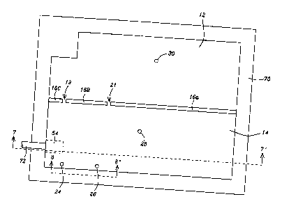
Fig. 2A shows a top view of the layer of dielectric material with
conducting layers on both the top and the bottom showing a :first antenna
element 12
and a second antenna element 14 formed in the first layer of conducting
material
using a means such as selective etching. The layer of dielectric material with
conductive layers on both the top and the bottom has a rectangular shape with
a first
length 112 and a first width 110. A notch 10 is removed from the layer of
dielectric
material with conductive layers on both the top and the bottom to accommodate
and
additional antenna if one is desired. The notch has a second length 116 and a
second
4
CA 02456383 2004-O1-28
width 114. The first antenna element 12 is separated from the second antenna
element 14 by a gap having a first segment 16A, a second segment 168, and a
third
segment 16C each segment having a third width 22. A first shorting strip 19
separates
the second segment 16B of the gap from the third segment 16C of the gap and
electrically connects the first antenna element 12 to the second antenna
element 14. A
second shorting strip 21 separates the first segment 16A of the gap from the
second
segment 16B of the gap and electrically connects the first antenna element 12
to the
second antenna element 14. The first shorting strip 19 and t:he second
shorting strip
21 have the same width, a fourth width 18. The antennas' resonance frequencies
and
resonance impedances can be fine tuned by the location of the first 19 and
second 21
shorting strips. of the antenna There is a conducting path 30 between the
first
antenna element 12 and a third antenna element and a conducting path 28
between the
second antenna element 14 and a fourth antenna element. 'there are conducting
paths, 24 and 26, between the second antenna element 14 and a ground plane.
The
third anc fourth antenna elements and the ground plane are yet to be
described.
Fig. 2B shows a bottom view of the layer of dielectric material with
conducting layers on both the top and the bottom showing a third antenna
element;
36A, 368, and 36C; and a fourth antenna element;38A, 38B, 38C, and 38D; formed
in
the second layer of conducting material using a means such as selective
etching. The
third antenna element has a first segment 36A having a fifth width 42 and a
third
length 118, a second segment 36B having a sixth width 44 a~ad a fourth length
120,
and a third segment 36C having the sixth width 44 and a ftfth length 122. The
fourth
antenna element has a first segment 38A having the sixth width 44 and a sixth
length
124, a second segment 38B having the sixth width 44 and a seventh length 126,
a
third segment 38C having the sixth width 44 and an eighth lEngth 128, and a
fourth
segment 38B having the sixth width 44 and a ninth length 130. The sum of the
third
118, fourth 120 and fifth 122 lengths is equal to an integral multiple of one
quarter of
the wavelength of a first frequency. The sum of the sixth 124, seventh 126,
eighth
128, and ninth 130 lengths is equal to an integral multiple of one quarter of
the
wavelength of a second frequency.
The fifth 42 and sixth 44 widths are chosen to achieve the desired
impedance of the third and fourth antenna elements. A third shorting strip 40
having
5
CA 02456383 2004-O1-28
a tenth width 52 electrically connects one end of the first segment 36A of the
third
antenna clement with one end of the fourth segment 38I7 of the fourth antenna
element. As shown in Figs. 2B and 3A the conducting path 30 between the third
antenna element and the first antenna element is located at the free end of
the third
segment 36C of the third antenna element and goes directly through the layer
of first
dielectric 34. As shown in Figs. 2B and 3B the conducting ;path 28 between the
fourth
antenna element and the second antenna element is located at the free end of
the first
segment 38A of the fourth antenna element and goes directly through the layer
of first
dielectric 34. As an example these conducting paths, 28 and 30, can be plated
through
holes, filled holes, or like. One end of the first segment 36P, of the first
antenna
element has a contact point 50 for connection to the center conductor of a
coaxial
cable.
As an example the first frequency is between about 148 and 151 MHz
and the second frequency is between about 136 and 140 MH:z. The dimensions of
the
antenna are scaled to correspond to the desired frequencies a.nd examples of
some of
the dimensions of the antenna will be given to correspond to the example
frequencies.
Those skilled in the art will readily recognize that the antenna dimensions
can be
scaled to operate at other frequencies. In this example the first length 112
is about
10.25 inches and the first width 110 is about 7.25 inches. The second length
116 and
the second width 114 are both between about 1.0 and 1.375 inches. The third
width
22 is about 1/32 inches and the fourth width 18 is between about 0.05 and 0.25
inches,
see Fig. 2A.
In this example the third length 1 I8 is about J.125 inches, the fourth
length 120 is about 5 .3125 inches, and the fifth length 122 i s about 4.1875
inches
which is consistent with the first frequency. of between about 148 and 151
MHz. In
this example the sixth length 12.4 is about 3.635, the seventh length 126 is
about
3.4375 inches, the eighth length 128 is about 8.0 inches, and the ninth length
130 is
about 4.0 i aches which is consistent with the second frequency of between
about I36
and 140 .NIHz. As previously indicated the dimensions can be scaled to achieve
an
antenna having good operating characteristics at different frequencies.
6
CA 02456383 2004-O1-28
Fig. 4 shows a top view of a layer of second dielectric 56 which will be
placed between the layer of first dielectric having the first, second, third,
and fourth
antenna elements formed thereon and a ground plane. The layer of second
dielectric
56 has a first cavity 54 formed therein to enable a coaxial cable to make
connections
to the contact point 50 on the first segment 36A of the third antenna element
as well
as to the ground plane. The layer of second dielectric 56 can also have a
second
cavity 58 formed therein to accommodate an edge connector, not shown. Fig. 5
shows a top view of a ground plane 70 of the antenna of this invention. The
ground
plane is a conducting material such as copper. The ground plane 70 has a
contact
region 78 to connect to the shield 74 of a coaxial cable 72. 'the center
conductor 76
of the coaxial cable 72 is to be connected to the third antenna element. The
ground
plane 70 also has connection points, 25 and 27, to connect to the conducting
paths, 24
and 26 shown in Fig. 2A, between the second antenna element and the ground
plane.
Fig. 6 shows a top view of the completed antenna assembly. Fig. 7
shows a cross section view of the completed antenna assembly taken along line
7-T of
Fig. 6. Fig. 7 shows the connection of the center conductor 76 of the coaxial
cable 72
to the connection region 50 on the first segment 36A of the third antenna
element and
the connection of the shield 74 of the coaxial cable 72 to the connection
region 78 on
the ground plane 70. Fig. 8 shows a cross section view of a part of the
completed
antenna assembly taken along line 8-8' of Fig. 6. Fig. 8 shows the conduction
paths,
24 and 2G, between the second antenna element 14 and the ground plane 70. As
shown in Fig. 8 all of the conducting material has been removed from this
region of
the second surface of the layer of first dielectric 34.
As shown in Fig. 9, the antenna assembly can be fully encapsulated in
a plastic material 80 or other suitable insulating and encapsulating material.
'The cross
section of the antenna assembly shown in Fig. 9 is also taken along line 7-T
of Fig. 6.
As shown in Fig. 9, the plastic encapsulating material 80 covers the ground
plane 70,
the top of the antenna assembly, and the edges of the antenna assembly. The
coaxial
cable 72 extends through the plastic encapsulating material 80.
The antenna described herein can be scaled to operate efficiently at
frequeoc:.s between about 3 KHz to 300 GHz.
7
CA 02456383 2004-O1-28
Fig. 10 shows a flow diagram of the method of forming an antenna of
this invention. As shown in the first box 140, a layer of first dielectric
material
having a top surface, a bottom surface, a first layer of conducting material
on the top
surface of the layer of first dielectric material, and a second layer of
conducting
material formed on the bottom surface of the layer of first dielectric
material is
provided. As shown in the next hox 142, the antenna elements and shorting
strips are
formed in the first and second layers of conducting material. As shown in the
next
box 144, conducting paths are formed between the first and third antenna
elements
and between the second and fourth antenna elements. As shown in the next box
146,
a layer of second dielectric having a cavity for a coaxial cable formed
therein is
provided. As shown in the next box 148 a ground plane is provided. As shown in
the
next box 150, the assembly is formed by placing the layer of. second
dielectric on the
ground plane and the layer of first dielectric with the antenna elements
formed thereon
is placed on the layer of first dielectric. As shown in the next box 152
conduction
paths are formed between the ground plane and the second antenna element. As
shoran in the next box 154, the coaxial cable is connected to the antenna
assembly.
As shown in the next box 156 the assembly is encapsulated if desired. The
steps
shown in Fig. 10 have been previously described in greater detail.
While the invention has been particularly shown and described with
reference to the preferred embodiments thereof, it will be understood by those
skilled
in the art that various changes in form and details may be made without
departing
from the spirit and scope of the invention.