Note: Descriptions are shown in the official language in which they were submitted.
CA 02456937 2004-02-04
90141 US
ANTENNA ELEMENT, FEED PROBE; DIELECTRIC SPACER, ANTENNA AND
METHOD OF COMMUNICATING WITH A PLURALITY OF DEVICES
CROSS-REFERENCE TO RELATED APPLICATIONS
This application claims the benefit of priority from provisional patent
application Serial No:
60/482,689, filed June 26, 2003, entitled Antenna Element, Multiband Antenna,
And
Method Of Communicating With A Plurality Of Devices. Provisional patent
application
Serial No. 60/482,689, is incorporated herein by reference in its entirety
FIELD OF THE INVENTION
The present invention relates in its various aspects to an antenna element; a
proximity-
coupling feed probe for an antenna; a dielectric spacer for an antenna; an
antenna (which
may be single band or multiband), and a method of communicating with a
plurality of
devices. The invention is preferably but not exclusively employed in a base
station
antenna for communicating with a plurality of terrestrial mobile devices.
BACKGROUND OF THE INVENTION
In some wireless communication systems, single band array antennas are
employed.
However in many modern wireless communication systems network operators wish
to
provide services under existing mobile communication systems as well as
emerging
systems. In Europe GSM and DCS1800 systems currently coexist and there is a
desire to
operate emerging third generation systems (UMTS) in parallel with these
systems. In
North America network operators wish to operate AMPSINADC, PCS and third
generation
systems in parallel.
As these systems operate within different frequency bands separate radiating
elements
are required for each band. To provide dedicated antennas for each system
would
require an unacceptably large number of antennas at each site. It is thus
desirable to
provide a compact antenna within a single structure capable of servicing all
required
frequency bands.
CA 02456937 2004-02-04
Base station antennas for cellular communication systems generally employ
array
antennas to allow control of the radiation pattern, particularly down tilt.
Due to the narrow
band nature of arrays it is desirable to provide an individual array for each
frequency
range. When antenna arrays are superposed in a single antenna structure the
radiating
elements must be arranged within the physical geometrical limitations of each
array whilst
minimising undesirable electrical interactions between the radiating elements.
US 200310052825 A1 describes a dual band antenna in which an annular ring
radiates an
omni-directional "doughnut" pattern for terrestrial communication capability,
and an inner
circular patch generates a single lobe directed towards the zenith at a
desired SATCOM
frequency.
WO 99/59223 describes a dual-band microstrip array with a line of three low
frequency
patches superposed with high frequency crossed dipoles. Additional high
frequency
crossed dipoles are also mounted between the low frequency patches. Parasitic
sheets
are mounted below the crossed dipoles.
Guo Yong-Xin, Luk Kwai-Man, Lee Kai-Fong, "L-Probe Proximity-Fed Annular Ring
Microstrip Antennas'; IEEE Transactions on Antennas and Propagation, Vol. 49,
No. 1, pp
19-21, January 2001 describes a single band, single polarized antenna. The L-
probe
extends past the centre of the ring, so cannot be combined with other L-probes
for a dual-
polarized feed arrangement.
EXEMPLARY EMBODIMENT
A first aspect of an exemplary embodiment provides a multiband base station
antenna for
communicating with a plurality of terrestrial mobile devices, the antenna
including one or
more modules, each module including a low frequency ring element; and a high
frequency
element superposed with the low frequency ring element.
The high frequency element can be located in the aperture of the ring without
causing
shadowing problems. Furthermore, parasitic coupling between the elements can
be used
to control the high andlor low frequency beamwidth.
Preferably the low frequency ring element has a minimum auter diameter b, a
maximum
inner diameter a, and the ratio bla is less than 1.5. A relatively low b/a
ratio maximizes
2
CA 02456937 2004-02-04
the space available in the center of the ring for locating the high band
element, for a given
outer diameter.
The antenna may be single polarized, or preferably dual polarized.
Typically the high frequency element and the low frequency ring element are
superposed
substantially concentrically, although non-concentric configurations may be
possible.
Typically the high frequency element has an outer periphery, and the low
frequency ring
element has an inner periphery which completely encloses the outer periphery
of the high
frequency element, when viewed in plan perpendicular to the antenna. This
minimizes
shadowing effects.
The antenna can be used in a method of communicating with a plurality of
terrestrial
mobile devices, the method including communicating with a first set of said
devices in a
low frequency band using a ring element; and communicating with a second set
of said
devices in a high frequency band using a high frequency element superposed
with the
ring element.
The communication may be one-way, or preferably a two-way communication.
Typically the ring element communicates via a first beam with a first half-
power
beamwidth, and the high frequency element communicates via a second beam with
a
second half-power beamwidth which is no more than 50% different to the first
beamwidth.
This can be contrasted with US 2003/0052825 A1 in which the beamwidths are
substantially different.
A further aspect of an exemplary embodiment provides a multiband antenna
including one
or more modules, each module including a low frequency ring element; and a
dipole
element superposed with the low frequency ring element. The antenna can be
used in a
method of communicating with a plurality of devices, the method including
communicating
with a first set of said devices in a low frequency band using a ring element;
and
communicating with a second set of said devices in a high frequency band using
a dipole
element superposed with the ring element.
CA 02456937 2004-02-04
We have found that a dipole element is particularly suited to being used in
combination
with a ring. The dipole element has a relatively low area (as viewed in plan
perpendicular
to the ring), and extends out of the plane of the ring, both of which may
reduce coupling
between the elements.
A further aspect of an exemplary embodiment provides an antenna element
including a
ring, and one or more feed probes extending from the ring, wherein the ring
and feed
probes) are formed from a unitary piece.
Forming as a unitary piece enables the ring and feed probes) to be
manufactured easily
and cheaply. Typically each feed probe meets the ring at a periphery of the
ring. This
permits the probe and ring to be easily formed from a unitary piece.
A further aspect of an exemplary embodiment provides an antenna element
including a
ring; and a feed probe having a coupling section positioned proximate to the
ring to enable
the feed probe to electromagnetically couple with the ring, wherein the
coupling section of
the feed probe has an inner side which cannot be seen within an inner
periphery of the
ring when viewed in plan perpendicular to the ring.
This aspect provides a compact arrangement, which is particularly suited for
use in a dual
polarized antenna, and/or in conjunction with a high frequency element
superposed with
the ring within its inner periphery. An electromagnetically coupled probe is
preferred over
a conventional direct coupled probe because the degree of proximity between
the probe
and the ring can be adjusted, to tune the antenna.
Typically the element further includes a second ring positioned adjacent to
the first ring to
enable the second ring to electromagnetically couple with said first ring.
This improves
the bandwidth of the antenna element.
A further aspect of an exemplary embodiment provides a dual polarized antenna
element
including a ring; and two or more feed probes, each feed probe having a
coupling section
positioned proximate to the ring to enable the feed probe to
electromagnetically couple
with the ring.
A further aspect of an exemplary embodiment provides an antenna feed probe
including a
feed section; and a coupling section attached to the feed section, the
coupling section
4
CA 02456937 2004-02-04
having first and second opposite sides, a distal end remote from the feed
section; and a
coupling surface which is positioned, when in use, proximate to an antenna
element to
enable the feed probe to efectromagnetically couple with an antenna element,
wherein the
first side of the coupling section appears convex when viewed perpendicular to
the
coupling surface, and wherein the second side of the coupling section appears
convex
when viewed perpendicular to the coupling surface.
A probe of this type is particularly suited for use in conjunction with a ring
element, the
'concavo-convex' geometry of the element enabling the element to align with
the ring
without protruding beyond the inner or outer periphery of the ring. In one
example the
coupling section is curved. In another, the coupling section is V-shaped.
A further aspect of an exemplary embodiment provides a multiband antenna
including an
array of two or more modules, each module including a low frequency ring
element and a
high frequency element superposed with the low frequency ring element.
The compact nature of the ring element enables the centres of the modules to
be closely
spaced, whilst maintaining sufficient space between the modules. This enables
additional
elements, such as interstitial high frequency elements, to be located between
each pair of
adjacent modules in the array. A parasitic ring may be superposed with each
interstitial
high frequency element. The parasitic rings) present a similar environment to
the high
band elements which can improve isolation as well as allowing the same
impedance
tuning for each high frequency element.
A further aspect of an exemplary embodiment provides a multiband antenna
including one
or more modules, each module including a low frequency ring element; and a
high
frequency element superposed with the low frequency ring element, wherein the
low
frequency ring element has a non-circular inner periphery.
The non-circular inner periphery can be shaped to ensure that sufficient
clearance is
available for the high frequency element, without causing shadowing effects.
This
enables the inner periphery of the ring to have a minimum diameter which is
less than the
maximum diameter of the high frequency element.
A further aspect of an exemplary embodiment provides a microstrip antenna
including a
ground plane; a radiating element spaced from the ground plane by an air gap;
a feed
CA 02456937 2004-02-04
probe having a coupling section positioned proximate to the ring to enable the
feed probe
to electromagnetically couple with the ring; and a dielectric spacer
positioned between the
radiating element and the feed probe.
This aspect can be contrasted with conventional proximity-fed microstrip
antennas, in
which the radiating element and feed probe are provided on opposite sides of a
substrate.
The size of the spacer can be varied easily; to control the degree of coupling
between the
probe and radiating element.
A further aspect of an exemplary embodiment provides a dielectric spacer
including a
spacer portion configured to maintain a minimum spacing between a feed probe
and a
radiating element; and a support portion configured to connect the radiating
element to a
ground plane, wherein the support portion and spacer portion are formed as a
unitary
piece.
Forming the spacer portion and support portion from a single piece enables the
spacer to
be manufactured easily and cheaply.
BRIEF DESCRIPTION OF THE DRAWINGS
The accompanying drawings which are incorporated in and constitute part of the
specification, illustrate embodiments of the invention and, together with the
general
description of the invention given above, and the detailed description of the
embodiments
given below, serve to explain the principles of the invention.
Figure shows a perspective view of a single antenna
1 module;
Figure shows a cross section through part of the
1 a PCB;
Figure shows a plan view of a Microstrip Annular
2a Ring (MAR);
Figure shows a perspective view of the MAR;
2b
Figure shows a side view of the MAR;
2c
Figure shows a perspective view of a Crossed Dipole
3a Element (CDE);
Figure shows a front view of a first dipole part;
3b
Figure shows a rear view of the first dipole part
3c
Figure shows a front view of a second dipole part;
3d
Figure shows a rear view of the second dipole part
3e
Figure shows a perspective view of a dual module;
4
CA 02456937 2004-02-04
Figure 5 shows a perspective view of an antenna array;
Figure 6a shows a plan view of an antenna array with parasitic rings;
Figure 6b shows a perspective view of the array of Figure 6a;
Figure 7a shows a plan view of a parasitic ring;
Figure 7b shows a side view of the parasitic ring;
Figure 7c shows an end view of the parasitic ring
Figure 7d shows a perspective view of the parasitic ring
Figure 8 shows a perspective view of an antenna employing a single piece
radiating
element;
Figure 9A shows an end view of an alternative probe;
Figure 9B shows a side view of the probe;
Figure 9C shows a plan view of the probe;
Figure 10 shows a plan view of a square MAR;
Figure 11 shows an antenna array incorporating square MARs;
Figure 12 shows an isometric view of an antenna;
Figure 13 shows a plan view of one end of the antenna;
Figure 14 shows an end view of a clip;
Figure 15 shows a side view of the clip;
Figure 16 shows a plan view of the clip;
Figure 17 shows a first isometric view of the clip;
Figure 18 shows a second isometric view of the clip;
Figure 19 shows a side view of an MAR;
Figure 20 shows a top isometric view of the MAR;
Figure 21 shows a bottom isometric view of the MAR;
Figure 22 shows a single band antenna; and
Figure 23 shows a dual-band antenna communicating with a number of land-based
mobile devices.
DETAILED DESCRIPTION OF EMBODIMENTS OF THE INVENTION
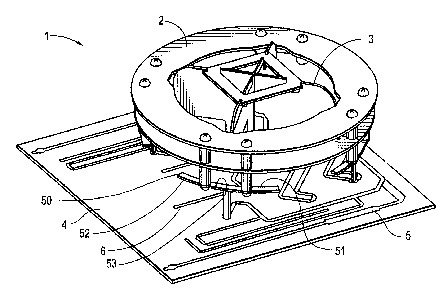
Figure 1 shows a single antenna module 1, comprising a single low frequency
Microstrip
Annular Ring (MAR) 2 and a single high frequency Crossed Dipole Element (CDE)
3
centred in the MAR 2. The MAR 2 and CDE 3 are mounted on a printed circuit
board
(PCB). The PCB comprises a substrate 4 which carries a microstrip feedline
network 5
coupled to the MAR 2, and a microstrip feedline network 6 coupled to the CDE
3. As
shown in Figure 1 a (which is a cross section through part of the PCB), the
other face of
CA 02456937 2004-02-04
the substrate 4 carries a ground plane 7. The MAR 2 and CDE 3 are shown
separately in
Figures 2a-c and Figures 3a-f respectively.
Referring to Figures 2a-c, the MAR 2 comprises an upper ring 10, lower ring
11, and four
T-probes 12a,12b. Each T-probe 12a,12b is formed from a single T-shaped piece
of
metal with a leg 13 and a pair of arms 15. The leg 13 is bent down by 90
degrees and is
formed with a stub 14 which passes through a hole in the PCB and is soldered
to the feed
network 5. Thus the leg 13 and stub 14 together form a feed section, and the
arms 15
together form a coupling section. Referring to Figure 1, the arms 15 each have
a distal.
end 50 remote from the feed section, an inner side 51 and an outer side 52,
and an upper
surface 53 which couples capacitively with the lower ring 11. The arms 15
extend
circumferentially with respect to the ring, and have the same centre of
curvature as the
outer periphery of the lower ring 11. Therefore the outer sides 52 appear
convex when
viewed perpendicular to the upper surface 52, and the inner sides 51 appears
convex
when viewed perpendicular to the upper surface 52.
The arms 15 of the T-probe couple capacitively with the tower ring 11, which
couples
capacitively in turn with the upper ring 10. The rings 10,11 and the T-probes
12a,12b are
separated by plastic spacers 16 which pass through apertures in the arms 15 of
the T-
probe and the lower ring 11. The spacers 16 are received in the apertures as a
snap fit,
and have a similar construction to the arms 122 described below with reference
to Figure
17.
The T-probes 12a are driven out of phase provide a balanced feed across the
ring in a
first polarization direction, and the T-probes 12b are driven out of phase to
provide a
balanced feed across the ring in a second polarization direction orthogonal to
the first
direction.
An advantage of using electromagneticaily (or proximity) coupled feed probes
(as
opposed to direct coupled feed probes which make a direct conductive
connection) is that
the degree of coupling between the lower ring 11 and the T-probes can be
adjusted for
tuning purposes. This degree of coupling may be adjusted by varying the
distance
between the elements (by adjusting the length of the spacers 16), and/or by
varying the
area of the arms 15 of the T-probe.
CA 02456937 2004-02-04
It can be seen from Figures 1 and 2c that air gaps are present between the
upper ring 10,
the lower ring 11, the arms 15 of the T-probes and the PCB. In a first
alternative
proximity-coupling arrangement (not shown), the MAR may be constructed without
air
gaps, by providing a single ring as a coating on an outer face of a two-layer
substrate. A
proximity coupled microstrip stub feedline is provided between the two
substrate layers,
and a ground plane on the opposite outer face of the two-layer substrate.
However the
preferred embodiment shown in Figures 1 and 2a-2c has a number of advantages
over
this alternative embodiment. Firstly, there is an ability to increase the
distance between
the arms 15 of the T-probe and the lower ring 11. 1n the alternative
embodiment this can
only be achieved by increasing the substrate thickness, which cannot be
increased
indefinitely. Secondly, the rings 10 and 11 can be stamped from metal sheets,
which is a
cheap manufacturing method. Thirdly, because the legs 13 of the T-probes are
directed
away from the ground plane 7, the distance between the ground plane and the
rings 10,
11 can easily be varied by adjusting the length of the legs 13. It has been
found that the
bandwidth of the antenna can be improved by increasing this distance.
fn a second alternative proximity-coupled arrangement (not shown); the MAR may
have a
single ring 11, or a pair of stacked rings 10, 11, and the T-probes may be
replaced by L-
probes. The L-probes have a leg similar to the leg 13 of the T-probe, but only
a single
coupling arm which extends radially towards the centre of the ring. The second
alternative embodiment shares the same three advantages as the first
alternative
embodiment. However, the use of radially extending L-probes makes it difficult
to arrange
a number of L-probes around the ring for a dual-polarized feed; due to
interference
between inner edges of the coupling arms. The inner parts of the L-probes
would also
reduce the volume available for the CDEs 3.
Note that the concave inner sides 51 of the arms of the T-probes cannot be
seen within
the inner periphery of the ring when viewed in plan perpendicular to the ring,
as shown in
Figure 2a. This leaves this central volume (that is, the volume of projection
of the inner
periphery of the ring, projected onto the ground plane) free to accommodate
the CDE. It
also ensures that the T-probes are spaced apart to minimize interference.
The "concavo-convex" shape of the arms 15 of the T-probes conforms to the
shape of the
lower ring, thus maximising the coupling area whilst leaving the central
volume free.
9
CA 02456937 2004-02-04
The upper ring 10 has a larger outer diameter than the lower ring 11 (although
in an
alternative embodiment it could be smaller). However the inner diameter, and
shape, of
each of the rings, is the same. Specifically, the inner periphery of the rings
is circular with
four notches 19 formed at 90 degree intervals. Each notch has a pair of
straight angled
sidewalls 17 and a base 18. As can be seen in the Figure 1, and the plan view
of Figure
6a, the diameter of the CDE 3 is greater than the minimum inner diameter of
the rings.
The provision of notches 19 enables the inner diameter of the rings to be
minimised,
whilst providing sufficient clearance for the arms of the CDE 3. Minimising
the inner
diameter of the rings provides improved performance, particularly at high
frequencies.
The lower ring 11 has a minimum outer diameter b, a maximum inner diameter a,
and the
ratio b/a is approximately 1.36. The upper ring 12 has a minimum outer
diameter b', a
maximum inner diameter a', and the ratio b'/a' is approximately 1.40. The
ratios may vary
but are typically lower than 10, preferably less than 2.0, and most preferably
less than 1.5.
A relatively low bla ratio maximizes the central volume available for locating
the CDE.
Referring to Figures 3a-e, the CDE 3 is formed in three parts: namely a first
dipole part 20,
a second dipole part 21, and a plastic alignment clip 22. The first dipole
part comprises
an insulating PCB 23 formed with a downwardly extending slot 24. The front of
the PCB
23 carries a stub feedline 25 and the back of the PCB 23 carries a dipole
radiating
element comprising a pair of dipole legs 26 and arms 27. The second dipole
part 21 is
similar in structure to the first dipole part 20, but has an upwardly
extending slot 28. The
CDE 3 is assembled by slotting together the dipole parts 20, 21, and mounting
the clip 22
to ensure the dipole parts remain locked at right-angles.
The PCB 23 has a pair of stubs 29 which are inserted into slots (not shown) in
the PCB 4.
The feedline 25 has a pad 30 formed at one end which is soldered to the
microstrip
feedline network 6.
The small footprint of the MAR 2 prevents shadowing of the CDE 3. By centring
the CDE
3 in the MAR 2, a symmetrical environment is provided which leads to good port-
to-port
isolation for the high band. The MAR is driven in a balanced manner, giving
good port-to-
port isolation for the low band.
A dual antenna module 35 is shown in Figure 4. The dual module 35 includes a
module 1
as shown in Figure 1. An additional high frequency CDE 36 is mounted next to
the
CA 02456937 2004-02-04
module 1. The microstrip feedline network 6 is extended as shown to feed the
CDE 36.
The CDE 36 may be identical to the CDE 3. Alternatively, adjustments to the
resonant
dimensions of the CDE 36 may be made for tuning purposes (for instance
adjustments to
the dipole arm length, height etc).
An antenna for use as part of a mobile wireless communications network in the
interior of
a building may employ only a single module as shown in Figure 1, or a dual
module as
shown in Figure 4. However, in most external base station applications, an
array of the
form shown in Figure 5 is preferred. The array of Figure 5 comprises a line of
five dual
modules 35, each module 35 being identical to the module shown in Figure 4.
The PCB is
omitted in Figure 5 for clarity. The feedlines are similar to feedlines 5, 6,
but are extended
to drive the modules together.
Different array lengths can be considered based on required antenna gain
specifications.
The spacing between the CDEs is half the spacing between the MARs, in order to
maintain array uniformity and to avoid grating lobes.
The modules 35 are mounted, when in use, in a vertical line. The azimuth half-
power
beamwidth of the CDEs would be 70-90 degrees without the MARs. The MARs narrow
the azimuthal half-power beamwidth of the CDEs to 50-70 degrees.
An alternative antenna array is shown in Figures 6a and 6b. The array is
identical to the
array shown in Figure 5, except that additional parasitic rings 40 have been
added. One
of the parasitic rings 40 is shown in detail in Figures 7a-d. The ring 40 is
formed from a
single piece of stamped sheet metal, and comprises a circular ring 41 with
four legs 42. A
recess (not labelled) is farmed in the inner periphery of the ring where the
ring meets each
leg 42. This enables the legs 42 to be easily bent downwardly by 90 degrees
into the
configuration shown. The legs 42 are formed with stubs (not labelled) at their
distal end,
which are received in holes (not shown) in the PCB. In contrast to the legs 13
of the T-
probes, the legs 42 of the parasitic rings 40 are not soldered to the feed
network 5,
although they may be soldered to the ground plane 7. Hence the rings 40 act as
"parasitic" elements. The provision of the parasitic rings 40 means that the
environment
surrounding the CDEs 36 is identical, or at least similar, to the environment
surrounding
the CDEs 3. The outer diameter of the parasitic rings 40 is smaller than the
outer
diameter of the MARs in order to fit the parasitic rings into the available
space. However,
the inner diameters can be similar, to provide a consistent electromagnetic
environment.
n
CA 02456937 2004-02-04
An alternative antenna is shown in Figure 8. The antenna includes a singe
piece radiating
ring 45 (identical in construction to the parasitic ring 40 shown in Figure 7a-
7d). The legs
46 of the ring are coupled to a feed network 47 on a PCB 48. In contrast to
the rings 40 in
Figure 6a and 6b (which act as parasitic elements), the ring 45 shown in
Figure 8 is
coupled directly to the feed network and thus acts as a radiating element.
An air gap is provided between the ring 45 and the PCB 48. In an alternative
embodiment
(not shown), the air gap may be filled with dielectric material.
An alternative electromagnetic probe 60 is shown in Figures 9A-9C. The probe
60 can be
used as a replacement to the T-probes shown in Figures 1 and 2. The probe 60
has a
feed section formed by a leg 61 with a stub 62, and an arm 63 bent at 90
degrees fio the
leg 61. Extending from the arm 63 are six curved coupling arms, each arm
having a distal
end 64, a concave inner side 65, a convex outer side 56, and a planar upper
coupling
surface 67. Although six coupling arms are shown in Figures 9A-9C, in an
alternative
embodiment only four arms may be provided. In this case, the probe would
appear H-
shaped in the equivalent view to Figure 9C.
An alternative antenna module 70 is shown in Figure 10. In contrast to the
circular MAR
of Figure 1; the module 70 has a square MAR 71 with a square inner periphery
72 and a
square outer periphery 73. The T-probes shown in the embodiment of Figures 1
and 2
are replaced by T-probes formed with a feed leg (not shown) and a pair of arms
74
extending from the end of the feed teg. The arms 74 are straight, and together
form a V-
shape with a concave outer side 75 and a convex inner side 76. A CDE 76
(identical to
the CDE 3 of Figure 1) is superposed concentrically with the ring 61, and its
arms extend
into the diagonal corners of the square inner periphery 72.
An antenna formed from an array of modules 70 is shown in Figure 11.
Interstitial high
band CDEs 77 are provided between the modules 70. Although only three modules
are
shown in Figure 11, any alternative number of modules may be used (for
instance five
modules as in Figure 5).
An alternative multiband antenna 100 is shown in Figures 12 and 13. In common
with the
antenna of Figure 5, the antenna 100 provides broadband operation with low
12
CA 02456937 2004-02-04
intermodulation and the radiating elements have a relatively small footprint.
The antenna
100 can be manufactured at relatively low cost.
A sheet aluminium tray provides a planar reflector 101, and a pair of angled
side walls
102. The reflector 101 carries five dual band modules 103 on its front face,
and a PCB
104 on its rear face (not shown). The PCB is attached to the rear face of the
reflector 101
by plastic rivets (not shown) which pass through holes 105 in the reflector
101. Optionally
the PCB may also be secured to the reflector with double sided tape. The front
face of the
PCB, which is in contact with the rear face of the reflector 101, carries a
continuous
copper ground plane layer. The rear face of the PCB carries a feed network
(not shown).
Coaxial feed cables (not shown) pass through cable holes 111,112 in the side
walls 102
and cable holes 113 in the reflector 101. The outer conductor of the coaxial
cable is
soldered to the PCB copper ground plane layer. The central conductor passes
through a
feed hole 114 in the PCB through to its rear side, where it is soldered to a
feed trace. For
illustrative purposes, one of the feed traces 110 of the 'feed network can be
seen in Figure
13. Note however that in practice the feed trace 110 would not be visible in
the plan view
of Figure 13 (since it is positioned on the opposite face of the PCB).
Phase shifters (not shown) are mounted on a phase shifter tray 115. The tray
115 has a
side wall running along the length of each side of the tray. The side walls
are folded into a
C shape and screwed to the reflector 101.
In contrast to the arrangement of Figures 1, 4 and 8 (in which-the feed
network faces the
radiating elements, with no intervening shield), the reflector 101 and PCB
copper ground
plane provide a shield which reduces undesirable coupling between the feed
network and
the radiating elements.
Each dual band module 103 is similar to the module 35 shown in Figure 4, so
only the
differences will be described below.
The annular rings and T-probe of the MAR are spaced apart and mounted to the
reflector
by four dielectric clips 120, one of the clips 120 being shown in detail in
Figures 14-18.
Referring first to the perspective view of Figure 17, the clip 120 has a pair
of support legs
121, a pair of spacer arms 122, and an L-shaped body portion 123. Referring to
Figure
13
CA 02456937 2004-02-04
15, the end of each support leg 121 carries a pair of spring clips 123, each
spring clip
having a shoulder 124. Each spacer arm 122 has a pair of lower, central and
upper
grooves 128, 129, and 130 respectively. A pair of lower, central and upper
frustoconical
ramps 125, 126 and 127 are positioned next to each pair of grooves. Each arm
also has
a pair of openings 131,132 which enable the ramps 128-130 to flex inwardly. A
pair of
leaf springs 133 extend downwardly between the legs 121. The clip 120 is
formed as a
single piece of injection moulded DeIrinT"' acetal resin. The body portion 123
is formed
with an opening 134 to reduce wall thickness. This assists the injection
moulding process.
Each module 103 includes an MAR shown in detail in Figures 19-21. Note that
for clarity
the CDE is omitted from Figures 19-21. The MAR is assembled as follows.
Each T-probe is connected to a respective clip by passing the spacer arms
through a pair
of holes (not shown) in the T-probe. The lower ramps 125 of the spacer arms
122 flex
inwardly and snap back to hold the T-probe securely in the lower groove 128
The MAR includes a lower ring 140 and upper ring 141. Each ring has eight
holes (not
shown). The holes in the lower ring 140 are larger than the holes in the upper
ring 141.
This enables the upper ramps 127 of the spacer arm to pass easily through the
hole in the
lower ring. As the lower ring 140 is pushed down onto the spacer arm, the
sides of the
hole engage the central ramps 126 which flex inwardly, then snap back to hold
the ring
securely in the central grooves 129. The upper ring 141 can then be pushed
down in a
similar manner into upper grooves 130, past ramp 127 which snaps back to hold
the
upper ring securely in place
After assembly, the MAR is mounted to the panel by snap fitting the support
legs 121 of
each clip into holes (not shown) in the reflector 101, and soldering the T-
probes 143 to the
feed network. When the spring clips 123 snap back into place, the reflector
101 is held
between the shoulder 124 of the spring clip and the bottom face of the leg
121. Any slack
is taken up by the action of the leaf springs 133, which apply a tension force
to the
reflector 101, pressing the shoulder 124 against the reflector.
The clips 120 are easy to manufacture, being formed as a single piece. The
precise
spacing between the grooves 128-130 enables the distance between the elements
to be
controlled accurately. The support legs 121 and body portion 123 provide a
relatively rigid
14
CA 02456937 2004-02-04
support structure for the elements, and divert vibrational energy away from
the solder joint
between the T-probe and the PCB.
A further alternative antenna is shown in Figure 22. The antenna of Figure 22
is identical
to the antenna of Figure 12, except that the antenna is a single band antenna,
having only
MAR radiating elements (and no high frequency CDEs). Certain features of the
dual band
antenna shown in Figure 22 (for instance the shaped inner periphery of the
MARs, the
holes in the reflector for the CDEs) are unnecessary in a single band antenna,
so may be
omitted in practice.
A typical field of use of the multiband antennas described above is shown in
Figure 23. A
base station 90 includes a mast 91 and multiband antenna 92. The antenna 92
transmits
downlink signals 93 and receives uplink signals 94 in a tow frequency band
to/from
terrestrial mobile devices 95 operating in the low band. The antenna 92 also
transmits
downlink signals 96 and receives uplink signals 97 in a low frequency band
to/from mobile
devices 98 operating in the high band. The downtilt of the high band and low
band beams
can be varied independently.
In a preferred example the low band radiators are sufficiently broadband to be
able to
operate in any wavelength band between 806 and 960 MHz. For instance the low
band
may be 806-869 MHz, 825-894 MHz or 870-960 MHz. Similarly, the high band
radiators
are sufficiently broadband to be able to operate in any wavelength band
between 1710
and 2170 MHz. For instance the high band may be 1710-1880 MHz, 1850-1990 MHz
or
1920-2170 MHz. However it will be appreciated that other frequency bands may
be
employed, depending on the intended application.
The relatively compact nature of the MARs, which are operated in their lowest
resonant
mode (TM~~), enables the MARs to be spaced relatively closely together,
compared with
conventional low band radiator elements. This improves performance of the
antenna,
particularly when the ratio of the wavelengths for the high and low band
elements is
relatively high. For instance, the antenna of Figure 12 is able to operate
with a frequency
ratio greater than 2.1:1. The CDEs and MARs have a spacing ratio of 2:1. In
wavelength
terms, the CDEs are spaced apart by 0.82J~ and the MARs are spaced apart by
0.75A, at
the mid-frequency of each band. Thus the ratio between the mid-frequencies is
2.187:1.
At the high point of the frequency band, the CDEs are spaced apart by 0.92A
and the
is
CA 02456937 2004-02-04
MARs are spaced apart by 0.81A (the ratio between the high-point frequencies
being
2.272:1 ).
While the present invention has been illustrated by the description of the
embodiments
thereof, and while the embodiments have been described in detail, it is not
the intention of
the Applicant to restrict or in any way limit the scope of the appended claims
to such
detail.
For example, the CDEs may be replaced by a patch element, or a "travelling-
wave"
element.
The MARs, parasitic rings 40 or single piece radiating rings 45 may be square,
diamond
or elliptical rings (or any other desired ring geometry), instead of circular
rings. Preferably
the rings are formed from a continuous loop of conductive material (which may
or may not
be manufactured as a single piece).
Although the radiating elements shown are dual-polarized elements, single-
polarized
elements may be used as an alternative. Thus for instance the MARs, or single
piece
radiating rings 45 may be driven by only a single pair of probes on opposite
sides of the
ring, as opposed to the dual-polarized configurations shown in Figures 1 and
12 which
employ four probes.
Furthermore, although a balanced feed arrangement is shown, the elements may
be
driven in an unbalanced mariner. Thus for instance each polarization of the
MARs or the
single piece rings 45 may be driven by only a single probe, instead of a pair
of probes on
opposite sides of the ring.
Additional advantages and modifications will readily appear to those skilled
in the art.
Therefore, the invention in its broader aspects is not limited to the specific
details,
representative apparatus and method, and illustrative examples shown and
described.
Accordingly, departures may be made from such details without departure from
the spirit
or scope of the Applicant's general inventive concept.
l6