Note: Descriptions are shown in the official language in which they were submitted.
CA 02457325 2004-02-09
WO 03/014774 PCT/US02/25228
1
AMPLIFIED TREE STRUCTURE TECHNOLOGY
FOR FIBER OPTIC SENSOR ARRAYS
Background of the Invention
Field of the Invention
[0001] The present invention is in the field of fiber optic acoustic sensor
arrays
wherein light is propagated in the arrays and the effects of acoustic signals
on the light
returning from the arrays are analyzed to determine the characteristics of the
acoustic
signals.
Description of the Related Art
[0002] Fiber optic based acoustic sensors are promising alternatives to
conventional electronic sensors. Included among their advantages are a high
sensitivity, large dynamic range, light weight, and compact size. The ability
to easily
multiplex a large number of fiber optic sensors onto common busses also makes
fiber
optic sensors attractive for large-scale arrays. The recent successful
incorporation of
multiple small-gain erbium doped fiber amplifiers (EDFAs) into a fiber optic
sensor
array to increase the number of sensors that can be supported by a single
fiber pair has
made large-scale fiber optic sensor arrays even more competitive.
[0003] For acoustic detection, the fiber optic sensor of choice has been the
Mach-
Zehnder interferometric sensor. In any interferometric sensor, phase
modulation is
mapped into an intensity modulation through a raised cosine function. Because
of this
nonlinear transfer function, a sinusoidal phase modulation will generate
higher order
harmonics. An interferometer biased at quadrature (interfering beams 7/2 out
of
phase) has a maximized response at the first order harmonic and a minimized
response
at the second order harmonic. For this reason, quadrature is the preferred
bias point.
As the bias point drifts away from quadrature (for example, due to external
temperature changes), the response at the first order harmonic decreases and
the
response at the second order harmonic increases. When the interferometer is
biased at
0 or 7t out of phase, the first order harmonic disappears completely. This
decreased
CA 02457325 2004-02-09
WO 03/014774 PCT/US02/25228
2
response at the first order harmonic (resulting from the bias points away from
quadrature) is referred to as signal fading.
[0004] Because Mach-Zehnder interferometric sensors have an unstable bias
point, they are especially susceptible to the signal fading problem just
mentioned. In
order to overcome signal fading, a demodulation of the returned signal is
required.
The typical demodulation technique is the Phase-Generated Carrier (PGC)
scheme,
which requires a path-mismatched Mach-Zehnder interferometric sensor. (See,
for
example, Anthony Dandridge, et al., Multiplexing of Interferometric Sensors
Using
Phase Carrier Techniques, Journal of Lightwave Technology, Vol. LT-5, No. 7,
July
1987, pp. 947-952.) This path imbalance also causes the conversion of laser
phase
noise to intensity noise, which limits the performance of the Mach-Zehnder
interferometric sensor arrays at low frequencies and places stringent
requirements on
the linewidth of the source. This narrow linewidth requirement has slowed the
development of amplified Mach-Zehnder interferometric sensor arrays at 1.55
m.
[0005] The Sagnac interferometer has found widespread use in the fiber optic
gyroscopes. (See, for example, B. Culshaw, et al., Fibre optic gyroscopes,
Journal of
Physics E (Scientific Instruments), Vol. 16, No. 1, 1983, pp. 5-15.) It has
been
proposed that the Sagnac interferometer could be used to detect acoustic
waves. (See,
for example, E. Udd, Fiber-optic acoustic sensor based on the Sagnac
interferometer,
Proceedings of the SPIE-The International Society for Optical En ing eering,
Vol. 425,
1983, pp. 90-91; Kjell Krakenes, et al., Sagnac interferometer for underwater
sound
detection: noise properties, OPTICS LETTERS, Vol. 14, No. 20, October 15,
1989,
pp. 1152-1145; and Sverre Knudsen, et al., An Ultrasonic Fiber-Optic
Hydrophone
Incorporating a Push-Pull Transducer in a Sagnac Interferometer, JOURNAL OF
LIGHTWAVE TECHNOLOGY, Vol. 12, No. 9, September 1994, pp. 1696-1700.)
Because of its common-path design, the Sagnac interferometer is reciprocal and
therefore has a stable bias point, which eliminates signal fading and prevents
the
conversion of source phase noise into intensity noise. Therefore, the Sagnac
interferometer is immune to the phase noise which limits the Mach-Zehnder
interferometric sensors at low frequencies.
CA 02457325 2004-02-09
WO 03/014774 PCT/US02/25228
3
Summary of the Invention
[0006] One aspect of the present invention is a sensor array that comprises a
source of light and a first coupler that receives the light from the source.
The first
coupler couples a first portion of the light to a first coupler port and
couples a second
portion of the light to a second coupler port. An interferometric loop has a
first end
coupled to the first coupler port to receive the first portion of the light
and has a
second end coupled to the second coupler port to receive the second portion of
the
light. The interferometric loop propagates the first portion of the light in a
first
direction to the second coupler port and propagates the second portion of the
light in a
second direction opposite the first direction to the first coupler port. The
interferometric loop comprises a plurality of sensors coupled in parallel
between the
first end of the interferometric loop and the second end of the
interferometric loop.
The sensors perturb light passing through the sensors in response to a sensed
parameter (e.g., acoustic signals). A first plurality of couplers distribute
the first
portion of the light approximately equally to each of the sensors, collect the
second
portion of the light from each of the sensors, and propagate the collected
light to the
first end of the interferometric loop. A second plurality of couplers
distribute the
second portion of the light approximately equally to each of the sensors,
collect the
first portion of the light from each of the sensors, and propagate the
collected light to
the second end of the interferometric loop. At least one first amplifier is
coupled
between the first end of the interferometric loop and the first plurality of
couplers. At
least one second amplifier is coupled between the second end of the
interferometric
loop and the second plurality of couplers. A plurality of delay portions are
connected
between the first and second ends of the interferometric loops and the
sensors. The
delay portions have delays selected so that the light passing through each
sensor is
delayed by a different amount than the light passing through the other
sensors.
Preferably, the first plurality of couplers further comprise a first
distribution coupler
that receives the first portion of the light from the first amplifier and
distributes the
first portion of the light to a first plurality of internal amplifiers that
are coupled
between the first distribution coupler and a first plurality of internal
couplers. The
CA 02457325 2004-02-09
WO 03/014774 PCT/US02/25228
4
first distribution coupler collects the second portion of the light from the
first plurality
of internal amplifiers and propagates the second portion of the light to the
first
amplifier. Also preferably, the second plurality of couplers further comprise
a second
distribution coupler that receives the second portion of the light from the
second
amplifier and distributes the second portion of the light to a second
plurality of
internal amplifiers that are coupled between the second distribution coupler
and a
second plurality of internal couplers. The second distribution coupler
collects the first
portion of the light from the second plurality of internal amplifiers and
propagates the
first portion of the light to the second amplifier. The first plurality of
internal
couplers distribute the first portion of the light to the plurality of sensors
and collect
the second portion of the light from the plurality of sensors. The second
plurality of
internal couplers distribute the second portion of the light to the plurality
of sensors
and collect the first portion of the light from the plurality of sensors.
Advantageously,
the source of light is a broadband source, such as, for example, a
superfluorescent
fiber source. Also advantageously, the first and second amplifiers and the
first and
second plurality of internal amplifiers are erbium-doped fiber amplifiers, and
the first
and second distribution couplers and the first and second pluralities of
internal
couplers comprise 4 x 4 couplers.
[00071 Another aspect of the present invention is a method of sensing a
parameter
that comprises propagating light from a source of light through an
interferometric loop
such that approximately equal portions of the light counterpropagate in first
and
second directions in the loop. The light propagating in the first direction of
the
interferometric loop is amplified and coupled into a plurality of sensors such
that
approximately equal portions of the light propagating in the first direction
are passed
through each of the sensors. The light propagating in the second direction of
the
interferometric loop is amplified and coupled into the plurality of sensors
such that
approximately equal portions of the light propagating in the second direction
are
passed through each of the sensors. The light propagating in the first
direction is
caused to interfere with the light propagating in the second direction to
generate a
plurality of output signals responsive to light passing through each sensor in
the first
CA 02457325 2004-02-09
WO 03/014774 PCT/US02/25228
and second directions. Each of the sensors perturbs light passing therethrough
in
response to a sensed parameter (e.g., an acoustic signal), and each of the
sensors has a
unique optical path length such that the light propagating in the first
direction
interferes with the light propagating in the second direction at a unique
time.
[0008] Another aspect of the present invention is a sensor system that senses
perturbations over first and second dynamic ranges. The sensor system
comprises a
source of input light pulses at a first wavelength and a source of input light
pulses at a
second wavelength. The system includes an array of sensors, a first optical
delay path
at the first wavelength, and a second optical delay path at the second
wavelength. A
first detection system is responsive to light at the first wavelength, and a
second
detection system is responsive to light at the second wavelength. An
input/output
system receives the input light pulses at the first wavelength and the second
wavelength. The input/output system directs a first portion of each light
pulse at the
first wavelength having a first polarization through the array of sensors in a
first
direction, then through the first optical delay path, and then to the first
detection
system. The input/output system directs a second portion of each light pulse
at the
first wavelength in a second polarization orthogonal to the first polarization
through
the first optical delay path, then through the array of sensors in a second
direction, and
then to the first detection system. The first detection system detects
variations in
received light caused by perturbations varying over the first dynamic range.
The
input/output system directs a first portion of each light pulse at the second
wavelength
having a first polarization through the array of sensors in a first direction,
then
through the second optical delay path, and then to the second detection
system. The
input/output system directs a second portion of each light pulse at the second
wavelength in a second polarization orthogonal to the first polarization
through the
second optical delay path, then through the array of sensors in a second
direction, and
then to the second detection system. The second detection system detects
variations
in received light caused by perturbations varying over the second dynamic
range.
[0009] Another aspect of the present invention is an acoustic sensor system
that
senses acoustic signals over first and second dynamic ranges. The acoustic
sensor
CA 02457325 2004-02-09
WO 03/014774 PCT/US02/25228
6
system comprises a source of input light pulses at a first wavelength and a
source of
input light pulses at a second wavelength. The acoustic sensor system further
includes
an array of acoustic sensors, a first optical delay path at the first
wavelength, and a
second optical delay path at the second wavelength. A first detection system
is
responsive to light at the first wavelength. A second detection system is
responsive to
light-at the second wavelength. An input/output system receives the input
light pulses
at the first wavelength and the second wavelength. The input/output system
directs a
first portion of each light pulse at the first wavelength having a first
polarization
through the array of acoustic sensors in a first direction, then through the
first optical
delay path, and then to the first detection system. The input/output system
directs a
second portion of each light pulse at the first wavelength in a second
polarization
orthogonal to the first polarization through the first optical delay path,
then through
the array of acoustic sensors in a second direction, and then to the first
detection
system. The first detection system detects variations in received light caused
by
acoustic signals varying over the first dynamic range. The input/output system
directs
a first portion of each light pulse at the second wavelength having a first
polarization
through the array of acoustic sensors in a first direction, then through the
second
optical delay path, and then to the second detection system. The input/output
system
directs a second portion of each light pulse at the second wavelength in a
second
polarization orthogonal to the first polarization through the second optical
delay path,
then through the array of acoustic sensors in a second direction, and then to
the second
detection system. The second detection system detects variations in received
light
caused by acoustic signals varying over the second dynamic range.
[0010] Another aspect of the present invention is a method of sensing
perturbations. The method comprises inputting light pulses of a first
wavelength into
an array of sensors that includes a first optical delay path at the first
wavelength.
Light pulses of a second wavelength are also input into the array of sensors.
The array
of sensors includes a second optical delay path at the second wavelength. The
second
optical delay path has a different optical length than the first optical delay
path. A
first portion of each light pulse at the first wavelength having a first
polarization is
CA 02457325 2009-09-03
7
directed through the any of sensors in a first direction, then through the
first optical delay path. A
second portion of each light pulse at the first wavelength in a second
polarization orthogonal to
the first polarization is directed through the first optical delay path, then
through the array of
sensors in a second direction. Variations in the first and second portions of
each light pulse at
the - first wavelength caused by perturbations varying over a first dynamic
range are detected.
A first portion of each light pulse at the second wavelength having a first
polarization is directed
through the array of sensors in a first direction, then through the second
optical delay path. A
second portion of each light pulse at the second wavelength in a second
polarization orthogonal to
the first polarization is directed through the second optical delay path, then
through the array of
sensors in a second direction. Variations in the first and second portions of
each light pulse at the
second wavelength caused by perturbations varying over a second dynamic range
are detected. In
particular embodiments of the method, the perturbations are acoustic signals.
In accordance with an aspect of the present invention there is provided a
sensor array
comprising: a source of light; a first coupler which receives the light from
the source, couples a
first portion of the light to a first coupler port, and couples a second
portion of
the light to a second coupler port; and an interferometric loop having a first
end coupled to the
first coupler port to receive the first portion of the light, and having a
second end
coupled to the second coupler port to receive the second portion of the light,
the
interferometric loop propagating the first portion of the light in a first
direction to the second coupler port, and propagating the second portion of
the light in
a second direction opposite the first direction to the first coupler port, the
interferometric loop comprising: a plurality of sensors coupled in parallel
between the first end
of the interferometric loop and the second end of the interferometric loop,
the sensors
perturbing light passing therethrough in response to a sensed parameter;
a first plurality of couplers that distribute the first portion of the light
approximately equally to
each of the acoustic sensors, and that collect the second portion of the light
from each of the
acoustic sensors and propagate the collected light to the first end of the
interferometric
loop; a second plurality of couplers that distribute the second portion of the
light approximately
CA 02457325 2009-09-03
7a
equally to each of the acoustic sensors, and that collect the first portion of
the light from each of
the acoustic sensors and propagate the collected light to the second end of
the
interferometric loop; at least one first amplifier coupled between the first
end of the
interferometric loop and the first plurality of couplers; at least one second
amplifier coupled
between the second end of the interferometric loop and the second plurality of
couplers; and
a plurality of delay portions connected between the first and second ends of
the interferometric
loops and the sensors, the delay portions having delays selected so that the
light passing
through each sensor is delayed by a different amount than the light passing
through the other
sensors.
According to a further aspect of the present invention there is provided a
method of
sensing a parameter comprising: propagating light from a source of light
through an
interferometric loop such that approximately equal portions of the light
counter-propagate in
first and second directions in the loop; amplifying and coupling the light
propagating in the first
direction of the interferometric loop into a plurality of sensors such that
approximately equal
portions of the light propagating in the first direction are passed through
each of the sensors;
amplifying and coupling the light propagating in the second direction of the
interferometric
loop into the plurality of sensors such that approximately equal portions of
the light
propagating in the second direction are passed through each of the sensors;
interfering the light
propagating in the first direction with the light propagating in the second
direction to generate a
plurality of output signals responsive to light passing through each sensor in
the first and
second directions, wherein each of the sensors perturbs light passing
therethrough in response
to a sensed parameter, and has a unique optical path length such that the
light propagating in
the first direction interferes with the light propagating in the second
direction at a unique time.
Brief Description of the Drawings
[0011] The present invention will be described below in connection with the
accompanying drawing figures in which:
CA 02457325 2009-09-03
7b
[0012] Figure 1 illustrates an exemplary Sagnac interferometer having a single
sensing
loop;
[0013] Figure 2 illustrates a Sagnac sensor array in accordance with the
present invention
wherein each rung of a sensor array forms an additional Sagnac interferometer;
[0014] Figure 3 illustrates a Sagnac sensor array which includes erbium-doped
fiber
amplifiers to regenerate signal power lost to coupling and dissipative losses;
[0015] Figure 4 illustrates a graph of the frequency response of a Sagnac
interferometer in
accordance with present invention compared with the three dominant ocean floor
noises;
[0016] Figure 5 illustrates graphs of the maximum and minimum acoustic signal
detectable by a Mach-Zehnder interferometer and detectable by a Sagnac
interferometer
CA 02457325 2004-02-09
WO 03/014774 PCT/US02/25228
8
in accordance with the present invention, showing the relatively constant
dynamic range
of a Sagnac interferometer over a wide range of frequencies;
[0017] Figure 6 illustrates graphs of the minimum detectable acoustic signal
versus
frequency for three Sagnac interferometer configurations having different
lengths of
fiber in the hydrophone and the delay loop;
[0018] Figure 7 illustrates a Sagnac interferometer in accordance with the
present
invention which includes an additional delay loop to increase the dynamic
range of the
interferometer;
[0019] Figure 8 illustrates a graph of the dynamic range provided by the
interferometer of Figure 7;
[0020] Figure 9A illustrates the positioning of the delay loop of the
interferometer
in the dry end of a sensor array system;
[0021] Figure 9B illustrates the positioning of the delay loop of the
interferometer in
the wet end of a sensor array system;
[0022] Figure 10 illustrates the Sagnac interferometer of Figure 9B with
annotations
showing the lengths used in calculations of the effects of phase modulation;
[0023] Figure 11 illustrates a technique for winding the delay loop so as to
reduce
the effects of the acoustic wave upon the delay loop;
[0024] Figure 12 illustrates a Sagnac interferometer in accordance with the
present
invention which includes empty rungs which detect distributed pick-up noise
which can
be subtracted from the signals generated by the sensors;
[0025] Figure 13 illustrates a Sagnac interferometer in accordance with the
present
invention which includes a depolarizer to reduce the effects of polarization
induced
fading;
[0026] Figure 14 illustrates a Sagnac interferometer which utilizes frequency
divisional multiplexing;
CA 02457325 2004-02-09
WO 03/014774 PCT/US02/25228
9
[0027] Figure 15 illustrates a graph which shows the generation of the beat
signals
between the delayed modulation signal and the returning sensor signals in the
interferometer of Figure 14;
[0028] Figure 16 illustrates a Sagnac interferometer which utilizes code
division
multiplexing;
[0029] Figure 17 illustrates the architecture of a folded Sagnac acoustic
fiber sensor
array;
[0030] Figure 18 illustrates a graph of the number of returned pulses per time
interval, showing the separation in time of signal pulses and noise pulses;
[0031] Figure 19 illustrates a folded Sagnac acoustic fiber sensor array
having a
second delay loop to provide extended dynamic range;
[0032] Figure 20 illustrates a folded Sagnac acoustic fiber sensor array
having a
phase modulator and nulling circuitry in place of the reflector in Figure 17;
[0033] Figure 21 illustrates a further alternative embodiment of Figure 19 in
which the two delay loops are connected to different ports of the coupler;
[0034] Figure 22 illustrates an alternative embodiment of a fiber optic
acoustic
sensor array system using a Faraday rotating mirror;
[0035] Figures 23A, 23B and 23C illustrate further alternative embodiments of
a
fiber optic acoustic sensor array which utilize an unpolarized light source in
combination with a depolarizer, a polarization beam splitter and a Faraday
rotating
mirror;
[0036] Figure 24 illustrates an alternative embodiment of a folded fiber optic
acoustic sensor array which utilizes an unpolarized light source in
combination with
an optical circulator, a 2x2 coupler, and a non-reciprocal phase shifter;
[0037] Figure 25 illustrates an alternative embodiment of a folded fiber optic
acoustic sensor array similar to Figure 24 in which the depolarizer is located
in the
second array input/output fiber;
CA 02457325 2004-02-09
WO 03/014774 PCT/US02/25228
[0038] Figure 26 illustrates a first preferred embodiment of the non-
reciprocal it/2
phase shifter in Figures 24 and 25, which illustrates the effect on the
polarization of
the light propagating in a first direction through the phase shifter;
[0039] Figure 27 illustrates the effect on the polarization of the light
propagating
in a second (opposite) direction through the phase shifter of Figure 26;
[0040] Figure 28 illustrates an alternative preferred embodiment of the non-
reciprocal 7L/2 phase shifter in Figures 24 and 25, which illustrates the
effect on the
polarization of the light propagating in a first direction through the phase
shifter;
[0041] Figure 29 illustrates the effect on the polarization of the light
propagating
in a second (opposite) direction through the phase shifter of Figure 28;
[0042] Figure 30 illustrates a further alternative embodiment of a folded
fiber
optic acoustic sensor array, which utilizes polarization-based biasing for
multiple
detectors, wherein each detector has a bias point which can be set
independently of the
bias points of the other detectors;
[0043] Figure 31 illustrates an alternative embodiment of a folded fiber optic
acoustic sensor array similar to Figure 30 in which the depolarizer is located
in the
second array input/output fiber;
[0044] Figure 32 illustrates an alternative embodiment of a folded fiber optic
acoustic sensor array similar to Figure 30 in which an optical circulator
replaces the
2x2 coupler;
[0045] Figure 33 illustrates an alternative embodiment of a folded fiber optic
acoustic sensor array similar to Figure 32 in which the depolarizer is located
in the
second array input/output fiber;
[0046] Figure 34 illustrates a further alternative embodiment of a folded
Sagnac
sensor array, which includes a combined input/output subsystem;
[0047] Figure 35 illustrates an alternative embodiment of a folded fiber optic
acoustic sensor array similar to Figure 34 in which the depolarizer is located
in the
second array input/output fiber;
CA 02457325 2004-02-09
WO 03/014774 PCT/US02/25228
11
[0048] Figure 36 illustrates a further alternative embodiment of a folded
fiber
optic acoustic sensor array similar to Figures 34 and 35 in which the
detectors are
coupled to the input/output subsystem by optical fibers to permit the
detectors to be
located remotely;
[0049] Figure 37 illustrates an alternative embodiment of a 16-sensor array
for use
in combination with the front end systems described in Figures 30-36;
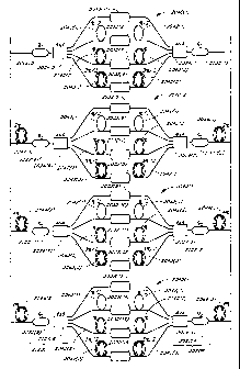
[0050] Figure 38, comprising Figure 38A and 38B, illustrates an alternative
sensor array that includes 16 sensors in an amplified tree-structure telemetry
using a
polarization-based front end similar to the system described above in
connection with
Figures 30-36;
[0051] Figure 39A illustrates the returned pulse train measured at one of the
detectors in Figure 38A for a pulse width of 50 nanoseconds and a repetition
frequency of 0.942 MHz (1.06-microsecond spacing;
[0052] Figure 39B illustrate the returned pulse train measured at one of the
detectors in Figure 38A for a pulse width of 50 nanoseconds and a repetition
frequency of 1.042 MHz (0.96-microsecond spacing);
[0053] Figure 40A illustrates an oscilloscope trace representing the measured
power detected from one of the sensors in Figure 38B when a peal-to-peak phase
modulation of greater than 7t is induced in a PZT transducer in series with
the sensor;
[0054] Figure 40B illustrates the results of measuring the visibility of the
sensor
in accordance with Figure 40A for eight random settings of a common
polarization
controller positioned in one of the input/output fibers of the array in Figure
38B;
[0055] Figure 41 illustrates the results of measurement of the detected
response
from a single detector configuration when a fiber wrapped PZT is used to
simulate an
acoustic signal and an amplitude modulation at 3.6 kHz was placed on the
optical
signal from the source using a lithium niobate modulator in the signal path
from the
source to the collimator in Figure 38A;
CA 02457325 2004-02-09
WO 03/014774 PCT/US02/25228
12
[0056] Figures 42A, 42B and 42 C illustrate the effects of source power on the
measured noise at the detector (receiver) as a function of sensor count for DC
source
currents of 1.4 A, 4.05 pA and 9.89 A, respectively;
[0057] Figure 43A illustrates a plot of the minimum detectable acoustic signal
in a
1-second integration time and also illustrates a plot of the maximum
detectable signal
defined as that which produces a 1 rad/ Hz phase signal for a delay time
through the
delay loop of 50 microseconds;
[0058] Figure 43B illustrates a plot of the minimum detectable acoustic signal
in a
1-second integration time and also illustrates a plot of the maximum
detectable signal
defined as that which produces a 1 rad/ Hz phase signal for the same
parameters as
in Figure 43A but for a delay time through the delay loop of 500 nanoseconds;
[0059] Figure 44A illustrates the phase variation in a sensor caused an
acoustic
signal applied to one of the sensors of Figure 38B;
[0060] Figures 44B and 44C are plots of the induced phase difference due to
the
phase signal of Figure 44A for the signal which travels through the longer
delay loop
(Figure 44B) and the shorter delay loop (Figure 44C);
[0061] Figures 45A illustrates a front end for an acoustic sensor array, which
is
similar to the front end of Figure 38A except that the front end of Figure 45A
includes
a first signal source that outputs an first sequence of optical signal pulses
at a first
wavelength k, and includes a second signal source that outputs a second
sequence of
optical signal pulses at a second wavelength X2, and includes a first delay
loop for the
optical signal pulses at the first wavelength and a second delay loop for the
optical
signal pulses at the second wavelength;
[0062] Figure 45B illustrates an acoustic sensor array connected to the front
end
of Figure 45A;
[0063] Figure 46A is a plot of the signal from a given sensor that passes
through
the longer delay loop of Figure 45A;
CA 02457325 2004-02-09
WO 03/014774 PCT/US02/25228
13
[0064] Figure 46B illustrates the use of linear extrapolation to predict a
fringe
count of (3(2i) from the plot of Figure 46A; and
[0065] Figure 47 is a plot of the maximum value of A before fringe count
errors
occur as a function of frequency for Td' = 100 microseconds, c = 50
microseconds,
and for Td" = 100 nanoseconds.
Detailed Description of the Preferred Embodiments
[0066] The present invention is described below in connection with an array of
acoustic sensors (e.g., hydrophones) in a Sagnac loop. Before describing the
preferred
embodiments, a brief review of the operation of a single loop Sagnac acoustic
sensor
is provided.
Single Loop Sagnac Acoustic Sensor
[0067] A simple Sagnac-based acoustic sensor 100 is shown in Figure 1. The
Sagnac loop is divided into two portions, a delay loop 102 and a hydrophone
104.
The delay loop 102 is simply a large length of fiber, typically greater than 1
km. The
hydrophone 104 is a portion of fiber in which an acoustic wave is transformed
into a
phase modulation of an optical signal propagating through the fiber. A high
responsivity to acoustic waves is typically accomplished by selecting
optimized
coatings for the section of fiber in the hydrophone 104, and wrapping the
fiber around
a mandrel of suitable composition. (See, for example, J.A. Bucaro, et al.,
Optical
fibre sensor coatings, Optical Fiber Sensors, Proceedings of the NATO Advanced
Study Institute, 1986, pp. 321-338.) The length of fiber wrapped around the
hydrophone 104 is typically 10 meters to 100 meters. Light from a source 110,
such
as, for example, a superfluorescent fiber source (SFS), is split into
clockwise (CW)
and counter-clockwise (CCW) beams by a 3x3 coupler 112. The operation of the
3x3
coupler 112 is well-known and is described, for example, in Sang K. Sheem,
Fiber-
optic gyroscope with [3x3] directional coupler, Applied Physics Letters, Vol.
37,
No. 10, 15 November 1980, pp. 869-871.
[0068] Although described herein as using a 3x3 coupler 112, other couplers
(e.g.,
a 2x2 coupler, a 4x4 coupler, etc.) can be used with alternative embodiments
of the
CA 02457325 2004-02-09
WO 03/014774 PCT/US02/25228
14
present invention. For example, to use a 2x2 coupler, both ports of one side
are used
to create the Sagnac interferometer. One port of the other side is a detection
port. The
remaining port is used to launch light into the array and can also be used as
a
detection port if a coupler or circulator is employed (in a similar manner as
is done
with fiber optic gyroscopes). In general, any nxm coupler can be employed by
using
two ports of one side of the coupler to create the Sagnac interferometer and
using the
ports on the other side of the coupler as detection ports, launching ports, or
both.
[00691 After splitting, the CW beam travels through the delay loop 102 first
and
then through the hydrophone 104, while the CCW beam travels through the
hydrophone 104 first and then through the delay loop 102. During a time delay
Tdelay between a time when the CW beam travels through the hydrophone 104 and
a
time when the CCW beam travels through the hydrophone 104, the acoustic signal
and likewise the acoustically induced phase modulation in the hydrophone 104
changes. This change in phase modulation is mapped into a phase difference
between
the counter-propagating beams, which is converted into an intensity modulation
when
the beams recombine at the 3x3 coupler 112. This intensity modulation is then
detected by a first detector 120 and a second detector 122 or by only one of
the two
detectors.
[00701 More explicitly, if an acoustic signal induces a phase modulation
q5hcos(Qt) in the fiber of the hydrophone 104, the resulting phase modulation
between
the interfering beams at the hydrophone 104, Olnr(t), is given by:
Y'!nt(t) _ Oh cOS(SZt)- Oh cOS(Q(t+Tdela ))
Y
2
= 20h sink _ 2delay / sins Qt + n delay
) (1)
where Tdelay is the travel time through the delay loop. Thus, 0nt(t) is a
function of
the hydrophone modulation oh and the product of the acoustic modulation
frequency,
0, with the loop delay, Tdelay. This differs from a Mach-Zehnder
interferometric
sensor in which q$int(t) is a function of only the hydrophone modulation oh.
Maximum
sensitivity is achieved in the Sagnac loop acoustic sensor when the product of
the
CA 02457325 2004-02-09
WO 03/014774 PCT/US02/25228
acoustic frequency, 0, and the time delay, Tdelay, is an odd multiple of it
(maximum
value of the first sine term in Equation 1). The acoustic frequency which
makes this
product it is called the proper frequency of the loop, which is the lowest
frequency at
which maximum sensitivity is achieved. Most underwater sensing applications
are
concerned with the detection of acoustic frequencies below 10 kHz. For the
proper
loop frequency to be less than 10 kHz, a delay time of at least 50
microseconds and
therefore a delay loop length of at least 10 km is required. Thus, the Sagnac
acoustic
sensor 100 requires a large amount of fiber for the detection of low acoustic
frequencies (<10 kHz).
[0071] The common-path design inherent to the Sagnac interferometer has many
advantages over a Mach-Zehnder interferometer in addition to the stable bias
point
and elimination of phase noise already mentioned. A Sagnac interferometer
allows
the use of a short-coherence length, broadband source, such as a
superfluorescent fiber
source (SFS), an example of an amplified spontaneous emission (ASE) source.
Such
sources are inexpensive and can readily provide high powers. It has been shown
that
the use of the 3x3 coupler passively biases the Sagnac acoustic sensor near
quadrature. (See, Sang K. Sheem, Fiber-optic gyroscope with [3 x3] directional
coupler, Applied Physics Letters, Vol. 37, No. 10, 15 November 1980, pp. 868-
871;
and H. Poisel, et al., Low-cost fibre-optic gyroscope, Electronics Letters,
Vol. 26,
No. 1, 4" January 1990, pp. 69-70.) By subtracting the signals from the two
detection
ports of the 3x3 coupler, the source excess noise, which is the limiting noise
source of
SFS sources, can be subtracted while phase-modulation induced intensity
variations
due to the hydrophone are added. This allows a Sagnac interferometer to
approach
near shot-noise limited performance. (See, Kjell Krakenes, et al., Sagnac
interferometer for underwater sound detection: noise properties, OPTICS
LETTERS,
Vol. 14, No. 20, October 15, 1989, pp. 1152-1145.)
[0072] Previous work on Sagnac-based acoustic sensors has been limited to a
single sensor configuration. Because of the inherent advantages of the Sagnac
interferometer, Applicants have determined that it is desirable to replace the
Mach-
Zehnder interferometric sensors in a large-scale array with Sagnac based
sensors.
CA 02457325 2004-02-09
WO 03/014774 PCT/US02/25228
16
Each Sagnac sensor 100 discussed above requires many kilometers of fiber,
making
the insertion of numerous such sensors into a large-scale array impractical.
Research
into using recirculating delay loops to reduce the fiber length requirement
has
produced sensors which use significantly less fiber but suffer from high noise
due to
the incorporation of EDFAs within the recirculating loop. (See, for example,
J.T. Kringlebotn, et al., Sagnac Interferometer Including A Recirculating Ring
With
An Erbium-doped Fibre Amplifier, OFS `92 Conference Proceedings, pp. 6-9.) A
novel approach for decreasing the fiber required is described below.
Novel Sensor Array Based on the Sagnac Interferometer
[0073] As set forth below, Applicants have discovered a novel system which
reduces the amount of fiber needed for a Sagnac-based large scale array by
multiplexing multiple sensors onto the same delay loop, producing a practical
Sagnac
sensor array (SSA). As illustrated in Figure 2, a Sagnac sensor array 200 in
accordance with the present invention includes an array 210 of hydrophones
212(i) in
a ladder configuration which are attached to a single delay loop 214. For
example,
Figure 2 shows a Sagnac sensor array 210 having N hydrophones 212(1), 212(2)
...
212(N) in respective rungs 216(1), 216(2) ... 216(N). Each rung 216(i) in the
Sagnac
sensor array 210 comprises a single fiber wrapped around a respective
hydrophone
212(i). Every path from a 3x3 coupler 220 through the delay loop 214 and array
210
and back to the coupler 220 comprises a separate Sagnac interferometer.
Therefore,
for an array of N sensors 212, there are N separate Sagnac interferometers,
each of
which behaves like the single loop Sagnac sensor 100 shown in Figure 1. Each
Sagnac interferometer measures the acoustic signal at a separate point in
space, i.e.,
the location of the hydrophone 212(i). For example, the Sagnac interferometer
comprising the delay loop 214 and the rung 216(1) measures the acoustic signal
at
hydrophone 212(1). In addition, each Sagnac interferometer also picks up
acoustic
signals (e.g., noise) elsewhere in the loop, which noise is advantageously
reduced, as
will be discussed below.
[0074] The Sagnac sensor array 200 is easiest understood in a time-division
multiplexed (TDM) configuration (non-TDM schemes are discussed later). A
source
CA 02457325 2004-02-09
WO 03/014774 PCT/US02/25228
17
222 (which may advantageously comprise a conventional pulsed source or may
comprise a cw source with an external modulator) generates a light pulse which
enters
the Sagnac loop via a third port of the coupler 220 and propagates in both the
CW and
CCW directions as indicated in Figure 2. Upon reaching the array 210, the CCW
pulse is split into a train of N separate pulses. At this point, the CW input
pulse has
not yet reached the array 210 and is still a single pulse. When the CW pulse
reaches
the array 210, it also is split into a train of N pulses. Each pulse in the CW
train
returns to the 3x3 coupler 220 after traveling through a respective rung
216(i) and
interferes with the pulse in the CCW train which has traveled the same rung
216(i) in
the opposite direction. Thus, N pulses are detected by a first detector 230
and a
second detector 232, and each pulse comprises the CW and CCW pulses of one of
the
N Sagnac loops (i.e., the two pulses which have traveled in opposite
directions
through the same respective rung 216(i)). Because the pulses which travel
through
different combinations of rungs do not travel identical optical paths, such
pulses are
not coincident in time at the coupler 220, and thus do not interfere with each
other at
the coupler 220. The pulse widths should be smaller than the differential
delay
between adjacent sensors so that the pulses from adjacent sensors do not
overlap.
[0075] As illustrated in Figure 3, small-gain erbium doped fiber amplifiers
(EDFAs) 240 are advantageously added to the array portion 210 just as EDFAs
have
been added to Mach-Zelmder interferometric sensor arrays. (See, for example,
Craig W. Hodgson, et al., Optimization of Large-Scale Fiber Sensor Arrays
Incorporating Multiple Optical Amplifiers-Part I: Signal-to-Noise Ratio,
JOURNAL
OF LIGHTWAVE TECHNOLOGY, Vol. 16, No. 2, February 1998, pp. 218-223;
Craig W. Hodgson, et al., Optimization of Large-Scale Fiber Sensor Arrays
Incorporating Multiple Optical Amplifiers-Part II: Pump Power, JOURNAL OF
LIGHTWAVE TECHNOLOGY, Vol. 16, No. 2, February 1998, pp. 224-231;
Jefferson L. Wagener; et al., Novel Fiber Sensor Arrays Using Erbium-Doped
Fiber
Amplifiers, JOURNAL OF LIGHTWAVE TECHNOLOGY, Vol. 15, No. 9,
September 1997, pp. 1681-1688; and C.W. Hodgson, et al., Large-scale
interferometric fiber sensor arrays with multiple optical amplifiers, OPTICS
CA 02457325 2004-02-09
WO 03/014774 PCT/US02/25228
18
LETTERS, Vol. 22, No. 21, November 21, 1997, pp. 1651-1653.) The EDFAs 240
increase the number of sensors which can be supported by a single array 210 by
regenerating the signal power which is lost to coupling and dissipative
losses. The
EDFAs are advantageously pumped by one or more pump laser sources 242 via a
splitting coupler 244 and via a first wavelength division multiplexing (WDM)
coupler
246 and a second WDM coupler 248.
[0076] Because it uses the Sagnac architecture, the Sagnac sensor array 200
has
all of the advantages of the single loop Sagnac based sensor 100 discussed
above.
The common-path design eliminates the conversion of source phase noise into
intensity noise at the interfering coupler 220. The source 222 can be a fiber
ASE
(amplified spontaneous emission) source (i.e., the SFS discussed above), which
provides high powers inexpensively at 1.55 m. Passive biasing near quadrature
is
achievable for all sensors by using the 3x3 coupler 220. Also, the 3x3 coupler
220
provides a convenient means to detect two interferometric outputs at the
detectors
230, 232, and to use the outputs of the two detectors to subtract source
excess noise.
(See, for example, K. Krakenes, et. al., Sagnac interferometer for underwater
sound
detection: noise properties, OPTICS LETTERS, Vol. 14, 1989, pp. 1152-1154,
which
shows the use of two detectors in combination with a single Sagnac
interferometer.)
[0077] The properties of this novel Sagnac sensor array 200 will be discussed
more specifically below followed by a more detailed discussion of the
frequency
response and dynamic range which result from the use of a Sagnac
interferometer.
Thereafter, a calculation of the magnitude of the distributed pick-up from the
non-
hydrophone fiber loop segments will be described, along with a technique for
reducing this pick-up magnitude. Polarization will also be addressed below.
New
sources of noise which are introduced by the Sagnac design are then discussed.
Finally, multiplexing schemes other than TDM for the Sagnac sensor array are
presented.
[0078] Although the present invention is described above with respect to a
single
sensor in each rung 216(i) of the array 210, it should be understood that each
rung
216(i) may advantageously comprise a subarray having multiple sensors, such as
are
CA 02457325 2004-02-09
WO 03/014774 PCT/US02/25228
19
described, for example, in allowed U.S. Patent Application No. 08/814,548,
filed on
March 11, 1997, which is incorporated by reference herein. (See, also, C.W.
Hodgson, et al., Large-scale interferometric fiber sensor arrays with multiple
optical
amplifiers, Optics Letters, Vol. 22, 1997, pp. 1651-1653; J.L. Wagener, et
al., Novel
fiber sensor arrays using erbium-doped fiber amplifiers, Journal of Li hg
twave
Technology, Vol. 15, 1997, pp. 1681-1688; C.W. Hodgson, et al., Optimization
of
large-scale fiber sensor arrays incorporating multiple optical amplifiers,
Part I:
signal-to-noise ratio, Journal of Lightwave Technology, Vol. 1.6, 1998, pp.
218-223;
and C.W. Hodgson, et al., Optimization of large-scale fiber sensor arrays
incorporating multiple optical amplifiers, Part II: pump power, Journal of Li,
htwave
Technology, Vol. 16, 1998, pp. 224-23 1.)
Frequency Response
(00791 As set forth above, the Sagnac sensor has a frequency dependent
response
given by Equation 1. At frequencies well below the proper frequency of the
loop,
defined as 1/(2=Tdelay), the minimum detectable acoustic signal scales with
the inverse
of acoustic frequency. This decreased acoustic sensitivity at low frequencies
has been
a major concern for the Sagnac acoustic sensor. However, it has been pointed
out that
this decreased sensitivity at low frequencies is fortunately matched by an
increasing
ocean noise floor (See, for example, Sverre Knudsen, Ambient and Optical Noise
in
Fiber-Optic Interferometric Acoustic Sensors, Fiber-Optic Sensors Based on the
Michelson and Sagnac Interferometers: Responsivity and Noise Properties,
Thesis,
Chapter 3, Norwegian University of Science and Technology, 1996, pp. 37-40.)
Ideally, it would be desirable if the minimum detectable acoustic signal of an
array at
a given frequency were to be a constant amount below the ocean noise floor at
that
frequency. Thus, the minimum detectable acoustic signal would also increase at
lower frequencies to match the increasing ocean noise floor. The frequency
response
of the Sagnac sensor array 200 of the present invention in fact does provide a
good
match between the ocean noise floor and acoustic sensitivity. This is
illustrated in
Figure 4, where the minimum detectable acoustic signal for a Sagnac sensor
array is
plotted as a curve 250 assuming an optical noise floor of 10 rad/ Hz , a
hydrophone
CA 02457325 2004-02-09
WO 03/014774 PCT/US02/25228
phase responsivity of 3.2 x 10-' rad/.tPa and a delay loop length of 20 km.
(The
vertical axis is in dB relative to a baseline of 1 rad/ Hz .) Also plotted in
Figure 4
are the ocean noise floors for the three dominant ocean noise sources at these
frequencies and a resulting sum of the noise from the three sources. A curve
252
represents the noise from ocean turbulence, earthquakes, volcanic eruptions,
and the
like. A curve 253 represents light shipping noise. A curve 254 represents DSSO
(distant shipping and storms) noise. A curve 256 represents the sum of the
noise
floors from the three dominant sources (i.e., the sum of the curves 252, 253
and 254).
(See, for example, Robert J. Urick, The noise background of the sea: ambient
noise
level, Principles of Underwater Sound, 3rd Ed., Chapter 7, McGraw-Hill, 1983,
pp.
202-236.) The minimum detectable acoustic signal of the Sagnac sensor array
200
increases in such a way as to provide a nearly constant amount of detectable
signal
below the ocean noise floor at all frequencies below 10 kHz. Thus, the
frequency-
dependent response of the Sagnac sensor array 200 does not prohibit low-
frequency
acoustic detection. The Mach-Zehnder array shows the same trend as the Sagnac
sensor array, namely a decreasing sensitivity towards lower frequencies, but
in the
Mach-Zehnder array, the decreasing sensitivity is smaller than in the Sagnac-
based
sensor.
[0080] Although both the Mach-Zehnder interferometer and Sagnac sensor array
200 have similar frequency-dependent responses, the source of their frequency
responses is fundamentally different. The increasing minimum detectable signal
in
the Mach-Zehnder interferometer sensor array is due to an increasing optical
noise
floor. The cause of this increasing optical noise floor is the phase noise
introduced by
the path-imbalanced Mach-Zehnder interferometer. Thus, although the noise
floor is
10 grad/ Hz at 10 kHz, it increases towards lower frequencies. In the Sagnac
sensor
array 200, the increasing minimum detectable acoustic signal is due to the
sin(QTdelay/2) term in Equation 1, and not to an increasing optical noise
floor. The
optical noise floor remains a constant 10 rad/ Hz over the entire frequency
range.
[0081] The significance of this difference can be seen by examining the
dynamic
range of the Mach-Zehnder interferometric sensor array and Sagnac sensor array
200,
CA 02457325 2004-02-09
WO 03/014774 PCT/US02/25228
21
illustrated in Figure 5. The dynamic range of a sensor is limited by the
minimum and
maximum detectable phase shifts. For interferometric sensors, the maximum
detectable phase shift is limited by the nonlinear response of the
interferometer and
the minimum detectable phase shift by the optical noise floor. Both the Mach-
Zehnder interferometric sensor array and the Sagnac sensor array have maximum
detectable phase shifts which are constant over the acoustic frequency range.
However, the Sagnac sensor array 200 also has a flat minimum detectable phase
shift
because it has a flat optical noise floor, while the Mach-Zehnder
interferometric
sensor array suffers an increasing minimum detectable phase shift due to an
increasing
optical noise floor caused by the phase noise introduced by the path
imbalanced
interferometer. The Sagnac sensor array 200 thus has a constant dynamic range
at all
acoustic frequencies, while the Mach-Zehnder interferometric sensor array has
a
decreased dynamic range at low acoustic frequencies. This is illustrated in
Figure 5,
wherein the minimum and maximum detectable acoustic signals (in dB arbitrary
units) are plotted for the Sagnac sensor array 200 and a Mach-Zehnder
interferometric
sensor array. As shown in Figure 5, both arrays have an approximately 100 dB
dynamic range above 1 kHz, where phase noise does not limit the Mach-Zehnder
interferometric sensor array. At 10 Hz, phase noise dominates the Mach-Zehnder
interferometric sensor array, and its dynamic range is reduced to
approximately 74
dB. Meanwhile, the dynamic range of the Sagnac sensor array 200 remains at
approximately 100 dB.
[0082] It is interesting to examine the frequency response of the Sagnac
sensor
array 200 at frequencies well below the loop proper frequency as a function of
the
delay loop length and hydrophone responsivity. At these frequencies, the
sin(S2Tdelay/2) factor in Equation 1 can be approximated as S2Tdelay/2,
showing that
the responsivity of the Sagnac sensor array 200 is proportional to the product
of jh
and Tdelay= 4 itself is proportional to the amount of fiber in each hydrophone
212(i),
and Tdelay is proportional to the amount of fiber in the delay loop 214. Thus,
the
responsivity at frequencies well below the loop proper frequency is
proportional to the
product of the hydrophone fiber length and delay fiber length. Figure 6 plots
the
CA 02457325 2004-02-09
WO 03/014774 PCT/US02/25228
22
minimum detectable acoustic signal for several Sagnac sensor array
configurations in
which the product of the length of the fiber in each hydrophone 212(i) and the
length
of the fiber in the delay loop 214 is constant, but the relative distribution
of fiber
between the delay loop 214 and each hydrophone 212(i) changes. For example, a
curve 260 represents the frequency response of a Sagnac sensor array 200
having 45
km of fiber in its delay loop 214 and 100 meters of fiber in each hydrophone
212(i); a
curve 262 represents the frequency response of a Sagnac sensor array 200
having 30
km of fiber in its delay loop 214 and 150 meters of fiber in each hydrophone
212(i);
and a curve 264 represents the frequency response of a Sagnac sensor array 200
having 15 km of fiber in its delay loop 214 and 300 meters of fiber in each
hydrophone 212(i). As illustrated, each Sagnac sensor array 200 has the same
sensitivity at low frequencies, but approaches a maximum sensitivity at
different
frequencies given by their respective loop proper frequencies. Thus, for a
given
minimum detectable acoustic signal at low frequencies, there is still some
freedom in
choosing the fiber lengths of the delay loop 214 and the hydrophones 212(i).
This
freedom may be used to help the Sagnac sensor array 200 satisfy other
criteria, such
as minimizing the total amount of fiber required or minimizing the delay loop
length.
Increasing the Dynamic Range of the Sagnac sensor array
[0083] As discussed above, the Sagnac sensor array 200 has a larger dynamic
range at low acoustic frequencies than the Mach-Zehnder interferometric sensor
array
because it is immune to phase noise. Ideally, an array 200 provides enough
dynamic
range to detect the strongest and weakest acoustic signal which are likely to
be
encountered. This requirement often translates into a required dynamic range
of
approximately 150 dB. In order to achieve such a large dynamic range in a Mach-
Zehnder interferometric sensor array, two separate sensors with different
phase
responsivities are required, with each detecting a fraction of the total 150
dB dynamic
range. The obvious disadvantage to this scheme is that it requires two sensor
arrays
(i.e., twice as many hydrophones, rungs, sources and detectors). Effectively,
an array
which can support N hydrophones can detect the acoustic signal at only N/2
points.
CA 02457325 2004-02-09
WO 03/014774 PCT/US02/25228
23
[0084] In the Sagnac sensor array 200, it is possible to achieve a large
dynamic
range without using additional hydrophones 212. Because the phase responsivity
in
the Sagnac sensor array is a function of the hydrophone responsivity and delay
loop
length, as shown in Equation 1, the phase responsivity of the entire array of
hydrophones can be changed by modifying the delay loop length. By
simultaneously
using two separate delay loops 214(1) and 214(2) of length L1 and L2,
respectively, as
shown in a modified sensor array 266 in Figure 7, the detection range of the
array 266
can be dramatically increased. The array 266 now has 2N separate Sagnac loops.
Each hydrophone 212(i) returns a separate signal for each of the two delay
loop paths,
and the length of each delay loop 214(1), 214(2) determines the acoustic
detection
range of that signal. The total acoustic detection range of each hydrophone
212(i) is
the union of the detection ranges of each of the two Sagnac loop sensors which
enclose the hydrophone 212(i). The lengths of L1 and L2 set the acoustic
detection
range. The length L1+L2 is chosen to allow the array 266 to detect the
smallest
acoustic signal of interest. The length L, of the delay loop 214(1) is then
chosen to
place the detection range of the signals which travel only this shorter delay
loop on
top of the detection range of the signals which travel both delay loops
214(1), 214(2).
In a TDM system, as a result of the insertion of a second loop, the repetition
frequency of the source pulses are halved in order to allow time for 2N pulses
to
return, and the lengths of the delay loops 214(1), 214(2) are chosen such that
there is
no pulse overlap. Because the repetition frequency is halved, the dynamic
range of
each individual signal decreases by 3 dB. This decrease is more than offset by
the
increase in the total dynamic range achieved by piggybacking the dynamic range
of
two separate signals. In Figure 7, the second delay loop 214(2) is positioned
such that
all light passing through the second delay loop 214(2) passes through the
first delay
loop 212(1). It should be understood that, alternatively, the two delay loops
214(1),
214(2) can be optically in parallel such that the light which passes through
the second
delay loop 214(2) does not pass through the first delay loop 214(1). In such
case, the
fiber length of the second delay loop 214(2) would have to be the sum of the
first
length and the second length (i.e., L1+L2). But, since L1 is considerably
shorter than
CA 02457325 2004-02-09
WO 03/014774 PCT/US02/25228
24
L2, this adjustment is not essential. The embodiment of Figure 7 reduces the
total
fiber requirements by adding the length of the first delay loop to the second
delay
loop.
[0085] Figure 8 illustrates the extended dynamic range made possible by using
the
two delay loops 214(1), 214(2) in the array 266 in which the dynamic range of
each
signal is 100 dB and the ratio L1/L2 was set to be 5000. As shown, the array
266 is
now able to detect over the entire dynamic range of interest (approximately a
160-dB
range) without increasing the hydrophone count.
Distributed Sensing
[0086] In the Sagnac sensor array 266, any phase modulation in the
interferometer
can be transferred into an intensity modulation at the interfering 3x3 coupler
220.
This distributed sensing over the entire Sagnac loop is disadvantageous for an
acoustic
sensor array. In order to be practical, the acoustic sensor array should
sample the
acoustic signal at a number of discrete points in space (i.e., at the
hydrophones) and
return these signals independently. Mach-Zehnder interferometric sensor arrays
achieve this because the interferometer is confined within a small space and
thus only
senses at that point. In order for the Sagnac sensor array 266 to be
practical, the
distributed sensing of the Sagnac loop must be decreased.
[0087] The bulk of the fiber in the interferometer constitutes the delay loop
214,
which can be located in two positions. The first is with the source 222 and
the
detection electronics (i.e., the detector 230 and the detector 232) in the dry
end (i.e.,
out of the water), as shown in Figure 9A. Here the delay loop 214 can be
environmentally shielded to minimize any external modulation. However,
downlead
fibers 270, 272 which connect the wet end to the array portion 210 are part of
the
interferometer. The second possibility is to locate the delay loop 214 in the
wet end
(i.e., in the water) with the array 210, as shown in Figure 9B. As such, the
delay loop
214 cannot be isolated to the same extent as it could if it were located in
the dry end,
but the downlead fibers 270, 272, 274 are outside of the interferometer and
thus are
non-sensing. The relative magnitude of the downlead and delay loop distributed
pick-
up dictates which configuration is best suited for a particular application.
It should be
CA 02457325 2004-02-09
WO 03/014774 PCT/US02/25228
noted that if the delay loop 214 is located in the dry end (Figure 9A), the
downlead
fibers 270, 272 must remain stationary to prevent physical movements, such as
bending and vibrations, of these fibers, which can induce extremely large
phase
modulations. These are fiber motion induced phase modulations as opposed to
acoustically-induced phase modulations. (Such physical movements are problems
in
towed arrays, but may not be significant problems in stationary arrays.) Thus,
if the
delay loop 214 is located in the dry end (Figure 9A), the entire wet end of
the Sagnac
sensor array 210 must be stationary. However, with the delay loop 214 located
in the
wet end (Figure 9B), only the portion to the right of the 3x3 coupler 220 in
Figure 9B
must remain stationary since the downlead fibers 270, 272, 274 are not then
part of
the interferometer. When the delay loop 214 is located in the wet end (Figure
9B), the
delay loop fiber must be desensitized. The delay loop 214 can be made
stationary by
wrapping the delay loop fibers around a desensitized cylinder (not shown),
thereby
eliminating fiber motion and making acoustic pick-up the dominant source of
distributed pick-up signal. Because it is easier to desensitize fiber to
acoustically-
induced phase modulation than it is to desensitize fiber to movement-induced
phase
modulation, the configuration which locates the delay loop 214 in the wet end
(Figure
9B) is preferable for towed array applications and will be described in more
detail
below.
Calculation of the Acoustic Pick-up Noise Induced in the Delay Loop
100881 In this section, estimates are derived for the magnitude of the
acoustically
induced distributed pick-up noise as compared to the acoustically induced
hydrophone
phase modulation in the Sagnac sensor array 210 of Figure 9(b). The intensity
modulation due to the distributed phase modulations resulting from the pick-up
of
acoustic signals in the delay loop and bus fiber (the fiber connecting each
hydrophone
to the delay loop and the 3x3 coupler) can be considered a source of noise.
For the
following discussion, consider one loop of the Sagnac sensor array as
comprising only
delay fiber of length Ld, a bus fiber of length Lb, a hydrophone fiber of
length Lh, and
a total length L, as shown in Figure 10. Also assume that Ld is much larger
than Lb
and Lh. The phase responsivity of fiber to acoustic signals results from a
pressure
CA 02457325 2004-02-09
WO 03/014774 PCT/US02/25228
26
dependent propagation constant, P. In general, the pressure dependent
component of
the propagation constant at a position l and time t can be written as:
,8(l,t) = f0R(l)P (I,t) (2)
where P. is the zero-pressure propagation constant, R(l) is the normalized
phase
responsivity of the fiber, and P(l,t) is the pressure as a function of space
and time. If a
sinusoidal acoustic signal of frequency Q is assumed, Equation 2 can be
rewritten as:
/3(l,t) _ /30R(1)[P0 + P,,, sin(S2t + 0(1))] (3)
where PO is the steady-state pressure, Pm is the amplitude of the pressure
modulation
(assumed to be independent of 1), and 0(l) contains the spatial phase
variation of the
acoustic wave. In general, the induced phase difference between interfering
beams in
a Sagnac loop due to acoustically induced phase modulation from 1=11 to 1=12
is
given by the integral:
0,~t (t) = f2 /3I 1, t + (l - L)1 _ ~(1, t - l I dl (4)
V v)))
where v is the speed of light in the fiber, and L is the loop length.
Substituting
Equation 3 into Equation 4 yields:
A.,(t)=/30Pf R(1) sin SZ(t+1 vL)+0(1) -sin (t-v)+0(1) dl (5)
Equation 5 can be used to determine the phase difference between interfering
beams
due to acoustic modulation of the hydrophone, bus, and delay fibers.
[0089] For the hydrophone fiber, Equation 5 is integrated from 11=1d+1b/2 to
12=ld+lb/2+lh. It is assumed that 0(l) is constant over this range (i.e., that
the
acoustic wavelength is much larger than the dimension of the hydrophone). It
is also
assumed that the normalized phase responsivity of the fiber, R(l), is constant
and is
equal to Rh in this range. Equation 5 then gives a phase difference amplitude
between
interfering beams due to hydrophone fiber modulation:
S2=T (6)
h delay
~;n, = 2/30RhP.Lh sin 2
CA 02457325 2004-02-09
WO 03/014774 PCT/US02/25228
27
where it is assumed that c2Lh/2v <<1. Note that Equation 2 agrees with the
expression
given in Equation 1.
[0090] For the bus fiber, Equation 5 is integrated first from 11=1d to
l2=ld+lb/2,
and then from 11=L-lb/2 to 12=L to include both the upper and lower bus lines.
Again,
it is assumed that R(l) is constant and equal to Rb for all bus fiber, such
that 0(l) is
constant in the integral of Equation 5. The phase difference amplitude between
interfering beams due to fiber modulation becomes:
b Y int - 2,60 Rb Pr Lb sin delay (7)
2
where it is assumed that S2Lh/2v 1. It should be emphasized that the
assumptions on
the constancy of 0(l) and the amplitude of S2Lh/2v act to increase O nt , thus
giving a
worst case scenario for the bus fiber.
[0091] For the delay fiber, Equation 5 is integrated from 11=0 to 12=1d, and,
as
before, it is assumed that 0(l) is constant over this range (i.e., the delay
loop coil is
much smaller than the acoustic wavelength), and that R(1) is constant and
equal to Rd
over the integral. Equation 5 then yields a phase difference amplitude between
interfering beams due to delay fiber modulation given by:
od = 2,8R P (L - L ) sin QTdelay = 2 ,8 R (Lb + L) sin QTdelay (8)
tnt O d d 2 O d b h 2
where it is assumed that Q(Lb+Lh)/2v 1.
[0092] With Equations 6-8, the relative magnitude of these phase modulations
amplitudes can be computed. First, it is noted that a standard plastic coated
fiber has a
normalized phase responsivity, R, of -328 dB re 1/ Pa, as described, for
example, in
J.A. Bucaro, et al., Optical fibre sensor coatings, Optical Fiber Sensors,
Proceedings
of the NATO Advanced Study Institute, 1986, pp. 321-338. On the other hand, as
described, for example, in C.C. Wang, et al., Very high responsivity fiber
optic
hydrophones for commercial applications, Proceedings of the SPIE-The
International
Society for Optical Engineering, Vol. 2360, 1994, pp. 360-363, a fiber wrapped
around current hydrophones made from air-backed mandrels has a normalized
phase
sensitivity of -298 dB re 1/ Pa, an increase of 30 dB over standard fiber. If
we
CA 02457325 2004-02-09
WO 03/014774 PCT/US02/25228
28
assume that the delay loop and the bus fiber have the normalized phase
responsivity of
standard plastic coated fiber, and that the hydrophone fiber is wrapped around
an air-
backed mandrel, then the ratio of Rh to Rb or Rd is approximately 30 dB.
Therefore,
under the simplifying assumption made to reach Equations 6-8, it can be found
that:
Dint 31
1 + (Lb /Lh) (9)
Oint
and
ant 31 (10)
~/,b
Y'int Lb /Lh
[0093] The ratio Lb/Lh is a function of the hydrophone position. For the first
hydrophone, Lb/Lh z 0 making Y'int / O nt = 31 and Y'int / Oint extremely
large. For the last
hydrophone, typical values of 100 meters and 1 km for Lh and Lb, respectively,
are
used to arrive at ant / Dint = Oint / Oint z 3. Thus, despite the fact that
the hydrophone fiber
constitutes a relatively small amount of the overall Sagnac loop, the
magnitude of the
acoustically induced phase modulations in the hydrophone fiber are greater
than the
acoustically induced phase modulations in the delay loop fiber and in the bus
fiber for
even the furthest hydrophone. The following section describes a means for
dealing
with this level of distributed pick-up noise using empty rungs.
[0094] In order to evaluate the integral in Equation 5 for the delay loop
fiber, it is
assumed that R(1)=Rd for all 1 less than Ld. It was this constancy of R(1)
which
eliminated any contribution to the integral of Equation 5 from 1=(L-Ld) to Ld
(because
the integrand became an odd function about L/2). However, coiling a long
length of
fiber will result in some dependence in R(1) on 1 (possibly because the inner
layer of
fiber has a different R than the outer layer). These variations in R(1)
increase the delay
loop pick-up from 1=L-Ld to Ld. In order to reduce this pick-up, it is first
noted that
R(1) need only be an even function around L/2 to make the integrand of
Equation 5 an
odd function about L/2. R(1) can be forced to be more symmetric about L/2 by
wrapping the delay loop in such a way as to position symmetric points of the
fiber
loop next to each other as shown in Figure 11. Such a wrapping ensures that
symmetric points of the delay loop are positioned in proximity to each other
so that
CA 02457325 2004-02-09
WO 03/014774 PCT/US02/25228
29
any variations in R(1) due to the position of the fiber on the coil are as
symmetric
about L/2 as possible, thereby making the delay loop pick-up as close to the
expression of Equation 8 as possible. Note that, because each Sagnac loop in
the
Sagnac sensor array has a different L/2 point, only one loop can be wrapped
exactly as
shown in Figure 11, thereby introducing a small degree of oddness in R(1) to
all but
one of the Sagnac loops.
[0095] It should also be mentioned that in addition to enhancing the acoustic
sensitivity of fiber with a hydrophone, it is possible to desensitize fibers
by applying a
metallic coating of a particular diameter. (See, for example, J.A. Bucaro,
Optical
fibre sensor coatings, cited above.) Measured normalized phase responsivities
as low
as -366 dB re 1/.tPa have been reported. If such fibers are used in the delay
or bus
lines, the ratio of Rh to Rb or the ratio of Rh to Rd approaches 68 dB
(instead of 30 dB
with plastic coated delay and bus fibers), increasing the hydrophone induced
signal
over the delay and bus induced signal by 38 dB.
Reducing the Distributed Pick-up Noise by Using Empty Rungs
[0096] In order to further eliminate distributed pick-up signal, the
hydrophone-
induced acoustic modulation can be isolated from the distributed pick-up
modulation
by placing empty rungs 300 that do not contain a hydrophone in the array 210,
as
shown in Figure 12. Each rung 216(i) which contains a hydrophone 212(i),
called a
sensing rung, is proceeded by one of the empty rungs 300(i). The fact that the
non-
sensing fiber of each loop which encloses an empty rung 300(i) is nearly
identical to
the non-sensing fiber of the loop which encloses the corresponding sensing
rung
212(i) means the empty rung 300(i) and the corresponding sensing rung 212(i)
will
have nearly the same distributed pick-up signal. By treating this empty rung
300(i) as
another sensor in the array 210 and properly timing the pulses (in the TDM
scheme)
from the empty rungs 300(i) and the sensing rungs 212(i) so that they do not
overlap,
the distributed pick-up signal present on each sensing rung 212(i) can be
measured.
After detection, this signal can be subtracted from the sensing rung signal,
leaving
only intensity variations produced by phase modulations in the hydrophone
fiber.
CA 02457325 2004-02-09
WO 03/014774 PCT/US02/25228
Implementing such a scheme requires 2N rungs for an N sensor array 210,
thereby
reducing the duty cycle of individual signals by one half.
[0097] If desensitizing the bus portion of the array 210 is not required, a
single
empty rung 300 can be placed in the array 210 to measure the distributed pick-
up
signal associated with the delay loop 214, thereby requiring only N+1 rungs (N
sensing rungs 212(i) and one empty rung 300) for N sensors. If one empty rung
300
does not adequately measure the distributed pick-up signal for each sensing
rung
212(i), more empty rungs 300 can be added at periodic intervals along the
array, until
the distributed pick-up signal present on each sensing rung 212(i) can be
adequately
measured by the nearest of these empty rungs 300. Using fewer empty rungs
results
in a higher duty cycle for individual signals. Figure 12 depicts the extreme
in which
an empty rung was added for every sensing rung.
Polarization
[0098] For maximum contrast in any interferometric sensor, the state of
polarization (SOP) of the interfering beams must be identical when they
recombine.
If they are orthogonal, there is no interference and thus no amplitude-
modulated
signal. This is referred to as polarization-induced signal fading. Because
each sensor
in the Sagnac sensor array is a Sagnac loop, the research carried out so far
on
polarization-induced signal fading in the Sagnac fiber gyroscope applies to
the Sagnac
sensor array as well. One promising solution is to place a depolarizer within
the
Sagnac loop. (See, for example, K. Bohm, et al., LOW-DRIFT FIBRE GYRO USING
A SUPERLUMINESCENT DIODE, ELECTRONICS LETTERS, Vol. 17, No. 10,
14th May 1981, pp. 352-353.) The depolarizer ensures that at least half of the
optical
power is returning to the 3x3 coupler in the correct SOP at all times. This
general
approach produces a constant visibility regardless of the loop birefringence.
(See, for
example, William K. Bums, et al., Fiber-Optic Gyroscopes with Depolarized
Light,
JOURNAL OF LIGHTWAVE TECHNOLOGY, Vol. 10, No. 7, July 1992, pp. 992-
999). The simplest configuration uses an unpolarized source such as a fiber
superfluorescence source and a depolarizer in the loop. As illustrated in
Figure 13, in
the Sagnac sensor array 200, one depolarizer 310 is placed at a point which is
CA 02457325 2004-02-09
WO 03/014774 PCT/US02/25228
31
common to all the Sagnac loops. The depolarizer 310 ensures that each sensor
212(i)
has this constant visibility independent of birefringence as long as the loop
birefringence remains constant. This represents a great simplification in the
handling
of polarization-induced signal fading over those methods used in Mach-Zehnder
interferometric sensor arrays.
[0099] Although slow changes in the birefringence will be sufficiently
canceled
by the reciprocal nature of the Sagnac interferometer, birefringence
modulations at
frequencies in the acoustic range of interest will produce polarization noise.
Most
birefringence modulation at these frequencies occurs as a result of physical
fiber
movement. Thus, the Sagnac loop should remain stationary in order to reduce
the
polarization noise (as well as the distributed pick-up signal).
Noise Sources Introduced by the use of the Sagnac Interferometer
Thermal Phase Noise
[0100] Because the index of refraction of the fiber changes with temperature,
thermal fluctuations in a fiber will produce phase fluctuations in the light
traveling
through it. These index variations are uncorrelated over the length of fiber,
and thus
the resulting phase fluctuations scale as the square root of length. Because
Mach-
Zehnder interferometers typically use less than 100 meters of fiber in each
arm, the
magnitude of this thermal phase noise is negligible. The Sagnac interferometer
has a
great deal more fiber in the interferometer and as a result, thermal phase
noise can
become a limiting noise source. The magnitude of this thermal phase noise in a
Sagnac interferometer has been described theoretically and confirmed by
experiment.
(See, for example, Sverre Knudsen, et al., Measurements of Fundamental Thermal
Induced Phase Fluctuations in the Fiber of a Sagnac Interferometer, IEEE
Photonics
Technology Letters, Vol. 7, No. 1, 1995, pp. 90-93; and Kjell Krakenes, et
al.,
Comparison of Fiber-Optic Sagnac and Mach-Zehnder Interferometers with Respect
to Thermal Processes in Fiber, JOURNAL OF LIGHTWAVE TECHNOLOGY,
Vol. 13, No. 4, April 1995, pp. 682-686.). For loops greater than 2 km, the
thermal
CA 02457325 2004-02-09
WO 03/014774 PCT/US02/25228
32
phase noise can exceed 1 rad/ Hz in the frequency range of interest, which is
on
the order of the required array sensitivity.
[0101] The thermal phase noise can be considered as a source of distributed
pick-
up noise, akin to an external modulation to the delay loop, and as such can be
reduced
by using empty rungs, as described above. Thermal phase noise can also be
reduced
by shortening the loop length. As discussed above, the loop length can be
shortened
without changing the low frequency sensitivity by increasing the hydrophone
fiber
length by the same factor as that by which the delay loop was decreased. For
example
a 40-km delay loop with 50 meters of hydrophone fiber has the same low-
frequency
response as a 20-km delay loop with 100 meters of fiber. The latter
combination
however will suffer less thermal phase noise because the total delay loop
length is
shorter by almost a factor of two.
Kerr Effect Induced Phase Noise
[0102] Kerr-induced phase shifts which can be generated in a Sagnac
interferometer have received a great deal of attention for the fiber optic
gyroscope.
(See, for example, R.A. Bergh, et al., Source statistics and the Kerr effect
in fiber-
optic gyroscopes, OPTICS LETTERS, Vol. 7, No. 11, November 1982, pp. 563-565;
R.A. Bergh, et al., Compensation of the optical Kerr effect in fiber-optic
gyroscopes,
OPTICS LETTERS, Vol. 7, No. 6, June. 1982, pp. 282-284; and N.J. Frigo, et
al.,
Optical Kerr effect in fiber gyroscopes: effects of nonmonochromatic sources,
OPTICS LETTERS, Vol. 8, No. 2, February 1983, pp. 119-121.) The demands of the
gyroscope and the acoustic sensor, however, are different because the
gyroscope
measures DC levels. Small DC offsets created by Kerr-induced phase shifts
which
would limit a fiber gyroscope are non-issues with an acoustic sensor. The Kerr-
induced DC phase shift is not a problem as long as it does not move the bias
point too
far away from quadrature. The intensity noise on the light source can produce
a Kerr
induced phase noise on the output. However, the magnitude of this Kerr-induced
AC
phase noise is small as long as the Kerr-induced DC phase shift remains small.
The
origin of Kerr-induced phase shifts in the Sagnac sensor array is different
than in the
fiber gyroscope. The asymmetry of the Sagnac sensor array invites such a Kerr
phase
CA 02457325 2004-02-09
WO 03/014774 PCT/US02/25228
33
shift much more readily than the nominally symmetric gyroscope does. That
asymmetry results from the array portion as well as any placement of EDFAs
which
are asymmetric, in that one beam sees gain before propagating through the
delay loop,
then sees loss, while the counter-propagating beam sees loss, then sees gain.
It is
possible to balance these asymmetries and null the Kerr-induced phase shift by
choosing the proper location for EDFAs in the delay loop. The specifics depend
on
the exact array configuration and which multiplexing scheme is used.
Non-linear phase modulation resulting from the EDFAs
[01031 The population inversions created in the EDFAs induce a phase shift on
the signal light that passes through it. (See, for example, M.J.F. Digonnet,
et al.,
Resonantly Enhanced Nonlinearity in Doped Fibers for Low-Power All-Optical
Switching: A Review, OPTICAL FIBER TECHNOLOGY, Vol. 3, No. 1, January
1997, pp. 44-64.) This phenomenon has been used to produce all-optical
interferometric switches. In a Sagnac sensor array, the EDFAs within the
interferometer create a nonlinear phase shift via the same mechanism.
Variations in
the population inversion due to pump or signal power fluctuations will produce
phase
modulations which will be converted to an intensity noise.
[01041 In order to estimate the magnitude of this noise source, a
determination
must be first made as to how the inverted population responds to pump and
signal
power fluctuations. This is relatively straightforward to do by invoking the
rate
equations for an erbium system:
Nl + N2 = No (11)
a e
d e
I pap Isa.,a Ip6p I., NZ
dt NZ hvpAef Ni + hv,Aef N1 hvpAef. N2 hvsAeff N2 z2
(12)
where N1 and N2 are the population densities of the lower and excited states
respectively, No is the total population density, I is the intensity, a is the
cross section,
Aeff is the effective mode area in the fiber, and i2 is the lifetime of level
two. The
subscripts p and s denote pump and signal, respectively, and the superscripts
a and e
denote absorption and emission, respectively.
CA 02457325 2004-02-09
WO 03/014774 PCT/US02/25228
34
[0105] By splitting N1, N2, Ip, and I. into their steady-state and time-
varying
components, then substituting this into Equation 12 and combining Equation 12
with
Equation 11, the result is:
u a r [Noa; ++6) [Noa: +Ns(6e +)
N2 W Na; P IP (t) + 2 s s Is (t) +
dt hvP hvs
ss( a a) Iss(6e +6a) 1 ( e a)
IP QP + QP + s s s + - N2 (t) - 6P + 6P IP (t)N2 (t) -
h vP hvs z2 hvP
e a
6s + 6s
hvs Is (t)N2 (t,
(13)
where the superscript ss denotes steady-state values, and the time-varying
components
are now written as explicit functions of time (N2=N2SS+N2(t)). If it is
assumed that
N2(t) is much smaller than N2SS, then the last two terms in Equation 13 can be
neglected. By writing Ip(t)=Ipmsin(fpt) and Is(t)=Ismsin(fst) (where Ipm and
Ism denote
the modulation amplitudes of Ip(t) and Is(t), respectively, and fp and fs
respectively
denote the pump and signal modulation frequencies) and solving the resulting
differential equations, it can be found that:
I N2 W P ti 6s (aP + aP )- -or' (6s + 6s) yP 1 I ssI P
N2s (6e +6a)2 vs 1+ f2 /f2 Iss2
P P P P (14)
N2 Vs 6s 6s + 6s VP 1 IM
Nss 6a Qe + 6a v 2 2 Iss
2 P P P s 1+ fP If o p
(15)
where:
e a e a e a
ss 6s + as ss 1 6P + 6P I's Is' ss
I+ Is+- I& I when I>> I.
Ja - hvP P hvs r2 hvP P P Is. (16)
CA 02457325 2004-02-09
WO 03/014774 PCT/US02/25228
[0106] If it is assumed that kp 1480 nm, X5 1550 nm, and Ipss=1 W, and if
typical erbium-silica cross sections are assumed, then Equations 14 and 15
simplify
to:
IN2 `f n l 0.9 I_SI P
Nis 1 + f p /4.3 kHz IP 2
(17)
N24/s 1.2 IS
N2 1 + fs2 /4.3 kHz Ips (18)
[0107] The pump-induced population inversion fluctuations (Equation 17) will
be
analyzed first. If Ipss=1 mW, Ipss=l W, and it is assumed that Ipm/Ipss=10-6/
Hz
(120 dB/ Hz electronic SNR), then IN2(fp)I/N2ss = 9 x 10⁻¹⁰ Hz -1 at
frequencies
well below 4.3 kHz. In order to convert this figure to a phase modulation, the
fact that
10 mW of pump power absorbed in an erbium-doped fiber induces approximately
7 radians of phase shift at 1550 nm can be used. (See, for example, M.J.F.
Digonnet,
et al., Resonantly Enhanced Nonlinearity in Doped Fibers for Low-Power All-
Optical
Switching: A Review, OPTICAL FIBER TECHNOLOGY, Vol. 3, No. 1, January
1997, pp. 44-64.) Using simulations, 10 mW of absorbed pump power in a typical
erbium-doped fiber provides approximately 6 dB of small signal gain at 1550
nm,
which is close to the gain required by each amplifier in an array with
distributed
EDFAs. (See, for example, Craig W. Hodgson, et al., Optimization of Large-
Scale
Fiber Sensor Arrays Incorporating Multiple Optical Amplifiers-Part I. Signal-
to-
Noise Ratio; Craig W. Hodgson, et al., Optimization of Large-Scale Fiber
Sensor
Arrays Incorporating Multiple Optical Amplifiers-Part IT Pump Power; Jefferson
L.
Wagener; et al., Novel Fiber Sensor Arrays Using Erbium-Doped Fiber
Amplifiers;
and C.W. Hodgson, et al., Large-scale interferometric fiber sensor arrays with
multiple optical amplifiers, cited above.) Therefore, each amplifier provides
approximately 7 radians of DC phase shift. Since the nonlinear phase shift is
proportional to the upper state population, N2, it can be written that
AN2/N2ss=A~/ass.
CA 02457325 2004-02-09
WO 03/014774 PCT/US02/25228
36
Using this relation and Equation 17 again for Isss=1 mW, Ipss=1 W,
Ipm1Ipss=10-61Hz and fs 4.3 kHz, the low-frequency phase noise induced by each
EDFA is (7 radians)x(9 x 10⁻¹⁰) Hz -1 = 6.3 x 10⁻⁹ rad/ Hz . If it is assumed
that
there are a total of 500 such amplifiers and that the phase modulations from
all 500
amplifiers add coherently, the total pump noise induced phase shift can be
estimated
to be 3.2 rad/ Hz . The target phase noise floor is typically set to 1 rad/
Hz ,
indicating that the nonlinear phase-noise induced by the EDFAs due to pump
power
fluctuations is close to but not significantly larger than the required phase
noise floor.
In practice, the amplifiers' phase modulations will not add coherently, which
will
reduce the 3.2 Wad/ Hz figure.
[0108] Calculations of the induced phase shift due to signal power
fluctuations are
more complicated because the signal power not only has intensity noise but is
also
modulated by the multiplexing scheme. Again considering the TDM case, in
general,
while a given pulse is traveling through a particular EDFA, there may or may
not be a
counter-propagating pulse traveling through that EDFA at the same time. Taking
the
worst case in which there is always a counter-propagating pulse, Ism is twice
the
intensity noise of each individual pulse. For the amplifiers, Ism is typically
1.5 to 2
times the intensity noise of each individual pulse. Assuming the signal light
has an
electronic SNR of 120 dB/ Hz at acoustic frequencies (i.e., Ism1Isss=10-6/ Hz
), and
inserting this figure into Equation 18 along with Ipss=1 W and Ism=2 mW, it
can be
calculated that 1N2(fs)V1N2ss is approximately 2.4 x 10⁻⁹ Hz -1 at frequencies
much
lower than 4.3 kHz and that the phase noise induced by signal intensity noise
in each
EDFA is thus 1.68 x 10_$ rad/ Hz . Again assuming 500 amplifiers and coherent
addition of all EDFA-induced phase modulation, the total EDFA induced phase
noise
on each pulse is 8.4 rad/ Hz , a level which could again limit the
performance of
the Sagnac sensor array. However, a more detailed study taking into account
the
multiplexing scheme and exact timing of the array is needed for a more
accurate
calculation.
CA 02457325 2004-02-09
WO 03/014774 PCT/US02/25228
37
Multiplexing Schemes in a Sagnac array
Time-Division Multiplexing
[0109] It has been assumed thus far that the Sagnac sensor array is operated
in a
TDM configuration. It should be noted that, in the Sagnac sensor array, the
source
requirements for such a TDM system are not as demanding as those of a Mach-
Zehnder interferometric sensor array in a TDM configuration. The reason for
this is
the use of the broadband source in the Sagnac sensor array. In the Mach-
Zehnder
interferometric sensor array, the light from adjacent rungs is coherent due to
the
narrow linewidth source, and thus extremely high extinction ratios on the
input pulse
are required to prevent multi-path coherent interference. These high
extinction ratio
requirements are achieved by placing multiple modulators in series, which
results in a
complicated, high loss, and expensive source. In the Sagnac sensor array, the
required
extinction ratio need not be as high because the broadband source eliminates
any
possibility of multi-path coherent interference. In addition, the narrow
linewidths
required by the Mach-Zehnder interferometric sensor array prevent the use of a
pulsed
laser source in place of a continuous wave (cw) laser source which is
externally
modulated with Lithium Niobate intensity modulators. In the Sagnac sensor
array,
either a continuous-wave ASE source which is externally modulated, a pulsed
ASE
source, or some combination thereof could be used to construct the source.
Again, the
reason for this is that the Sagnac sensor array does not require a narrow
linewidth
source. Although the present invention does not require a narrow linewidth
source, it
should be understood that the Sagnac sensor array of the present invention can
be used
with a narrow linewidth source, such as, for example, a laser.
Frequency Division Multiplexing
[0110] The use of the broadband source also allows the Sagnac sensor array to
operate in non-TDM configurations without changing the design or requiring
additional sources. Frequency division multiplexing (FDM) is commonly used
with
Mach-Zehnder interferometric sensor arrays using the Phase-Generated Carrier
(PGC)
scheme but is also compatible with the Sagnac sensor array. Figure 14 shows a
basic
CA 02457325 2004-02-09
WO 03/014774 PCT/US02/25228
38
Sagnac sensor array 400 using a FDM scheme. A fiber superfluorescent source
(SFS)
402 (or other broadband source, such as, for example, an LED) generates input
light.
A chirped intensity modulation is applied to the input light via an intensity
modulator
404 which is controlled by a chirped frequency generator 406. The modulated
light
enters a sensor array 410 via a 3x3 coupler 412. The light passes through a
delay loop
414 and plural sensing rungs 416(i) having respective sensors 418(i). Empty
rungs
(not shown) can also be included if desired. After passing through the delay
loop 414
and the rungs 416(i), the light exits from the sensor array 410 through the
coupler 412
and is detected by a detector 420 which generates an electrical output signal
responsive to the detected light. The electrical output signal from the
detector 420 is
mixed in a mixer 422 with the same chirped frequency which has been time
delayed
by a delay 424 which delays the chirped frequency by a time At. In the setup
illustrated in Figure 14, the output of the mixer 422 is applied to a spectrum
analyzer
426. In an operational embodiment, the output of the mixer 422 is applied to a
signal
processing subsystem (not shown) which analyzes the output of the mixer 422 to
reproduce the acoustic signals impinging on the array 410.
[0111] The signals returning from the sensors 418(i) in the various rungs
416(i)
are further delayed with respect to the delayed chirp frequency. This is
illustrated by
the graphs in Figure 15 by the original chirped frequency 450, the delayed
chirped
frequency 452 from the delay 424, the chirped return signal 460 from the first
rung,
the chirped return signal 462 from the second rung and the chirped return
signal 464
from the third rung. In the mixer 422, separate beat frequencies fbl 470, fb2
472,
fb3 474, respectively (shown in Figure 14), are formed between the mixing
chirped
frequency 452 and each of the signals returning from the various rungs in the
Sagnac
sensor array 410. (See, for example, S.F. Collins, et al., A Multiplexing
Scheme For
Optical Fibre Interferometric Sensors Using An FMCW Generated Carrier, OFS `92
Conference Proceedings, pp. 209-211.) Although only three chirped return
signals
460, 462, 464 are illustrated in Figure 15, it is contemplated that up to N
return signals
can be provided, where N is the number of rungs in the array 410. The chirped
return
signals from the Nth rung causes a beat frequency fbN in the mixer 422.
CA 02457325 2004-02-09
WO 03/014774 PCT/US02/25228
39
[01121 As illustrated by a pictorial representation of a spectral output in
Figure 14,
acoustic modulation of the signals will appear as upper sidebands 480, 481,
482 and
lower sidebands 484, 485, 486 to the beat frequencies. An advantage of this
FDM
scheme is that the demands on the array timing are greatly relaxed over those
required
in a TDM system. A TDM system requires a specific delay between adjacent rungs
in
order to prevent pulses from overlapping, and this can present a demanding
engineering problem. In FDM, variations in fiber lengths shift beat
frequencies but do
not induce overlap between signals as long as these beat frequencies are
separated by
twice the acoustic detection range. The latter is accomplished by selecting
the proper
chirp rate. Unlike in a TDM system, all paths return light at all times, which
can
result in phase noise between the different incoherent signals. The broadband
ASE
light source minimizes the magnitude of this phase noise. (See, for example,
Moslehi,
Analysis of Optical Phase Noise in Fiber-Optic Systems Employing a Laser
Source
with Arbitrary Coherence Time, Journal of Lightwave Technology, Vol. LT-4, No.
9,
September 1986, pp. 1334-135 1.)
Code Division Multiplexing
[01131 Code division multiplexing (CDM) has received increased attention
lately
for its use in sensor arrays. (See, for example, A.D. Kersey, et al., Code-
division
Multiplexed Interferometric Array With Phase Noise Reduction And Low
Crosstalk,
OFS `92 Conference Proceedings, pp. 266-269; and H.S. Al-Raweshidy, et al.,
Spread
spectrum technique for passive multiplexing of interferometric optical fibre
sensors,
SPIE, Vol. 1314 Fibre Optics `90, pp. 342-347.) As illustrated for a Sagnac
sensor
array 600 in Figure 16, in CDM, the input light from a fiber superfluorescent
source
602 (or other broadband source, such as, for example, an LED) is modulated in
an
intensity modulator 604 according to a pseudo-random code generated by a code
generator 606. The modulated light is applied to an interferometric loop 608
via a
3x3 coupler 610 and propagates through a delay loop 614 and a plurality of
rungs
616(i) in an array 612. In the illustrated embodiment, each rung 616(i)
includes a
respective sensor 618(i). Empty rungs (not shown) can also be included if
desired.
The light returns from the loop via the 3x3 coupler 610 and is detected by a
detector
CA 02457325 2004-02-09
WO 03/014774 PCT/US02/25228
620. The electrical output of the detector 620 is applied to a correlator 622
along with
the output of the code generator 606, which output is delayed for a duration
ticor by a
delay 624. The bit duration of the pseudo-random code is shorter than the
propagation delay between adjacent rungs in the array 612. When icor is equal
to one
of the loop travel times Ti, through a respective rung 616(i), then the signal
returning
from this sensor in the rung 616(i) is correlated to the delayed pseudo-random
code.
The other signals, which have delays tij where Itij-TtI>tb;t correlate to
zero. The
correlation process involves, for example, multiplying the detected signal by
1 or -1
(or gating the signal in an electronic gate 630 to the non-inverting and
inverting inputs
of a differential amplifier 632) depending on whether the correlating code is
on or off.
The output of the differential amplifier on a line 634 is the correlated
output. The
signal is then time averaged over a period tavg equal to the duration of the
code. The
uncorrelated signals time average to zero, thereby isolating the signal from
sensor
618(i). Tcor is scanned to retrieve sequentially the signals from all sensors.
[0114] An advantage of CDM over TDM is that the delay between sensors does
not have to be controlled accurately. Any loop delays ij in which Itij-ij
1Ihbit is
acceptable (where tibit is the duration of a pulse in the code). Correlating
requires a
knowledge of the tij's, which are easily measured. As with FDM, the use of a
broadband source benefits reducing the phase noise which results from the
addition of
all the signals together.
[0115] The foregoing described a novel design for an acoustic sensor array
based
on the Sagnac interferometer. The major advantages of this design are the use
of
common-path interferometers. This eliminates the conversion of source phase
noise
into intensity noise, which is prevalent in Mach-Zehnder interferometric
sensors, and
allows the use of a cheap, high-power ASE source or other broadband source.
The
response of the Sagnac sensor array as a function of acoustic frequency is
shown to
match the ocean noise floor. The design also allows the dynamic range to be
dramatically increased without adding hydrophones by using one additional,
very
short delay loop. A technique for eliminating polarization-induced signal
fading was
discussed above. The Sagnac sensor array also allows the use of several
multiplexing
CA 02457325 2004-02-09
WO 03/014774 PCT/US02/25228
41
schemes in a simpler form than is achievable with a standard Mach-Zehnder
array.
Because of these features, the Sagnac sensor array design provides a very
promising
alternative to Mach-Zehnder-interferometer-based sensor arrays.
Folded Sagnac Sensor Array
[0116] Figures 17-20 illustrate alternative embodiments of a distributed
acoustic
sensor array based upon the Sagnac effect which has an architecture modified
to
reduce the distributed pick-up from the downlead fibers. In particular, Figure
17
illustrates a basic folded Sagnac acoustic fiber sensor array 700 which
comprises a
source 702, a first detector 704 and a second detector 706. Preferably, the
source 702,
the first detector 704 and the second detector 706 are located in the dry end
of the
sensor array 700 (e.g., on shore or on board a ship).
[0117] The source 702 generates light pulses which are coupled to a 3x3
coupler
710 via a downlead fiber 708. As illustrated, the 3x3 coupler is located in
the wet end
(e.g., proximate to the ocean floor). The 3x3 coupler 710 has a first output
port
coupled to one end of a common fiber rung (rung 0) 712, has a second output
port
coupled to a first array input/output fiber 714 of an array 716, and has a
third output
port which is non-reflectively terminated. Approximately 33 percent of the
light from
the source 702 is coupled to each of the first and second ports of the 3x3
coupler and
thus approximately 33 percent of the light propagates to the common fiber rung
712
and approximately 33 percent of the light propagates to the array 716. As
discussed
above, although described herein as a 3x3 coupler 710, other nxm couplers
(e.g., a
2x2 coupler, a 4x4 coupler, etc.) can be used with the embodiment of Figure 17
and
the alternative embodiments of the present invention described below.
[0118] The array 716 comprises a plurality of rungs 718(i) (i.e., 718(1),
718(2) ...
718(N)) coupled between the first array input/output fiber 714 and a second
array
input/output fiber 720. Each rung 718(i) includes a respective acoustic sensor
(i.e.,
hydrophone) 722(i). The array 716 advantageously includes distributed erbium
doped
fiber amplifiers (EDFAs) 724, such as described above in connection with
Figure 3.
(The pump source for the EDFAs 724 is not shown in Figure 17.) Although
described
CA 02457325 2004-02-09
WO 03/014774 PCT/US02/25228
42
herein with respect to the array 716, other array configurations can also
advantageously be used in the present invention.
[0119] The second array input/output fiber 720 couples the array 716 to a
first
port of a 2x2 coupler 730. A second end of the common rung (rung 0) 712 is
coupled
to a second port of the 2x2 coupler 730. Although described herein as an array
716
comprising plural sensors 722(i), it should be understood that the present
invention
has applications for a sensor system having only a single sensor 722.
[0120] A third port of the 2x2 coupler 730 is nonreflectively terminated at a
terminal 732. A fourth port of the 2x2 coupler 730 is coupled to a delay loop
downlead fiber 740. The delay loop downlead fiber 740 couples the fourth port
of the
2x2 coupler to a first end of a delay loop 750. The delay loop 750 may be
located
either in the dry end as shown or in the wet end. A second end of the delay
loop 750
is coupled to a reflector 752 such that light exiting the second end of the
delay loop
750 is reflected back into the delay loop 750, propagates through the delay
loop 750
and propagates through the delay loop downlead fiber 740 back to the fourth
port of
the 2x2 coupler 730. The light returned from the loop downlead fiber 740 is
divided
by the 2x2 coupler 730 with substantially equal portions propagating in the
common
rung 712 and in the array 716 with both portions propagating toward the 3x3
coupler
710. The two portions are combined in the 3X3 coupler 710 where light pulses
which
have traveled the same distance through the array 716 and through the common
rung
712 interfere and light pulses which have traveled different distances do not
interfere.
The signals resulting from the interference are output from the 3x3 coupler
710 as
first and second output signals which respectively propagate to the first
detector 704
via a first detector downlead fiber 770 and propagate to the second detector
706 via a
second detector downlead fiber 772. The detectors 704, 706 generate electrical
output
signals which are analyzed by electronics (not shown) in a conventional manner
to
reproduce the acoustic signals impinging on the sensors 722(i). As discussed
below,
the signals which interfere within the 3x3 coupler 710 return from each sensor
722(i)
at different times, and can therefore be separated by time division
multiplexing,
CA 02457325 2004-02-09
WO 03/014774 PCT/US02/25228
43
frequency multiplexing, code division multiplexing, or the like, as discussed
above.
The non-interfering signals do not generate detectable output signals and are
ignored.
[0121] The embodiment of Figure 17 can be further modified by inserting a
depolarizer (not shown) in one of the fiber segments 712, 714 or 720 in
conjunction
with an unpolarized source, as described above in connection with the Sagnac
interferometer. Such embodiments will be described below in connection with
Figures 23A, 23B and 23C.
[0122] The light in a single pulse from the source 702 will now be traced
through
the sensor array 700. A source pulse from the source 702 is launched and
travels
down the source downlead 708 and through the 3x3 coupler 710 to the common
rung
712 and to the array 716. Together, the common rung 712 and the N rungs 718(i)
in
the array 716 provide N+1 separate paths for the source pulses to travel to
the 2x2
coupler 730. Because there are N+1 separate paths for the source pulse to
travel, the
source pulse is split into N+l separate pulses which pass through the 2x2
coupler 730
and travel down the delay loop downlead 740 to the delay loop 750. After
passing
through the delay loop 750, the N+1 pulses are reflected by the reflector 752
and then
propagate back through the delay loop 750, down the delay loop downlead 740 to
the
2x2 coupler 730 in the wet end, still as N+1 separate pulses. Each of the N+1
pulses
is again split into N+1 pulses in the common rung 712 and the N rungs 718(i).
After
passing back through the common rung 712 and the rungs 718(i), the (N+1)2
pulses
are combined in the 3x3 coupler 710 and then return down the detector
downleads
770, 772 back to the dry end where the pulses are detected by the first and
second
detectors 704, 706 and analyzed.
[0123] Because there are (N+1)2 possible separate combinations of paths from
the
source 702 to the reflector 752 and back to the detectors 704, 706, there are
(N+1)2
returned pulses. The only pulses that will interfere in a useable manner are
pairs of
pulses which travel the same exact path length but in opposite order. For the
purposes
of the following discussion, a pulse will be identified by two numbers where
the first
number identifies the path taken by the pulse from the source 702 to the
reflector 752,
and the second number identifies the path taken by the pulse from the
reflector 752
CA 02457325 2004-02-09
WO 03/014774 PCT/US02/25228
44
back to the detectors 704, 706. For example, the pulse 0,1 travels through the
common rung (rung 0) 712, then through the delay loop 750, to the reflector
752, back
through the delay loop 750, and then through rung 718(1). The pulse 1,0
travels first
through the rung 718(1), then through the delay loop 750, to the reflector
752, back
through the delay loop 750, and then through the common rung (rung 0) 712.
Because the distance traveled by the pulse 0,1 is identical with the distance
traveled
by the pulse 1,0, the pulse 0,1 and the pulse 1,0 interfere when combined at
the 3x3
coupler 710 and therefore define a common-path interferometer (i.e., a folded
Sagnac
interferometer) in the same manner as the Sagnac interferometers described
above.
Acoustic sensing results from the hydrophone 722(1) which is placed in rung 1
which
responds to acoustic modulation. The interfering pulses 0,1 and 1,0 see the
hydrophone 722(1) at different times and thus pick-up a phase difference due
to the
time varying acoustic modulation of the hydrophone 722(1). At the 3x3 coupler
710,
this phase difference is converted into an intensity modulation which is
transmitted
down the detector downleads 770, 772 to the detectors 704, 706. The same
effect
occurs for the pulses 0,2 and 2,0, for the pulses 0,3 and 3,0, etc.
[01241 Because the folded Sagnac interferometer is common-path, the source 702
can have a short coherence length, which means that interference will only
occur
between pulses which have traveled nearly identical paths. Therefore, pulse
i,j will
interfere with pulse j,i only. As stated above, there are N interferometers of
interest
(pulse O,i interfering with pulse i,0 for i=1 to N). There are also the many
other
interferometers which do not include the common rung (rung 0) 712 (e.g., pulse
1,2
interfering with pulse 2,1, pulse 1,3 interfering with pulse 3,1, etc.). Such
interfering
pulses contribute noise to the useful pulses, and shall be referred to herein
as noise
pulses. These noise pulses carry two types of noise. As with all pulses, they
carry
additional shot noise, ASE-signal beat noise (in an amplified array), phase
noise, etc.,
which increase the detected noise. The noise pulses which form an unwanted
interferometer (pulse 1,2 interfering with pulse 2,1, etc.) also carry
intensity
modulation due to interferometric sensing of acoustic waves. This intensity
modulation is an unwanted signal and can be viewed as a source of noise. It is
CA 02457325 2004-02-09
WO 03/014774 PCT/US02/25228
important to note that these unwanted interferometers have as their
interfering point
couplers 780(1) through 780(N) where the rungs 718(1) through 718(N) couple to
the
first input/output fiber 714 of the array 716, whereas the signal pulses
interfere at the
3x3 coupler 710. Because the noise pulses interfere before they reach the 3x3
coupler
710, the intensity modulation of the noise pulses is provided symmetrically to
both
detectors 704 and 706. The signal pulses which interfere at the 3x3 coupler
710
however produce an asymmetric intensity modulation. Therefore, by
differentially
amplifying the currents from the detectors 704, 706, the intensity modulation
of the
signal pulses adds and the intensity modulation of the noise pulses subtracts,
thus
reducing the noise contribution of the unwanted interferometers.
[0125] To completely eliminate all the noise added by these noise pules, the
pulses of interest can be separated from the noise pulses by using a time
division
multiplexing scheme and properly choosing delay lengths. In particular, the
optical
path length from the 3x3 coupler 710 through the common rung 712 to the 2x2
coupler 730 is selected to correspond to a propagation time C. The optical
path length
of a fiber portion from the 3x3 coupler to the coupler 780(1), through the
first rung
718(1), to a corresponding coupler 790(1) and to the 2x2 coupler 730 is
selected to be
(N+1)i. A portion of the optical path length is a common path from the 3x3
coupler
710 to the coupler 780(1) and from the coupler 790(1) to the 2x2 coupler 730,
and a
portion of the optical path length is through the rung 718(1). The optical
path lengths
through each of the rungs 718(i) are preferably selected to be approximately
equal.
The total length of the optical path from the coupler 780(1) to the coupler
780(2) and
the optical path from a coupler 790(2) to the coupler 790(1) is selected to be
ti such
the total optical path length from the 3x3 coupler 710 to the 2x2 coupler 730
through
the second rung 718(2) is ti longer than the total optical path length from
the 3x3
coupler 710 to the 2X2 coupler 730 through the first rung 718(1) (i.e., the
total optical
path length between the two couplers 710, 730 through the second rung 718(2)
is
(N+2)i). The total additional optical path length for each successive rung is
selected
to be i. Thus, the travel time of light from the 3x3 coupler 710 through a
rung 718(i)
to the 2x2 coupler 730 is defined as the delay time Ti of the rung 718(i).
CA 02457325 2004-02-09
WO 03/014774 PCT/US02/25228
46
[0126] In accordance with the foregoing description, Ti is determined by the
optical path lengths through the rungs as follows:
Ti =,c i = 0 (for the common rung 712)
Ti = (N+i)T 1 i sN (for each of the sensing rungs 718(1), 718(2), etc.
From the foregoing, it can be seen that the optical path length through the
farthest
rung N is (N+N)-c or 2N-r.
[0127] The duration of each pulse is selected to be no more than T. Thus, as
illustrated in Figure 18, the first pulse 800 returned to the 3x3 coupler 710
will be the
pulse which traveled through the common rung 712 (i.e., rung 0) from the
source 702
to the reflector 752 and back to the detectors 704, 706. This pulse has a
total
propagation time of 2T. (In comparing propagation times, the propagation time
of
each pulse to the reflector 752 through the delay loop 750 and back is ignored
because
the propagation time is common to all pulses and simply operates as an offset
(not
shown) to the timing diagram in Figure 18.) The next set 810 of pulses
returned to the
detectors 702, 706 are the pulses which travel through the common rung 712 in
one
direction and travel through a sensing rung 718(i) in the opposite direction
(i.e., the
pulses 0,1 and 1,0; 0,2 and 2,0; 0,3 and 3,0, through O,N and N,0). These
pulses have
respective propagation times of 2T+NT, 3T+NT, 4T+NT, through (N+1)T+NT. Thus,
all
the useful pulses are received between a time (N+2)T and a time (2N+2)T
(including
the duration r of the last pulse received). In contrast, the interfering
pulses which
travel through a sensing rung 718(i) in both directions (i.e., the pulses,
1,1, 1,2 and
2,1, 1,3 and 3,1 ... 2,2, 2,3 and 3,2, ... etc.) are received as a set of
pulses 820 between
a time 2(N+2)T and a time (4N+1)T. Thus, the signal pulses are separated from
the
noise pulses.
[0128] For example, in Figure 18, the number of returned pulses as a function
of
time is plotted for N=50. As illustrated, a single pulse is received at a time
2T.
Thereafter, no pulses are received during the interval 3T through 522. Then,
from 52T
through 1022, two pulses are received during each time interval. The noise
pulses
then return from a - time 1022 to a time 201T. In this way, the signal pulses
are
separated in time from the noise pulses, thus preventing the noise pulses from
adding
CA 02457325 2004-02-09
WO 03/014774 PCT/US02/25228
47
noise to the signal pulses. The electronics (not shown) are readily
synchronized to
only look at the pulses received between the time 52ti and the time 1021.
[0129] It should be noted that the source 702 can be activated to send out the
next
pulse at the at a time interval of 1501 relative to the previous pulse because
the O'r to
50t interval in response to the next pulse can overlap the 1501 to 200'r
interval of
noise pulses returning in response to the previous source pulse. Thus, a next
set 830
of useful pulses can begin arriving at a time 201. Therefore, the embodiment
of
Figures 17 and 18 has an overall duty cycle of roughly 1/3 for useable signal
information.
[0130] The advantage of the folded Sagnac acoustic fiber sensor 700 over the
Sagnac loop illustrated in the previous figures is that the delay fiber 750 is
insensitive
to modulation. Because the downleads are often quite long and are subjected to
large
movements and vibrations, distributed downlead pickup is a potentially serious
limitation to a Sagnac acoustic fiber sensor. In the folded Sagnac acoustic
fiber
sensor 700, the source 708 and detector downleads 770, 772 are insensitive
because
they occur outside the interferometer. The delay loop downlead 740 is
insensitive
because all the interfering pulses travel this same fiber separated by small
time delays
(approximately 1 microsecond) and thus see the same perturbations. Any low
frequency (much less than approximately 1 MHz) modulation to the delay loop
downlead and delay loop itself is seen substantially equally by both
interfering pulses
and thus does not contribute to a phase difference. The array portion 716 and
the
common rung 712 comprise the only sensitive fibers in the interferometer 700.
[0131] As shown in Figure 17, the remotely pumped distributed erbium doped
fiber amplifiers (EDFAs) 724 can be located throughout the array 716 to
regenerate
power, as discussed above.
[0132] The 3x3 coupler 710 is used to passively bias each sensor 722(i) near
quadrature and to allow source noise subtraction. Noise subtraction results
from the
fact that each detector 704, 706 is biased on an opposite slope (because of
the way the
signals coming out of the 3x3 coupler 710 are phased with respect to each
other),
causing phase modulation to asymmetrically affect the intensity at each
detector,
CA 02457325 2004-02-09
WO 03/014774 PCT/US02/25228
48
while source excess noise symmetrically affects the intensity at each
detector.
Therefore, by differentially amplifying the detector outputs, the phase
modulation
induced intensity variations are added and the source's intensity noise is
subtracted in
the same manner that the signals from the unwanted interferometers would be
subtracted.
[0133] It should be understood with respect to Figures 17 and 18 that a
similar
time divisional multiplexing effect can be accomplished by providing a longer
optical
path length through the common rung 712 and shorter optical path lengths
through the
sensing rungs 718(i). For example, the common rung 712 can advantageously be
selected to have an optical path length of 2Ni (i.e., To = 2N), and the
optical paths
through the rungs can advantageously be selected to be i, 2i, 3i, ... Nti. The
foregoing can be summarized as:
Ti = 2Nti i = 0 (for the common rung 712)
Ti = it 1 s i sN (for each of the sensing rungs 718(1), 718(2), etc.
[0134] Thus, the first signal to return will have an optical propagation time
(again
subtracting out the propagation time through the delay loop 750 which is
common to
all signals) of 2i which is the time required to pass through the first rung
718(1) in
both directions. The longest delay of any signal which passes through one of
the
sensing rungs 718(i) in both directions is 2N for a signal pulse which travels
both
directions through the farthest sensing rung 718(N). The first useable signal
to return
is a signal which results from the interference of a signal which travels in
to the
reflector 752 through the common rung 712 and returns through the first
sensing rung
718(1) with a signal which travels to the reflector 752 through the first
sensing rung
718(1) and returns through the common rung 712. The interference signal will
arrive
at a time (2N+1)i which is later than the last unwanted signal. The last
useable signal
will arrive at a time (2N+N)i (i.e., 3Ni). Finally, a signal produced by a
pulse which
traveled to and from the reflector 752 in the common rung 712 arrives at a
time 4Nti,
which is well separated from the useable interference signals.
[0135] It is desirable for acoustic sensors to have as large a dynamic range
(range
of detectable acoustic modulation amplitudes) as possible. Without using
CA 02457325 2004-02-09
WO 03/014774 PCT/US02/25228
49
demodulation techniques such as the phase-generated carrier scheme, the
minimum
detectable phase modulation is set by the noise performance of the array, and
the
maximum detectable phase modulation (approximately 1 rad) is set by the
nonlinear
response function of an interferometer. In a Mach-Zehnder sensor, the mapping
of
acoustic modulation to phase modulation is a function of only the hydrophone's
responsivity. Thus, these limits on the detectable phase modulation along with
this
mapping of acoustic modulation into phase modulation give the range of
acoustic
modulation the sensor can detect.
[01361 In a folded Sagnac acoustic fiber sensor array, the mapping of acoustic
modulation into phase modulation is a function of both the responsivity of
each of the
hydrophones (sensors) 722(i) and the length of the delay loop 750. Thus by
changing
the length of the delay loop 750, the dynamic range of the sensors 722(i) can
be
adjusted without modifying the hydrophones 722(i) themselves. In addition, if
two
reflectors 752(1) and 752(2) are used, each sensor 718(i) can have two
different delay
loops 750(1) and 750(2), as shown in a sensor 850 in Figure 19. This allows
each
sensor 722(i) to return two signals which have different dynamics ranges, as
discussed
above with respect to Figures 7 and 8, thereby greatly increasing the total
dynamic
range of each sensor 722(i). The penalty is a reduction in duty cycle for each
individual signal by a factor of 1/(number of delay loops).
[01371 Figure 20 illustrates a sensor 900 which implements a phase-nulling
technique similar to techniques which have been used in fiber gyroscopes. The
delay
loop reflector 752 of Figure 17 is not used in the sensor 900 of Figure 20.
Rather, the
pulses are instead returned via a return downlead 910 into the previously
unused port
of the 2x2 coupler 730. An optical isolator 912 is inserted in the return
downlead 910
to prevent light from traveling the delay loop 750 in both directions. The
sensor 900
of Figure 20 behaves identically to the sensor 700 of Figure 17 with the
reflector 752.
However, the sensor 900 allows the addition of a phase modulator 920 to be
inserted
into the return downlead 910. The phase modulator 920 is activated to add a
phase
shift to each pulse individually. By feeding the detected phase shift into the
phase
modulator 920 via a differential amplifier 922, phase changes are nulled out,
and the
CA 02457325 2004-02-09
WO 03/014774 PCT/US02/25228
required applied phase shift in the phase modulator 920 becomes the signal. In
this
phase nulling method, the dynamic range of the array 900 is limited only by
the
maximum phase shift that the phase modulator 920 can provide.
[0138] Figure 21 illustrates a further alternative embodiment of Figure 19 in
which the two delay loops 750(1) and 750(2) are not connected to the same
delay loop
downlead. Rather, the first end of the first delay loop 750(1) is connected to
a first
delay loop downlead 740(1) which is connected to the fourth port of the 2x2
coupler
730 as in Figure 19. The second end of the first delay loop 750(1) is coupled
to the
first reflector 752(1) as before. The first end of the second delay loop
750(2) is
coupled to the third port of the 2x2 coupler 730 via a second delay loop
downlead
740(2), and the second end of the second delay loop 750(2) is coupled to the
second
reflector 752(2). Approximately half the light from the 2x2 coupler 730 is
coupled to
each of the downleads 740(1), 740(2). The light in each downlead 740(1),
740(2) is
delayed in the respective delay loop 750(1), 750(2) and is reflected back to
the 2x2
coupler 730 as before. The reflected light is coupled to the common rung 712
and to
the array 716. The delays of the delay loops 750(1), 750(2) are selected so
none of the
N+1 pulses which propagate from the fourth port of the 2x2 coupler 730 through
the
first delay loop 750(1) overlap in time with any of the N+1 pulses which
propagate
from the third port of the 2x2 coupler 730 through the second delay loop
750(2).
Thus, the embodiment of Figure 21 provides similar functionality to the
embodiment
of Figure 19; however, the embodiment of Figure 21 utilizes the light which
was
coupled out of the third port of the 2x2 coupler 730 in Figure 19 and
discarded.
[0139] Figure 22 illustrates an alternative embodiment of a fiber optic
acoustic
sensor system 1000 using a folded Sagnac sensor array. In the system 1000, a
source
1004 is coupled to a first port of a 2x2 polarization maintaining coupler 1006
by an
X-polarizer 1008. A detector 1002 is connected to a second port of the 2x2
coupler
1006 via a X-polarizer 1010. A second detector (not shown) may advantageously
be
included in the embodiment of Figure 22 by coupling light from the fiber
leading to
the source 1004. The X-polarizer 1008 only passes light from the source 1004
having
a first polarization (e.g., an X-polarization). Thus, the polarization
maintaining
CA 02457325 2004-02-09
WO 03/014774 PCT/US02/25228
51
coupler 1006 receives light having an X-polarization from the source 1004 and
couples the light to a common rung 1020 via a third port and to a sensor array
1022
via a fourth port. The sensor array 1022 has a similar structure to the sensor
array 716
of Figure 17, and like elements have been numbered accordingly.
[0140] Note that the two X-polarizers 1008, 1010 can be replaced by one or
more
X-polarizers in alternative locations in the system 1000.
[0141] The common rung 1020 is coupled via an X-polarizer 1030 to a first port
of a second polarization maintaining 2x2 coupler 1032. The light propagating
to the
array 1022 first passes through a depolarizer 1034 and then to the first
input/output
fiber 714. The depolarizer 1034 couples substantially equal amounts of the X
polarized light to X polarized light and to Y polarized light. Thus,
approximately 50
percent of the light propagates in the array 1022 as X-polarized light, and
approximately 50 percent propagates in the array 1022 as Y-polarized light.
[0142] After passing through the rungs of the array 1022, the light propagates
via
the second input/output fiber 720 and a Y-polarizer 1040 to a second port of
the
second coupler 1032. The Y-polarizer 1040 allows only Y-polarized light to
enter the
second coupler 1032. The coupler 1032 combines the light from the array 1022
and
from the common rung 1020 Approximately half the light entering the coupler
1032
is coupled via a third port of the coupler 1032 to a light absorbing
termination 1042,
and approximately half of the light is coupled to a downlead fiber 1050 which
propagates the light to a first end of a delay loop 1052.
[0143] Light passes through the delay loop 1052 to a Faraday rotating mirror
(FRM) 1054. The operation of the Faraday rotating mirror 1054 is well known
and
will not be described in detail. Basically, when light is incident onto the
Faraday
rotating mirror 1054 in one polarization, it is reflected in the orthogonal
polarization.
Thus, the X-polarized light which passed through the common rung 1020 is
reflected
as Y-polarized light, and the Y-polarized light which passed through the array
is
reflected as X-polarized light.
[0144] The reflected light passes back through the delay 1052 and enters the
fourth port of the coupler 1032. The light is coupled to the common rung 1020
and to
CA 02457325 2004-02-09
WO 03/014774 PCT/US02/25228
52
the array 1022. The X-polarizer 1030 in the common rung passes only the light
in the
X-polarization which originally propagated through the array 1022. Similarly,
the
Y-polarizer 1040 in the array 1022 passes only Y-polarized light which
originally
propagated through the common rung 1020.
[0145] After propagating through the array 1022, the returning Y-polarized
light
is depolarized in the depolarizer 1034 to produce both X-polarized light and Y-
polarized light. The light from the common rung 1020 enters the third port of
the
coupler 1006, and light from the depolarizer 1034 enters the fourth port of
the coupler
1006. The light combines in the coupler, and the X-polarized light from the
two ports
which has traveled the same optical distance interferes and is coupled to the
first and
second ports. The portion coupled to the second port propagates through the X-
polarizer 1010 to the detector 1002 where the interfering signals are
detected.
[0146] It should be understood that only the light which originally traveled
different paths to and from the Faraday rotating mirror 1054 interferes at the
coupler
1006. The only light allowed to propagate through the common rung 1020 in the
reflected direction is X-polarized light which originally propagated in the
array 1022
as Y-polarized light. Similarly, the only light allowed to propagate through
any of the
rungs of the array 1022 in the reflected direction is Y-polarized light which
originally
propagated in the common rung 1020 as X-polarized light. Potentially
interfering
light cannot travel through the rungs in both directions to produce the noise
signals
described above in connection with the above-described embodiments. Thus, each
of
the pulses generated in the array 1022 from the reflected pulse that
originally traveled
in the common rung 1020 can interfere with only a single one of the pulses
which was
originally generated in the array 1022 and which propagated in the common rung
1020 after it was reflected. Thus, it is not necessary in the embodiment of
Figure 22
to include additional delays to separate the useable signal pulses from noise
pulses.
[0147] Figures 23A, 23B and 23C illustrate further alternative embodiments of
the
present invention. A sensor array 1100 in the embodiments of Figures 23A, 23B
and
23C is similar to the sensor array 700 in the embodiment of Figure 17, and
like
elements have been numbered accordingly. The embodiments of Figures 23A, 23B
CA 02457325 2004-02-09
WO 03/014774 PCT/US02/25228
53
and 23C include an unpolarized source 1102. The 2x2 coupler 730 of Figure 17
is
replaced with a polarization beam splitter (PBS) 1104 in Figures 23A, 23B and
23C.
The use of the polarization beam splitter 1104 saves approximately 6 dB of
power
compared to the coupler 730 in Figure 17 and the coupler 1130 in Figure 22.
The
reflector 752 in Figure 17 is replaced with a Faraday rotating mirror (FRM)
1106,
which is similar to the Faraday rotating mirror 1054 of Figure 22. The 3x3
coupler
710 in Figures 23A, 23B and 23C does not have to be a polarization maintaining
coupler.
[0148] Each of Figures 23A, 23B and 23C includes a depolarizer 1110. In Figure
23A, the depolarizer 1110 is located on the first array input/output fiber
714. In
Figure 23B, the depolarizer 1110 is located on the common rung 712. In Figure
23C,
the depolarizer 1110 is located on the second array input/output fiber 720.
[0149] In the embodiment of Figure 23A, light from the unpolarized source 1102
enters the 3X3 coupler 710 and is coupled in approximately equal portions to
the
common rung 712 and to the first array input/output fiber 714. As discussed
above in
connection with Figures 3 and 17, the use of the 3x3 coupler provides passive
biasing
near quadrature. The light propagating in the first array input/output fiber
714 passes
through the depolarizer 1110, which has the effect of causing substantially
half of the
light entering the array in one polarization (e.g., the X-polarization) to be
coupled into
the orthogonal polarization (e.g., the Y-polarization), and likewise half of
the light
entering the array in the Y-polarization to be coupled to the X-polarization.
Thus,
after the depolarizer 1110, half of the light in the X-polarization originated
in the
X-polarization and the other half of the light in the X-polarization
originated in the
Y-polarization. Likewise, after the depolarizer 1110, half of the light in the
Y-polarization originated in the Y-polarization and the other half of the
light in the
Y-polarization originated in the X-polarization. Effectively, the depolarizer
1110
scrambles the unpolarized light.
[0150] The light passes through the array 716 in the manner described above in
connection with the other embodiments. The light exiting the array 716
propagates
through the second array input/output fiber 720 to a first port 1121 of the
polarization
CA 02457325 2004-02-09
WO 03/014774 PCT/US02/25228
54
beam splitter 1104. The polarization beam splitter 1104 splits the incident
light into
the two orthogonal polarizations (i.e., the X-polarization and the Y-
polarization). For
the purpose of this discussion, it is assumed that the polarization beam
splitter 1104
operates like a polarization-dependent mirror oriented at 45 , wherein light
entering
the first port 1121 in one polarization (e.g., the X-polarization) is
reflected to a second
port 1122 and light entering the first port 1121 in the other polarization
(e.g., the
Y-polarization) is transmitted to a third port 1123. In the embodiment shown,
the
light exiting the second port 1122 is nonreflectively absorbed by the
terminator 732.
The Y-polarized light exiting the third terminal 1123 propagates through the
delay
loop downlead fiber 740, through the delay loop 750 to the Faraday rotating
mirror
1106. Note that this Y-polarized light from the array portion 716 traveled
through the
depolarizer 1110 and half of it was originally X-polarized light and half of
it was
originally Y-polarized light. As discussed above, the Faraday rotating mirror
1106
causes the incident light to be coupled to the orthogonal polarization. Thus,
the
Y-polarized light is coupled to the X-polarization.
[0151] The X-polarized light reflected by the Faraday rotating mirror 1106
passes
through the delay loop 750 and the delay loop downlead fiber 740 back to the
third
port 1123 of the polarization beam splitter. Because the light is now in the
X-polarization, the light is reflected to a fourth port 1124 rather than being
transmitted
to the first port 1121. Thus, the Y-polarized light which was originally
incident on the
polarization beam splitter from the array 716 is coupled to the common rung
712 to
propagate back to the 3x3 coupler 710 in the X-polarization.
[0152] Unpolarized light which propagates from the 3x3 coupler 710 to the
polarization beam splitter 1104 via the common rung 712 enters the
polarization beam
splitter 1104 via the fourth port 1124. The components of the light in the
Y-polarization are transmitted to the second port 1122 and are nonreflectively
terminated by the terminator 732. The components of the light in the X-
polarization
are reflected to the third port 1123 and propagate to the Faraday rotating
mirror 1106
via the delay loop downlead fiber 740 and the delay loop 750. (The reason for
including the depolarizer 1110 can now be understood. Because only the X-
polarized
CA 02457325 2004-02-09
WO 03/014774 PCT/US02/25228
light from the common rung 712 is coupled to the delay loop downlead fiber
740, the
depolarizer 1110 ensures that the light coupled from the array 716 to the
delay loop
downlead fiber 740 also includes some light which was originally X-polarized.)
The
Faraday rotating mirror 1106 reflects the light as Y-polarized light, and the
Y-polarized light propagates through the delay loop and the downlead fiber to
the
third port 1123 of the polarization beam splitter 1104.
[0153] The Y-polarized light incident on the third port 1123 of the
polarization
beam splitter 1104 is transmitted to the first port 1121 and thus to the
second array
input/output fiber 720. The Y-polarized light propagates through the array 716
to the
first array input/output fiber 714 and then passes through the depolarizer
1110 to the
3x3 coupler 710. The depolarizer 1110 operates to convert approximately 50
percent
of the Y-polarized light to X-polarized light. The X-polarized light from the
depolarizer 1110 interferes with the X-polarized light from the common rung
712.
The resulting combined light is detected by the detector 704 or the detector
706 in
accordance with the phase relationship between the interfering light signals
in the 3x3
coupler 710.
[0154] Note that the X-polarized light incident on the 3x3 coupler 710 from
the
depolarizer 1110 and the X-polarized light from the common rung 712 travel
identical
path lengths. For example, light which propagates through the common rung 712
first, propagates in the X-polarization through the common rung 712 and then
propagates through the array 716 in the Y-polarization. On the other hand, the
light
which propagates through the array 716 first propagates in the Y-polarization
through
the array 716 and then propagates in the X-polarization through the common
rung.
Because the two "counterpropagating" light signals are in the same
polarizations
when propagating through the corresponding portions of the interferometric
path, the
propagation lengths are identical except for the effect of incident noise
sensed by the
array 716.
[0155] It should be understood that the terminator 732 coupled to the second
port
1122 of the polarization beam splitter 1104 can be replaced with a second
delay loop
(not shown) and a second Faraday rotating mirror (not shown) to provide a
second
CA 02457325 2004-02-09
WO 03/014774 PCT/US02/25228
56
interferometric path for light which interferes in the Y polarization. By
adjusting the
delay provided by the second delay loop, the return signals from the second
interferometric path can be precluded from overlapping with the return signals
from
the first interferometric path.
[0156] The embodiment of Figure 23B is similar to the embodiment of Figure
23A except that the depolarizer 1110 is positioned in the common rung 712. The
effect of the depolarizer 1110 in Figure 23B is (1) to cause a portion of the
light in the
common rung 712 returning from the polarization beam splitter 1104 in a single
polarization (e.g., the X-polarization) to be coupled to the orthogonal
polarization and
(2) to scramble the unpolarized light which travels from the 3x3 coupler 710
through
the common rung 712 towards the polarization beam splitter 1104. This ensures
that
the light interferes when it recombines at the 3X3 coupler 710 (the same
reason the
depolarizer 1110 was added to the fiber 714 of Figure 23A).
[0157] The embodiment of Figure 23C is also similar to the embodiment of
Figure 23A except that the depolarizer 1110 is positioned in the second array
input/output fiber 720. The embodiment of Figure 23C is functionally
equivalent to
the embodiment of Figure 23A because it does not matter whether the light
passes
through the array portion 716 and then passes through the depolarizer 1110 or
passes
through the depolarizer 1110 and then passes through the array portion 716.
Thus, the
function of the embodiment of Figure 23C is substantially the same as the
function of
the embodiment of Figure 23A, as described above.
[0158] Figure 24 illustrates a further alternative embodiment of the present
invention in which a folded Sagnac sensor array 1200 includes the polarization
beam
splitter (PBS) 1104, the Faraday rotating mirror (FRM) 1106, and the
depolarizer
1110 connected as shown in the array 1100 in Figure 23A. Other components from
Figure 23A are also numbered as before. Unlike the array 1100 in Figure 23A
which
has the 3x3 coupler 710, the folded Sagnac sensor array 1200 has a
polarization
maintaining (PM) 2x2 coupler 1220 connected in like manner as the 2X2 coupler
1006
in Figure 22. One port of the 2x2 coupler 1220 is connected to a first port of
an
optical circulator 1222 via a first polarizer 1224. A second port of the
optical
CA 02457325 2004-02-09
WO 03/014774 PCT/US02/25228
57
circulator 1222 is connected to a first detector 1226. A third port of the
optical
circulator 1222 is connected to an unpolarized source 1228 (e.g., an intensity
modulated fiber superfluorescent source). A second port of the 2x2 coupler
1220 is
connected to a second detector 1230 via a second polarizer 1232. The detectors
1226
and 1230 and the unpolarized source 1228 are connected to the circulator 1222
by
standard (not polarization maintaining) fibers. The polarizers 1224 and 1232
are
coupled to the polarization maintaining coupler 1220 via the polarization
maintaining
fiber such that the polarizers 1224, 1232 are aligned with a same axis of the
polarization maintaining 2x2 coupler 1220. Alternatively, if a polarized
source is
used in place of the unpolarized source 1228, the polarized source (not shown)
is
connected to a polarization maintaining circulator (not shown) by polarization
maintaining fiber, and the polarization maintaining circulator is connected to
the
polarizer 1224 by polarization maintaining fiber. The polarization maintaining
components are connected such that the polarized light from the source passes
through
the polarizer 1224. The connections from the polarization maintaining
circulator to
the detectors 1226 and 1230 are provided by standard (not polarization
maintaining)
fibers.
[0159] The folded Sagnac sensor array 1200 further includes a non-reciprocal
phase shifter 1250. The phase shifter 1250 is coupled to the common rung 712
via a
first optical fiber 1252 having a first end 1254 and a second end 1256 and via
a
second optical fiber 1258 having a first end 1260 and a second end 1262. The
first
end 1254 of the first optical fiber 1252 is coupled to the common rung 712
proximate
to the 2x2 coupler 1220 via a first coupler 1264. The first end 1260 of the
second
optical fiber 1258 is coupled to the common rung 712 proximate to the
polarization
beam splitter 1104 via a second coupler 1266. The respective second ends 1256,
1262
of the first and second optical fibers 1252, 1258 are coupled to the phase
shifter 1250,
as discussed below in connection with Figures 25 and 26.
[0160] Preferably, the common rung 712, the first fiber 1252 and the second
fiber
1258 are polarization maintaining (PM) fibers, and the first coupler 1264, the
second
coupler 1266 and the 2x2 coupler 1220 are polarization maintaining (PM)
couplers.
CA 02457325 2004-02-09
WO 03/014774 PCT/US02/25228
58
Also, preferably, the first coupler 1264 and the second coupler 1266 are 50/50
couplers which couple approximately 50 percent of the light entering the
common
rung 712 in either direction to the phase shifter 1250 while approximately 50
percent
of the light remains in the common rung. Thus, the non-reciprocal phase
shifter 1250
and the associated fibers form a second rung 1268 in parallel with the common
rung
712.
[0161] Preferably, one of the rungs 712, 1268 (e.g., the common rung 712)
includes a delay element (e.g., a delay loop 1269) that introduces a time
delay in one
rung sufficient to prevent the pulses propagating through the rungs from
overlapping.
Thus, the light returning to 2x2 coupler 1220 from the sensor array 716
comprises two
pulses for each sensor that are spaced apart in time from each other. One
pulse
comprises the combined light that passes through the common rung 712 in each
direction. The other pulse comprises the combined light that passes through
the non-
reciprocal phase shifter 1250 in each direction. It should be understood that
the light
pulse that passes through the phase shifter 1250 in one direction and the
light pulse
that passes through the common rung 712 in the other direction have
substantially
different propagation times and will not overlap in the coupler 1220. Thus,
they will
not interfere.
[0162] The light that passes though the common rung 712 in one direction does
not undergo any phase shift within the common rung 712 relative to the light
that
passes through the common rung in the other direction. Thus, the combined
light that
passes through the common rung 712 in both directions has a relative phase
bias of
zero. However, as discussed below, the non-reciprocal phase shifter 1250 does
introduce a shift of the light in one direction with respect to the light in
the other
direction. In particular, in a preferred embodiment, the phase shifter 1250
introduces
a relative it/2 phase shift between the light in the two directions. Thus, the
light
entering the coupler 1220 that has propagated through the phase shifter 1250
in both
directions will combine in the coupler 1220 with a ir/2 phase bias.
[0163] One skilled in the art will appreciate that the 50 percent coupler 1220
in
the interferometric configuration shown in Figure 24 couples returning light
to the
CA 02457325 2004-02-09
WO 03/014774 PCT/US02/25228
59
output port corresponding to the original input port when the returning light
at the two
input ports interferes in the coupler and has a relative phase difference of
0, 27c, 4ir,
etc., and couples returning light to the other output port when the light has
a relative
phase difference of it, 37c, 57c, etc. When the returning light has a relative
phase
difference that is not a multiple of it, a portion of the returning light is
output from
both ports. For example, when the relative phase difference is an odd multiple
of 7c/2
(e.g., 7c/2, 37t/2, etc.), approximately 50 percent of the returning light is
coupled to
each output port. By providing two independent propagation paths, each
detector
1226, 1230 receives two signals that are spaced apart in time and can
therefore be
separately detected. One signal has a 0 phase bias, and one signal has a 7t/2
phase bias
so that when one signal is least sensitive to perturbation, the other signal
is most
sensitive to perturbation, and vice versa. It should be understood that
additional rungs
in parallel with the common rung 712 and with differing amounts of relative
phase
shift can be included to provide pulses with different phase biasing.
[0164] Figure 25 illustrates an alternative configuration of a folded Sagnac
sensor
array 1200', which is substantially similar to the folded Sagnac sensor array
1200 of
Figure 24. In the folded Sagnac sensor array 1200' of Figure 25, the
depolarizer 1110
is located in the second array input/output fiber 720 rather than in the first
array
input/output fiber 714. Because of the reciprocal structure of the sensor
array 716, the
relocation of the depolarizer 1110 to the fiber 720 does not change the
overall
operation of the folded Sagnac sensor array 1200' with respect to the
operation of the
folded Sagnac sensor array 1200. Thus, the operation of the folded Sagnac
sensor
array 1200' will not be described in detail herein.
[0165] The embodiments of Figures 24 and 25 include the sensor array 716,
which was described in detail above. It should be understood that other
configurations of amplified sensor arrays can also be used in place of the
sensor array
716 in the embodiments of Figures 24 and 25.
[0166] Figure 26 illustrates a first preferred embodiment of the non-
reciprocal ir/2
phase shifter 1250 of Figures 24 and 25. As illustrated in Figure 26, the
phase shifter
1250 comprises a first collimating lens 1270, a first 45 Faraday rotator
1272, a
CA 02457325 2004-02-09
WO 03/014774 PCT/US02/25228
quarter-wave plate 1274, a second 45 Faraday rotator 1276, and a second
collimating
lens 1278. In the illustrated embodiment, the first Faraday rotator 1272, the
second
Faraday rotator 1276 and the quarter-wave plate 1274 comprise bulk optic
devices
that are commercially available, but may advantageously comprise fiber optic
or other
waveguide devices. The collimating lenses 1270, 1278 are positioned proximate
to
second ends 1256, 1262 of the PM fibers 1252, 1258 to focus light from the
fiber ends
1256, 1262 onto the Faraday rotators 1272, 1276, respectively, and to focus
light from
the Faraday rotators 1272, 1276 into the fiber ends 1256, 1262. Each of the
Faraday
rotators 1272, 1276 operates in a well-known manner to cause light input to
the
Faraday rotator with its polarization at a particular angle to have the
polarization
rotated so that the polarization is at a new angle rotated by a predetermined
amount
with respect to the original angle. For example, in the preferred embodiment,
each
Faraday rotator 1272, 1276 rotates the polarization of the incident light by
45 in the
counterclockwise (ccw) direction. Thus, as illustrated in Figure 26, light
emitted from
the end 1256 of the PM fiber 1252 having its polarization oriented
horizontally, will
be rotated by 45 counterclockwise in the first Faraday rotator 1272 such that
the
polarization is oriented at an angle of 45 in the clockwise direction with
respect to
the original orientation when it emerges from the first Faraday rotator 1272.
[01671 The quarter-wave plate 1274 is positioned between the two Faraday
rotators 1272, 1276. The quarter-wave plate 1274 has a first birefringent axis
1280
and an orthogonal second birefringent axis 1282. Light propagating in a
polarization
oriented along one birefringent axis (e.g., the first birefringent axis 1280)
has a slower
propagation velocity than the light propagating in a polarization oriented
along the
other birefringent axis (e.g., the second birefringent axis 1282). The quarter-
wave
plate 1274 is oriented so that the first birefringent axis 1280, for example,
is oriented
at 45 in the clockwise direction to the vertical, and is therefore oriented
so that the
light emerging from the first Faraday rotator 1272 is oriented along the first
birefringent axis 1280 and is orthogonal to the second birefringent axis 1282.
Because of the difference in propagation velocities along the two axes, the
quarter-
wave plate 1274 introduces a t/2 or 90 phase shift in the light polarized
along the
CA 02457325 2004-02-09
WO 03/014774 PCT/US02/25228
61
first birefringent axis 1280 with respect to the light polarized along the
second
birefringent axis 1282. Thus, in accordance with this example, the light that
originally propagated in the horizontal polarization that was rotated to be in
alignment
with the first birefringent axis 1280 incurs a relative phase shift of 90
with respect to
any light that propagates along the second birefringent axis 1282.
[0168] After passing through the quarter-wave plate 1274, the light passes
through
the second Faraday rotator 1276 and is again rotated by 45 in the
counterclockwise
direction. The light emerging from the second Faraday rotator 1276 passes
through
the second collimating lens 1278 and is focused into the second end 1262 of
the
second PM optical fiber 1258. It should be understood from the foregoing
description
that any light output from the first PM optical fiber 1252 in the horizontal
polarization
enters the second PM optical fiber 1258 in the vertical polarization. As
discussed
above, the light entering the second PM optical fiber 1258 in the vertical
polarization
will have propagated along the slow birefringent axis 1280 of the quarter-wave
plate
1274 and will incur a relative it/2 phase difference with respect to light
that
propagates along the fast birefringent axis 1282.
[0169] As indicated by its description, the non-reciprocal phase shifter 1250
operates in a non-reciprocal manner because of the operation of the Faraday
rotators
1272, 1276. As described above, the light passing through the Faraday rotators
1272,
1276 from the first PM fiber 1252 to the second PM fiber 1258 is rotated 45
counterclockwise by each rotator with respect to the direction of propagation
of the
light shown in Figure 25. If the Faraday rotators were reciprocal, light
propagating
through the Faraday rotators 1272, 1276 in the opposite direction would also
be
rotated in the counterclockwise direction with respect to the direction of
propagation
of the light; however, because the Faraday rotators are non-reciprocal, the
light is
rotated in the opposite direction (i.e., clockwise with respect to the
propagation
direction of the light). The non-reciprocal effect is illustrated in Figure 27
for light
passing from the second end 1262 of the second PM fiber 1258, through the non-
reciprocal phase shifter 1250, to the second end 1256 of the first PM fiber
1252. Note
that when viewed as in Figure 27, the rotation appears to again be in the
CA 02457325 2004-02-09
WO 03/014774 PCT/US02/25228
62
counterclockwise direction; however, the light is now propagating toward the
viewer.
Thus, light emitted from the second end 1262 of the second PM optical fiber
1258 in
the vertical polarization passes through the second collimating lens 1278 and
through
the second Faraday rotator 1276 and is rotated to an orientation in alignment
with the
second (fast) birefringent axis 1282 of the quarter-wave plate 1274. Thus, the
light
originally in the vertical polarization does not experience a relative delay
as it
propagates through the quarter-wave plate 1274. After passing through the
quarter-
wave plate, 1274, the light passes through the first Faraday rotator 1272 such
that the
light is rotated an additional 45 to the horizontal polarization. The light
is then
focused through the first collimating lens 1270 onto the second end 1256 of
the first
PM optical fiber 1252.
[01701 From the foregoing, it can be seen that the horizontally polarized
light
passing in the first direction from the first PM fiber 1252 to the second PM
fiber 1258
via the non-reciprocal phase shifter 1250 propagates through the slow
birefringent
axis 1280 of the quarter-wave plate 1274 and experiences a relative phase
delay of 90
or t/2. The horizontally polarized light propagating in the first direction is
rotated
such that that the light is oriented in the vertical polarization when it
enters the second
PM fiber 1258. Conversely, vertically polarized light passing from the second
PM
fiber 1258 to the first PM fiber 1252 via the non-reciprocal phase shifter
1250 in the
second direction propagates through the fast birefringent axis 1282 of the
quarter-
wave plate 1274 and does not experience a relative phase delay. The vertically
polarized light propagating in the second direction is rotated such that the
light is
oriented in the horizontal polarization when it enters the first PM fiber
1252. As will
be discussed more fully below, the relative phase shift between the
horizontally
polarized light propagating in the first direction with respect to the
vertically polarized
light propagating in the second direction provides a n/2 phase bias.
101711 Figures 28 and 29 illustrate an alternative embodiment of the non-
reciprocal phase shifter 1250, in which the first Faraday rotator 1272 is
positioned
between the quarter-wave plate 1274 (now referred to as the first quarter-wave
plate)
and a second quarter-wave plate 1294. In Figure 28, light from the second end
1256
CA 02457325 2004-02-09
WO 03/014774 PCT/US02/25228
63
of the first PM fiber 1252 is collimated by the first collimating lens 1270,
as before.
The light is originally in the horizontal polarization. When the light passes
through
the first quarter-wave plate 1274, it is converted to light having a circular
polarization.
The circular polarized light passes through the first Faraday rotator 1272,
which
causes the circularly polarized light to incur a phase shift of 0. In the
preferred
embodiment, the first Faraday rotator 1272 is selected to cause a phase shift
of n/4.
The light from the Faraday rotator 1272 remains circularly polarized and
passes
through the second quarter-wave plate 1294, which converts the circularly
polarized
light to linearly polarized light in the vertical polarization orientation. In
addition to
being in the vertical polarization, the light has experienced a phase shift of
0 (e.g.,
7t/4).
[0172] Figure 29 illustrates the operation of the alternative embodiment of
the
non-reciprocal phase shifter 1250 for light propagating in the opposite
direction. In
Figure 29, vertically polarized light from the second end 1262 of the second
PM fiber
1260 is collimated by the second collimating lens 1278 and passes through the
second
quarter-wave plate 1294. The second quarter-wave plate 1294 converts the
vertically
polarized light to light having a circular polarization. The circularly
polarized light
passes through the first Faraday rotator 1272 and experiences a phase shift as
before.
Because the light is propagating through the first Faraday rotator 1272 in the
opposite
direction, the light experiences an opposite phase shift of -0 (e.g., -it/4).
The light
from the first Faraday rotator 1272 then passes through the first quarter-wave
plate
1274, where the circularly polarized light is converted to linearly polarized
light with
a horizontal polarization. Thus, the light propagating in the two directions
experiences a total relative phase shift of 20 (e.g., it/2), which has the
same effect as
the first embodiment of the non-reciprocal phase shifter 1250 illustrated in
Figures 26
and 27.
[0173] The effect of the non-reciprocal phase shifter 1250 on the orientation
of the
polarization and the phase delay provides the biasing effect described above
and
explained again in connection with Figure 24. As shown in Figure 24, the light
entering the second PM fiber 1258 in the vertical polarization is combined at
the
CA 02457325 2004-02-09
WO 03/014774 PCT/US02/25228
64
second PM coupler 1266 with the light that propagated through the common rung
712
from the first PM coupler 1264 to the second PM coupler 1266. For reasons that
will
become apparent in the following discussion, it is desirable that the light
entering the
second PM coupler 1266 from the common rung 712 have the same polarization as
the light entering the second PM coupler from the second PM fiber 1258. Thus,
in the
preferred embodiment, either the second PM fiber 1258 or the common rung 712
is
rotated by 90 so that the light in the vertical polarization in the second PM
fiber 1258
is oriented in the same direction as the light in the horizontal polarization
of the
common rung 712. This is readily accomplished by rotating the second end 1262
of
the second PM fiber 1258 proximate to the second collimating lens 1278 so that
the
vertically polarized light enters the second end 1262 with its state of
polarization
oriented along the horizontal polarization axis of the second PM fiber 1258.
Thus, the
light that exits the non-reciprocal phase shifter 1250 in the vertical state
of
polarization is applied to the coupler 1266 as light in the horizontal state
of
polarization with respect to the polarization axes of the coupler 1266.
Accordingly,
the light from the non-reciprocal phase shifter 1250 has the same state of
polarization
as the light from the common rung 712.
[01741 The light that passes through the common rung 712 and the light that
passes through the non-reciprocal phase shifter 1250 next enter the port 1124
of the
polarization beam splitter (PBS) 1104. The light in the horizontal
polarization is
output from the port 1123 of the PBS 1104 to the fiber 740. The fiber 740
includes
the delay loop 750 and is terminated at the Faraday rotating mirror (FRM)
1106. The
delay loop 750 and the FRM 1106 operate as discussed above, and the reflected
and
delayed pulses are returned to the port 1123 of the PBS 1104 in the vertical
polarization. The pulses are output from the port 1121 of the PBS 1104 to the
array
716 via the fiber 720 and propagate in the clockwise direction through the
sensors
722(i) of the array 716.
[01751 The pulses are output from the array 716 via the fiber 714 and the
depolarizer 1110 to the 2x2 coupler 1220 where the clockwise propagating light
is
combined with the counterclockwise propagating light. The counterpropagating
light
CA 02457325 2004-02-09
WO 03/014774 PCT/US02/25228
also starts out as horizontally polarized light. The light is depolarized and
passes
through the sensor array 716. Light emerging from the sensor array 716 in the
vertical
polarization is reflected by the PBS 1123 and is discarded via the port 1122
and the
terminator 732. Light emerging from the sensor array 716 in the horizontal
polarization passes through the PBS 1123, is delayed by the loop 750, and is
rotated to
the vertical polarization by the FRM 1106. The return light, which is in the
vertical
polarization, is reflected by the PBS 1123 to the port 1124 and is thus
directed to the
second PM coupler 1266. A portion of the light passes through the delay loop
1269 of
the common rung 712 and a portion of the light passes through the non-
reciprocal
phase shifter 1250. As discussed above, light entering the non-reciprocal
phase shifter
1250 in the vertical polarization propagates through the fast birefringent
axis 1282 of
the quarter-wave plate 1274 (Figure 27) and does not experience a relative
phase
delay. Thus, the two pulses of counterclockwise light propagate to the coupler
1220
where they are combined with the clockwise propagating light pulses. The light
signals that passed through the common rung 712 and the delay loop 1269 in
both
directions experience no relative phase shift and combine as discussed above.
The
light signals that passed through the non-reciprocal phase shifter 1250 in
both
directions experience a relative phase shift of n/2 between the clockwise
propagating
signal and the counterclockwise propagating signal and thus have a 71/2 phase
bias, as
discussed above. At both outputs of the coupler 1220, a portion of the two
pulses of
light returning from the sensor array 1200 is directed to the polarizer 1224,
and the
remaining portion is directed to the polarizer 1232. The role of the two
polarizers
1224 and 1232 is to ensure that the light entering the loop has the same
polarization as
the light leaving the loop, which guarantees reciprocity. As described
earlier, the two
pulses reaching the detector 1230 are in phase quadrature, which allows the
use of a
number of signal processing techniques well-known in the art to avoid signal
fading.
Similar comments apply to the detector 1226. In the embodiment of Figure 24,
the
generation of two pulses in phase quadrature is the main reason for
incorporating the
rung containing the non-reciprocal phase shifter 1250.
CA 02457325 2004-02-09
WO 03/014774 PCT/US02/25228
66
[0176] Figures 30-36 illustrate further alternative embodiments of the present
invention in which a folded Sagnac sensor array utilizes polarization-based
biasing for
multiple detectors, wherein each detector has a bias point which can be set
independently of the bias points of the other detectors. The embodiments of
Figures
30-36 include the sensor array 716, which was described in detail above. It
should be
understood that other configurations of amplified sensor arrays can also be
used in
place of the sensor array 716 in the embodiments of Figures 30-36.
[0177] In a folded Sagnac sensor array 1300 illustrated in Figure 30, a
polarized
fiber superfluorescent source (SFS) 1310 is coupled to a polarization
controller 1312
via a fiber 1314. The fiber 1314 further couples the polarization controller
1312 to a
first port of a 2x2 coupler 1316. A second port of the coupler 1316 is an
output port,
which will be discussed below. A third port of the coupler 1316 is coupled via
a fiber
1318 to a non-reflective terminator 1320. A fourth port of the coupler 1316 is
coupled
to a first port 1330 of a polarization beam splitter (PBS) 1332 via a common
array
input/output fiber 1334. A second port 1336 of the polarization beam splitter
1332 is
coupled to a first horizontal polarizer 1338. The first horizontal polarizer
1338 is
coupled to the second array input/output fiber 720 of the array 716. A third
port 1340
of the polarization beam splitter 1332 is connected to a common delay fiber
1342,
which is formed into a delay loop 1344 and which is terminated at a Faraday
rotating
mirror (FRM) 1346. A fourth port 1348 of the polarization beam splitter 1332
is
coupled to a second horizontal polarizer 1350 and then to a depolarizer 1352.
The
depolarizer 1352 is coupled to the first array input/output fiber 714.
[0178] The second port of the coupler 1316 is coupled to a detector subsystem
1360 via a fiber 1362. In the embodiment of Figure 30, the detector subsystem
1360
comprises a 1 xn coupler 1364 which has a single input port that receives the
light
from the second port of the coupler 1316. A first output port of the 1 xn
coupler 1364
is coupled to a polarization controller 1366. The polarization controller 1366
is
coupled to a polarizer 1368, which is in turn coupled to a first detector
1370. A
second output port of the 1 xn coupler 1364 is coupled to a polarization
controller
1372. The polarization controller 1372 is coupled to a polarizer 1374, which
is
CA 02457325 2004-02-09
WO 03/014774 PCT/US02/25228
67
coupled to a second detector 1376. Additional polarization controllers,
polarizers and
detectors (not shown) can be connected to additional ports (not shown) of the
1 xn
coupler 1364.
[0179] The folded Sagnac sensor array 1300 of Figure 30 operates in the
following manner. The polarized SFS 1310 provides a polarized output signal
which
passes through the polarization controller 1312 via the fiber 1314. The
polarization
controller 1312 is adjustable to vary the polarization to a desired state of
polarization.
For example, in Figure 30, the state of polarization is adjusted to provide
linearly
polarized light oriented at 45 with respect to the vertical and horizontal
axes at the
input to the polarization beam splitter 1332. The light remains in the fiber
1314 and is
provided as the input to the coupler 1316. The coupler 1316 couples
approximately
50 percent of the incoming light to the first output fiber 1318 and is thus
discarded at
the non-reflective terminator 1320. The coupler 1316 couples approximately 50
percent of the incoming light to the common array input/output fiber 1334.
[0180] The common array input/output fiber 1334 guides the light to the
polarization beam splitter 1330, which reflects horizontally polarized light
to the
second port 1336 and which passes vertically polarized light to the third port
1340.
The reflected horizontally polarized light from the second port 1336 passes
through
the first horizontal polarizer 1338 to the second array input/output fiber 720
and
propagates in a clockwise direction through the array 716. The clockwise
propagating
light exits the array 716 via the depolarizer 1352 and the array input/output
fiber 714.
As discussed above, the depolarizer 1352 assures that the exiting light is
substantially
equally distributed in the horizontal polarization mode and the vertical
polarization
mode after passing through the sensors in the array 716. The clockwise
propagating
light then passes through the second horizontal polarizer 1350, which
eliminates the
portion of the light in the vertical polarization. The clockwise propagating
light in the
horizontal polarization then enters the fourth port 1348 of the polarization
beam
splitter 1330 and is reflected to the third port 1340 to propagate in the
common delay
fiber 1342. The returning clockwise light passes through the delay loop 1344
to the
Faraday rotating mirror 1346 where it is reflected as vertically polarized
light. The
CA 02457325 2004-02-09
WO 03/014774 PCT/US02/25228
68
vertically polarized light returns to the third port 1340 of the polarization
beam splitter
1332 and is passed through to the first port 1330.
[0181] As discussed above, the light which was originally incident at the
first port
1330 of the polarization beam splitter 1332 was oriented at approximately 45
to the
horizontal and vertical polarizations. Thus, approximately 50 percent of the
light
corresponding to the vertically polarized component of the light passed
through the
polarization beam splitter 1332 to the third port 1340 and thus to the common
delay
fiber 1342. The vertically polarized light propagates through the delay loop
1344 and
is reflected by the Faraday rotating mirror 1346 as horizontally polarized
light. The
reflected horizontally polarized light passes through the delay loop 1344 and
back to
the third port 1340 of the polarization beam splitter 1332. Because the light
is
horizontally polarized, the light is reflected to the fourth port 1348 of the
polarization
beam splitter 1332 and is thus caused to propagate via the first array
input/output fiber
714, through the second horizontal polarizer 1350, through the depolarizer
1352 and
into the array 716 to propagate therein in a counterclockwise direction. The
depolarizer 1352 assures that the counterclockwise propagating light has
components
in all polarizations so that when the counterclockwise propagating light
emerges from
the array 716, there will be at least a portion of the light in the horizontal
polarization.
[0182] The counterclockwise propagating light emerges from the array 716 via
the
second array input/output fiber 720, and the horizontally polarized component
of the
light passes through the first horizontal polarizer 1338, which eliminates the
light at
other polarization orientations. The horizontally polarized light resulting
from the
counterclockwise propagating portion of the light enters the second port 1336
of the
polarization beam splitter 1332 and is reflected to the first port 1330 of the
polarization beam splitter 1332 where it is combined with the vertically
polarized
light which resulted from the clockwise propagating portion of the light.
[0183] The combined light propagates to the fourth port of the coupler 1316
where approximately 50 percent of the combined light is coupled to the second
port of
the coupler 1316 and thus to the detector subsystem 1360 via the fiber 1362.
The 1 xn
coupler 1364 divides the light into N portions. For example, in Figure 30, N
is equal
CA 02457325 2004-02-09
WO 03/014774 PCT/US02/25228
69
to 2, and a first portion of the light is coupled to the polarization
controller 1366 to
propagate through the polarizer 1368 to the first detector 1370, and a second
portion
of the light is coupled to the polarization controller 1372 to propagate
through the
polarizer 1374 to the second detector 1376. The orientations of the
polarization
controllers 1366, 1372 and the polarizers 1368, 1374 can be adjusted to bias
the
optical signals incident on the first detector 1370 and the second detector
1376 at
different phases. For example, the signal applied to the second detector 1376
can be
biased to be in quadrature with the signal applied to the first detector 1370
so that
when one signal has minimum sensitivity, the other signal has maximum
sensitivity,
and vice versa.
[0184] As discussed above, each of the two signal portions travels the same
distance through the array 716, through the common delay fiber 1342, and
through the
delay loop 1344. Thus, in the absence of perturbations caused by acoustic
signals or
other noise impinging on the sensors in the array 716, the two portions will
be in
phase and will constructively interfere to generate a combined optical signal
having a
linear polarization of 45 ; however, the light has a state of polarization
orthogonal to
the original state of polarization. Thus, if the original state of
polarization was +45 ,
then the state of polarization of the output light (again in the absence of a
phase
perturbation) is -45 .
[0185] In the presence of an acoustic signal, the clockwise propagating light
and
the counterclockwise propagating light experience a relative phase shift. With
increasing relative phase shift, the state of polarization of the two
interfering beams
changes from -45 linear polarization to left-hand circular polarization to
+45
polarization to right-hand circular polarization and back to -45
polarization. The
progression through these four states of polarization define a circle on the
Poincare
sphere. The state of polarization at the output of the polarization beam
splitter 1332
corresponds to a point along this circle on the Poincare sphere whose location
on the
circle is a function of the acoustically-induced non-reciprocal phase shift.
[0186] After traveling from the output of the polarization beam splitter 1332,
through the common array input/output fiber 1334, through the coupler 1316 and
to
CA 02457325 2004-02-09
WO 03/014774 PCT/US02/25228
the detector subsystem 1360, the state of polarization of the combined signal
is altered
arbitrarily by the unknown birefringence of the fiber 1334. The polarization
controller
1366 proximate to polarizer 1368 in front of the first detector 1370 and the
polarization controller 1372 proximate to the polarizer 1374 in front of the
second
detector 1376 are used to re-orient the states of polarization to a respective
selected
state of polarization for each detector 1370, 1376. The polarization
controllers 1366,
1372 are set, for example, when no acoustic signals are applied to the array
716, and
thus no relative phase shift is introduced to the counterpropagating optical
signals.
[0187] For example, to provide a bias point of 90 for the first detector
1370, the
polarization controller 1376 is set so that when the combined light at the
output of the
polarization beam splitter 1332 has a left-hand circular state of
polarization, the first
detector 1370 detects either a maximum intensity or a minimum intensity of the
light.
For other states of polarization of the output light, the first detector 1370
detects light
having an intensity between the maximum intensity and the minimum intensity.
[0188] As a further example, the second detector 1376 can advantageously be
set
to a different bias point, such as, for example, 0 and 180 . For this bias
point, the
polarization controller 1372 is set so that when the light at the output of
the
polarization beam splitter 1332 has a -45 state of polarization, the second
detector
1376 detects either a maximum intensity or a minimum intensity of the light.
For
other states of polarization of the output light, the second detector 1376
detects light
having an intensity between the maximum intensity and the minimum intensity.
[0189] It should be understood that the light applied to the input of the
polarization beam splitter 1332 can have a state of polarization other than
45 . For
example, if the input light has an original left-hand circular state of
polarization, the
polarization controllers 1366, 1372 are set accordingly to provide the
appropriate bias
points to the first detector 1370 and the second detector 1376.
[0190] Figure 31 illustrates an alternative configuration of a folded Sagnac
sensor
array 1300', which is substantially similar to the folded Sagnac sensor array
1300 of
Figure 30. In the folded Sagnac sensor array 1300' of Figure 31, the
depolarizer 1352
is located in the second array input/output fiber 720 rather than in the first
array
CA 02457325 2004-02-09
WO 03/014774 PCT/US02/25228
71
input/output fiber 714. Because of the reciprocal structure of the sensor
array 716, the
relocation of the depolarizer 1352 to the fiber 720 does not change the
overall
operation of the folded Sagnac sensor array 1300' with respect to the
operation of the
folded Sagnac sensor array 1300. The operation of the folded Sagnac sensor
array
1300' is similar to the operation of the folded Sagnac sensor array 1300 and
will not
be described in detail herein.
[0191] Figure 32 illustrates a further alternative embodiment of a folded
Sagnac
acoustic sensor array 1400, which is similar to the folded Sagnac sensor array
1300 of
Figure 30, and like elements have been numbered accordingly. Unlike the folded
Sagnac sensor array 1300, the folded Sagnac sensor array 1400 replaces the 2x2
coupler 1316 with a polarization independent optical circulator 1410. The
optical
circulator performs a similar function as the 2X2 coupler 1316; however, in
the folded
Sagnac sensor array 1300 approximately 50 percent of the input light is lost
when the
input light is split at the coupler 1316 and approximately 50 percent of the
output light
is lost when it is split at the coupler 1316. In the embodiment 1400,
substantially all
the input light is passed from the polarized SFS 1310 through the circulator
1410 to
the polarization beam splitter 1332 and substantially all the output light is
passed from
the polarization beam splitter 1332 through the circulator 1410 to the
detector
subsystem 1360.
[0192] Figure 33 illustrates an alternative configuration of a folded Sagnac
sensor
array 1400', which is substantially similar to the folded Sagnac sensor array
1400 of
Figure 32. In the folded Sagnac sensor array 1400' of Figure 33, the
depolarizer 1352
is located in the second array input/output fiber 720 rather than in the first
array
input/output fiber 714. Because of the reciprocal structure of the sensor
array 716, the
relocation of the depolarizer 1352 to the fiber 720 does not change the
overall
operation of the embodiment 1400' with respect to the operation of the folded
Sagnac
sensor array 1400. Thus, the operation of the folded Sagnac sensor array 1400'
will
not be described in detail herein.
[0193] Figure 34 illustrates a further alternative embodiment of a folded
Sagnac
sensor array 1600 in accordance with the present invention, which includes a
CA 02457325 2004-02-09
WO 03/014774 PCT/US02/25228
72
combined input/output subsystem 1610 which is coupled to the array 716 in a
manner
similar to the manner described above in connection with Figures 30-33.
[0194] In Figure 34, a polarized source 1620 provides linearly polarized input
light along an axis of a polarization maintaining fiber 1622. The polarization
maintaining fiber 1622 is rotated such that the polarization axis is oriented
at 45
with respect to the vertical polarization axis of the input output system
1610. The
light from the fiber 1622 is coupled to the input/output subsystem 1610 via a
first
collimating lens 1630. The first collimating lens 1630 directs the light
toward a first
port 1634 of a first polarization beam splitter (PBS) 1632, which also has a
second
port 1636, a third port 1638 and a fourth port 1640. The second port 1636
directs a
portion of the input light toward a first 45 Faraday rotator (45 FR) 1642.
The third
port 1638 directs a portion of the input light toward a second 45 Faraday
rotator
1644. As will be described below, the fourth port 1640 directs a selected
portion of
output light to a detection subsystem 1650.
[0195] The light passing through the first Faraday rotator 1642 is collimated
by a
second collimating lens 1660 and is coupled into the array input/output fiber
720 and
thus propagates to the sensor portion of the array 716 to propagate in a
clockwise
direction therein.
[0196] The light passing through the second Faraday rotator 1644 passes
through
a half-wave (X/2) plate 1662. The half-wave plate 1662 has first and second
birefringent axes (not shown). One of the birefringent axes is oriented at an
angle of
22.5 with respect to the vertical polarization axis of the incoming light and
at -22.5
with respect to the 45 polarization of the light traveling toward it from the
source
(i.e., the axis lies between vertical and the polarization of the light). The
purpose of
this orientation will be described below. The light passing through the half-
wave
plate 1662 enters a first port 1672 of a second polarization beam splitter
1670, which
also has a second port 1674, a third port 1676 and a fourth port 1678. As
discussed
below, the second port 1674 is not coupled to additional elements. Light
output from
the third port 1676 is directed toward a third collimating lens 1680. Light
output from
the from the fourth port 1678 is directed toward a fourth collimating lens
1682.
CA 02457325 2004-02-09
WO 03/014774 PCT/US02/25228
73
[0197] The light passing through the fourth collimating lens 1682 is coupled
into
the first array input/output fiber 714 and passes through the depolarizer 1352
into the
sensor portion of the array 716 to propagate in a counterclockwise direction
therein.
[0198] The light passing through the third collimating lens 1680 is focused
onto
the end of the common delay fiber 1342, propagates through the delay loop 1344
to
the Faraday rotating mirror 1346, back through the delay loop 1344 and back to
the
collimating lens 1680. The reflected light is thus directed back into the
third port
1676 of the second polarization beam splitter 1670.
[0199] As discussed above, the light from the fourth port 1640 of the first
polarization beam splitter 1632 enters the detection subsystem 1650. The
detection
subsystem 1650 comprises a first beam splitter 1690, a second beam splitter
1692, a
first birefringent element 1694, a second birefringent element 1696, a first
detector
1698, a second detector 1700, a first polarizer 1702, and a second polarizer
1704. A
first percentage of the light from the fourth port 1640 is reflected by the
first beam
splitter 1690 and passes through the first birefringent element 1694 and the
first
polarizer 1702 to the first detector 1698. The remaining portion of the light
from the
fourth port 1640 passes through the first beam splitter 1690 and is incident
on the
second beam splitter 1692 where a second percentage of the light is reflected
by the
second beam splitter 1692 to pass through the second birefringent element 1696
and
the second polarizer 1704 to the second detector 1700. The remaining portion
of the
light passes through the second beam splitter 1692 to additional elements (not
shown).
If only two detectors are provided, the first percentage of coupling is
advantageously
50 percent and the second percentage is advantageously 100 percent so that
both
detectors 1698, 1700 receive approximately the same amount of light. If a
third
detector (not shown) is included, then the first percentage is advantageously
about
33'/3 percent, and the second percentage is advantageously about 50 percent so
that the
second detector 1700 detector also receives approximately 33'/3 percent of the
original
light. The third detector would then receive the remaining 33'/3 percent.
[0200] The folded Sagnac sensor array 1600 of Figure 34 operates in the
following manner. As discussed above, the light incident on the first lens
1630 is
CA 02457325 2004-02-09
WO 03/014774 PCT/US02/25228
74
oriented at 45 to the vertical and horizontal polarization axes. Thus, the
light passing
through the lens 1630 and entering the first port 1634 of the first
polarization beam
splitter 1632 has a component in the horizontal state of polarization and a
component
in the vertical state of polarization. The horizontal component is reflected
by the
polarization beam splitter 1632 to the second port 1636, and the vertical
component is
passed through the polarization beam splitter 1632 to the third port 1638.
[0201] The horizontal component from the second port 1636 passes through the
first Faraday rotator 1642, and the state of polarization is rotated by 45 in
a first
direction (e.g., clockwise) so that the light emerging from the first Faraday
rotator
1642 and incident on the second lens 1660 has a linear state of polarization
at 45 .
The light passes through the second lens 1660 and enters the second array
input/output fiber 720 to propagate in the clockwise direction through the
array 716.
The light may encounter changes in polarization within the array 716. Thus, as
described above, the light exiting the array 716 via the first array
input/output fiber
714 passes through the depolarizer 1352, which assures that at least a portion
of the
light is in the horizontal and vertical states of polarization.
[0202] The clockwise propagating light from the first array input/output fiber
714
enters the input/output subsystem 1610 via the fourth lens 1682 and is
incident on the
second polarization beam splitter 1670. The vertical component of the light
passes
through the second polarization beam splitter 1670 is output from the second
port
1674 and is discarded. The horizontally polarized component of the light is
reflected
to the third port 1676 of the second polarization beam splitter 1670 and
passes
through the third lens 1680 to the common delay fiber 1342 to cause the light
to
propagate through the delay loop 1344, be reflected by the Faraday rotating
mirror
1346 in the vertical state of polarization, pass back through the delay loop
1344 and
the common delay fiber 1342 to the third lens 1680. The reflected light in the
vertical
state of polarization passes from the third port 1676 to the first port 1672
of the
second polarization beam splitter 1670, passes through the half-wave plate
1662 to the
second Faraday rotator 1644 to the third port 1638 of the first polarization
beam
splitter 1632. Because the half-wave plate 1662 is oriented with one of its
CA 02457325 2004-02-09
WO 03/014774 PCT/US02/25228
birefringent axes at 22.5 with respect to the vertical polarization axis, the
vertical
light incident on the half-wave plate 1662 is caused to be mirrored about the
birefringent axis so that the state of polarization of the light emerging from
the half-
wave plate 1662 is oriented at 45 with respect to vertical and horizontal
axes. The
second Faraday rotator 1644 rotates the state of polarization by a further 45
to cause
the light emerging from the second Faraday rotator 1644 and incident on the
third port
1638 of the first polarization beam splitter 1632 to have a horizontal state
of
polarization. Thus, the light entering the third port 1638 is reflected to the
fourth port
1640 and enters the detection subsystem 1650 in the horizontal state of
polarization.
[02031 As set forth above, the vertical component of the input light incident
on the
first port 1634 of the first polarization beam splitter 1632 passes through to
the third
port 1638. The state of polarization of the light is rotated by 45 by the
second
Faraday rotator 1644 to a 45 state of polarization with respect to the
vertical and
horizontal polarization axes. The state of polarization of the light is then
mirrored
about the birefringent axis of the half-wave plate 1662 so that the state of
polarization
of the light emerging from the half-wave plate is again oriented in the
vertical
direction. It will be understood by one skilled in the art that the non-
reciprocal action
of the second Faraday rotator 1644 causes the vertically polarized light that
passes
from left to right through the second Faraday rotator 1644 and then through
the half-
wave plate 1646 to first be rotated to a 45 state of polarization and then to
be
mirrored back to a vertical state of polarization. In contrast, the vertically
polarized
light that passes from right to left is first mirrored by the half-wave plate
1646 to a 45
state of polarization and is then rotated by the second Faraday rotator 1644
to a
horizontal state of polarization.
[02041 The vertically polarized light from the half-wave plate 1662 enters the
first
port 1672 of the second polarization beam splitter 1670 and passes through to
the
third port 1676 to the third lens 1680. The vertically polarized light passes
through
the common delay fiber 1342, through the delay loop 1344, to the Faraday
rotating
mirror 1346, and is reflected back through the delay loop 1344 and the common
delay
fiber 1342 as horizontally polarized light. The horizontally polarized light
passes
CA 02457325 2004-02-09
WO 03/014774 PCT/US02/25228
76
through the third lens 1680 to the third port 1676 of the polarization beam
splitter
1670. The horizontally polarized light is reflected to the fourth port 1678
and passes
through the fourth lens to 1682 to the first array input/output fiber 714 and
through the
depolarizer 1352 to propagate in a counterclockwise direction through the
array 716.
[0205] The counterclockwise propagating light emerges from the array 716 via
the
second array input/output fiber 720 and passes through the second lens 1660 to
the
first Faraday rotator 1642. The first Faraday rotator 1642 rotates state of
polarization
of the light by 45 . Since the light was effectively depolarized by the
depolarizer
1352, the light that passes through the first Faraday rotator 1642 to the
second port
1634 of the first polarization beam splitter 1632 includes light that has
horizontally
and vertically polarized components. The horizontally polarized components of
the
light are reflected to the first port 1634 and are output through the first
lens 1630 to
the input fiber 1622. An isolator (not shown) is advantageously included to
absorb
the light.
[0206] The vertically polarized components of the counterclockwise propagating
light entering the second port 1636 of the first polarization beam splitter
1632 pass to
the fourth port 1640 and are combined with the horizontally polarized
components of
the clockwise propagating light. As discussed above in connection with Figure
30, if
the counterpropagating light experiences no relative phase shift, the light is
combined
as linearly polarized light at a 45 state of polarization. A relative phase
shift causes
the state of polarization to vary, as further discussed above.
[0207] The birefringent elements 1694, 1696 are included to selectively bias
the
light incident on the detectors 1698, 1900 by introducing a relative phase
shift for the
light in the two different polarizations (e.g., the horizontal and vertical
polarizations,
the +45 and -45 polarizations, or the left-hand circular and right-hand
circular
polarizations). The birefringent elements may advantageously comprise linear
or
circular waveplates (e.g., quarter-wave plates, half-wave plates, Faraday
rotators, or
the like).
[0208] Figure 35 illustrates an embodiment of a folded Sagnac acoustic sensor
array 1750 similar to the folded Sagnac acoustic sensor array 1600 of Figure
34, and
CA 02457325 2004-02-09
WO 03/014774 PCT/US02/25228
77
like elements are identified with the same numbers as in Figure 34. Unlike the
embodiment of Figure 34, the folded Sagnac acoustic sensor array 1750 includes
an
unpolarized light source 1720 instead of the polarized light source 1620. In
order to
utilize the unpolarized light source 1720, the folded Sagnac acoustic sensor
array
1750 includes a 45 polarizer 1730 between the first collimating lens 1630 and
the
first polarization beam splitter 1632. The 45 polarizer 1730 causes the light
incident
on the first port 1634 of the first polarization beam splitter 1632 to be
oriented at 45
and to thus have substantially equal components in the horizontal and vertical
polarizations. Thus, the folded Sagnac acoustic sensor array 1750 of Figure 35
operates in substantially the same manner as the folded Sagnac acoustic sensor
array
1600 of Figure 34, and the operation of the folded Sagnac acoustic sensor
array 1750
will not be described in further detail.
[02091 Figure 36 illustrates a further embodiment of a folded Sagnac acoustic
sensor array 1800 similar to the folded Sagnac acoustic sensor arrays 1600 and
1750
of Figures 34 and 35, respectively, and like elements are identified with the
same
numbers as in Figures 34 and 35. Unlike the embodiments of Figures 34 and 35,
the
folded Sagnac acoustic sensor array 1800, the light signals passing through
the
polarizers 1702 and 1704 are not directed to the detectors 1698 and 1700.
Rather, the
folded Sagnac acoustic sensor array 1800 includes a collimating lens 1810
positioned
proximate to the polarizer 1702 and a collimating lens 1812 positioned
proximate to
the polarizer 1704. The collimating lens 1810 directs the light from the
polarizer
1702 into a first end 1822 of a fiber 1820. The fiber 1820 has a second end
1824
proximate to the first detector 1698 such that the light entering the fiber
1820 from the
collimating lens 1810 is incident on the first detector 1698. Similarly, the
collimating
lens 1812 directs the light from the polarizer 1702 into a first end 1832 of a
fiber
1830. The fiber 1830 has a second end 1834 proximate to the second detector
1700
such that the light entering the fiber 1830 from the collimating lens 1812 is
incident
on the second detector 1700. By including the collimating lenses 1810 and 1812
and
the fibers 1820 and 1830, the fibers are able to transport the light for a
distance to the
CA 02457325 2004-02-09
WO 03/014774 PCT/US02/25228
78
detectors 1698 and 1700 so that the detectors may be located in remote
locations
proximate to the detection electronics (not shown).
[0210] Note that in Figures 34, 35 and 36, the depolarizer 1352 can be
relocated
from the first array input/output fiber 714 to the second array input/output
fiber 720
without significantly affecting the operating characteristics of the folded
Sagnac
acoustic sensor array 1600, the folded Sagnac acoustic sensor array 1750 or
the folded
Sagnac sensor array 1800.
[0211] In the foregoing embodiments of Figures 17-36, an amplified sensor
array
716 receives two counterpropagating signals from and returns two perturbed
counterpropagating signals to a respective front end system which generates
the
signals and detects the perturbations. In the foregoing embodiments, the
sensor array
716 is depicted as a ladder structure with the sensors 722(i) in respective
rungs 718(i).
A plurality of erbium doped fiber amplifiers (EDFAs) 724 distributed within
the
ladder structure to amplify the signals distributed to and received from the
sensors
722(i).
[0212] Figure 37 illustrates an alternative embodiment of a 16-sensor array
2000
for use in combination with the front end systems described in Figures 30-36
in place
of the sensor array 716. In particular, the sensor array 2000 is interposed
between a
first input/output fiber 2002 and a second input/output fiber 2004. The first
input/output fiber 2002 corresponds to the first input/output fiber 714 in
Figures 30-36
for example, and the second input/output fiber 2004 corresponds to the second
input/output fiber 720 in Figures 30-36 Thus, light entering the sensor array
2000 via
the first input/output fiber 2002 propagates from right to left through the
sensor array
2000 in Figure 37 and exits via the second input/output fiber 2004, and the
light
entering the sensor array 2000 via the second input/output fiber 2004
propagates from
left to right through the sensor array 2000 and exits via the first
input/output fiber
2002. Thus, the right-to-left propagating light in Figure 37 corresponds to
the
counterclockwise propagating light in Figures 30-36, and the left-to-right
propagating
light in Figure 37 corresponds to the clockwise propagating light in Figures
30-36.
CA 02457325 2004-02-09
WO 03/014774 PCT/US02/25228
79
[0213] The sensor array 2000 is implemented as a tree structure that comprises
an
outer layer 2010 of amplifiers 2012(1), 2012(2), each having an gain of g,.
Each outer
layer amplifier 2012(1) is followed by a respective splitter 2014(1), 2012(2).
[0214] The sensor array 2000 further comprises an inner layer 2020 of
amplifiers
2022(1), 2022(2), 2022(3), 2022(4), 2022(5), 2022(6), 2022(7), 2022(8), each
having
a respective gain g2. Each inner layer amplifier 2022(i) is followed by a
respective
splitter 2024(1), 2024(2), 2024(3), 2024(4), 2024(5), 2024(6), 2024(7),
2024(8).
[0215] In the illustrated preferred embodiments, each of the splitters
2014(i),
2024(i) is advantageously a 4x4 splitter having two sets of four input/output
ports,
with one set of ports at each end of the splitter. Light entering the splitter
via one of
the input/output ports at one end exits the four input/output ports at the
other end in
substantially equal portions. In Figure 37, each splitter 2024(i) in the inner
layer 2020
is illustrated with four ports at a first end and one port at a second end. It
should be
understood that the three unused ports (not shown) at the second end are non-
reflectively terminated. Thus, light entering the single used port at the
second end is
split between the four ports at the first end, and approximately one-fourth of
the light
entering each of the four ports at the first end is coupled to the single used
port at the
second end. The remaining three-fourths of the light from each of the ports at
the first
end is lost via the three unused ports. Thus, each of the 4x4 splitters
2024(i) operates
as a 1-to-4 splitter for light propagating in one direction and as a 4-to-1
combiner for
light propagating in the opposite direction.
[0216] Because of the layout illustrated in Figure 37, each layer, 2010, 2020
comprises a respective left portion 2010L, 2020L and a respective right
portion
2010R, 2020R.
[0217] The right portion 2010R of the outer layer 2010 comprises the amplifier
2012(1) followed by the splitter 2014(1). The left portion 2010L of the outer
layer
2010 comprises the amplifier 2012(2) followed by the splitter 2014(2).
[0218] The right portion 2020R of the inner layer 2020 comprises the
amplifiers
2022(1), 2022(2), 2022(3), 2022(4) and the splitters 2024(1), 2024(2),
2024(3),
2024(4). The left portion 2020L of the inner layer 2020 comprises the
amplifiers
CA 02457325 2004-02-09
WO 03/014774 PCT/US02/25228
2022(5), 2022(6), 2022(7), 2022(8) and the splitters 2024(5), 2024(6),
2024(7),
2024(8).
[0219] The outer layer 2010 and the inner layer 2020 are symmetrical about a
sensor layer 2030 that comprises a plurality of sensors 2032(1) ... 2032(16).
The
sensors 2032(1) ... 2032(16) are organized as a four groups 2040(1) ...
2040(4) of
sensors.
[0220] Each of the four sensors 2032(1) ... 2032(4) in the first group 2040(1)
are
connected between a respective one of the four input/output ports at the first
end of
the splitter 2024(1) and a respective one of the four input/output ports at
the first end
of the splitter 2024(5).
[0221] Each of the four sensors 2032(5) ... 2032(8) in the second group
2040(2)
is connected between a respective one of the four input/output ports at the
first end of
the splitter 2024(2) and a respective one of the four input/output ports at
the first end
of the splitter 2024(6).
[0222] Each of the four sensors 2032(9) ... 2032(12) in the third group
2040(3) is
connected between a respective one of the four input/output ports at the first
end of
the splitter 2024(3) and a respective one of the four input/output ports at
the first end
of the splitter 2024(7).
[0223] Each of the four sensors 2032(13) ... 2032(16) in the fourth group
2040(4)
is connected between a respective one of the four input/output ports at the
first end of
the splitter 2024(4) and a respective one of the four input/output ports at
the first end
of the splitter 2024(8).
[0224] Within each group 2040(i) of sensors 2032(i), three of the sensors
include
delay fibers 2042(i) interposed in the path between the input/output ports of
the two
splitters 2024(i) coupled to the group. The delay fibers 2042(i) have suitable
lengths
selected to provide proper timing of the time-division multiplexed (TDM)
pulses
passing through the sensors 2032(i).
[0225] The first sensor in each group (i.e., the sensors 2032(1), 2032(5),
2032(9),
2032(13)) has no additional delay other than the inherent propagation delay of
the
path between the respective two splitters.
CA 02457325 2004-02-09
WO 03/014774 PCT/US02/25228
81
[0226] The second sensor in each group (i.e., the sensors 2032(2), 2032(6),
2032(10), 2032(14)) has an additional delay of ti provided by first and second
delay
fibers 2042(1), each having delay of c/2.
[0227] The third sensor in each group (i.e., the sensors 2032(3), 2032(7),
2032(11), 2032(15)) has an additional delay of 2'c provided by third and
fourth delay
fibers 2042(2), each having delay of i.
[0228] The fourth sensor in each group (i.e., the sensors 2032(4), 2032(8),
2032(12), 2032(16)) has an additional delay of 3ti provided by a fifth and
sixth delay
fibers 2042(3), each having delay of 3t/2.
[0229] The single used input/output port at the second end of each of the
splitters
2024(1) ... 2024(8) is coupled to a first input/output terminal of a
respective one of
the amplifiers 2022(1) ... 2022(8). In the illustrated embodiment, the
splitter 2024(1)
is coupled to the amplifier 2022(1), the splitter 2024(2) is coupled to the
amplifier
2022(2), and so on.
[0230] A second input/output port of each of the amplifiers 2022(1) ...
2022(4) is
coupled to a respective one of the four input/output ports of the splitter
2014(1). A
second input/output port of each of the amplifiers 2022(5) ... 2022(8) is
coupled to a
respective one of the four input/output ports of the splitter 2014(2).
[0231] The amplifiers 2022(1), 2022(5) are coupled to the splitters 2014(1),
2014(2) without any additional delay interposed in the path other than
inherent
propagation delay.
[0232] The amplifiers 2022(2), 2022(6) are coupled to the splitters 2014(1),
2014(2) via respective delay fibers 2044(1), which each provide an additional
delay of
2'c. Thus, the total additional delay to all the sensors in the second group
2040(2) is
4i.
[0233] The amplifiers 2022(3), 2022(7) are coupled to the splitters 2014(1),
2014(2) via respective delay fibers 2044(2), which each provide an additional
delay of
4ti. Thus, the total additional delay to all the sensors in the third group
2040(3) is 8'c.
[0234] The amplifiers 2022(4), 2022(8) are coupled to the splitters 2014(1),
2014(2) via respective delay fibers 2044(3), which each provide an additional
delay of
CA 02457325 2004-02-09
WO 03/014774 PCT/US02/25228
82
6i. Thus, the total additional delay to all the sensors in the fourth group
2040(4) is
12t.
[0235] It can be readily determined that the total additional delay between
the
splitters 2014(1) and 2014(2) through the first sensor 2032(1) is Oi. The
total
additional delays between the splitters 2014(1) and 2014(2) through the
remaining
sensors 2032(2) ... 2032(16) are as follows:
2023(2) i
2032(3) 2ti
2023(4) 3i
2032(5) 4i
2023(6) 5i
2032(7) 6i
2023(8) 7i
2032(9) 8ti
2023(10) 9i
2032(11) l0i
2023(12) lit
2032(13) 12r
2023(14) 13T
2032(15) 14r
2023(16) 15T
[0236] As discussed above, the value of i is selected to be sufficient to
adequately
separate the pulses in time after propagating through each sensor 2032(i). For
example, in one embodiment, the value of ti is advantageously 60 nanoseconds
so that
50-nanosecond pulses are separated by 10-nanosecond guardbands.
[0237] As shown in Figure 37, the outer layer 4x4 splitters 2014(1) and
2014(2)
are configured with the four input/output ports on the first end directed
toward the
sensors 2032(i) and connected as described above. Two of the input/output
ports on
the second end are non-reflectively terminated and are not shown in Figure 37.
A first
input/output port of the amplifier 2012(1) is coupled to one of the remaining
input/output ports on the second end of the splitter 2014(1). A first
input/output port
of the amplifier 2012(2) is coupled to one of the remaining input/output ports
on the
second end of the splitter 2014(2). A second remaining input/output port on
the
second end of the splitter 2014(1) is coupled to a first pump source 2050(1).
A
CA 02457325 2004-02-09
WO 03/014774 PCT/US02/25228
83
second remaining input/output port on the second end of the splitter 2014(2)
is
coupled to a second pump source 2050(2).
[0238] A second input/output port of the amplifier 2012(1) is coupled to the
first
input/output fiber 2002 via a first input/output port at a first end of a
first wavelength
division multiplexing (WDM) coupler 2060(1). A second input/output port at a
second end of the first WDM coupler 2060(1) is coupled to the first
input/output fiber
2002. A third input/output port, also at the second end of the first WDM
coupler
2060(1), is coupled to receive pump light from a third pump source 2062(1).
[0239] The first WDM coupler 2060(1) is configured so that all the light
entering
the first input/output port at a signal wavelength X (e.g., 1,560 nanometers)
passes
through the coupler to the second input/output port. Similarly, light at the
signal
wavelength XS entering the second input/output port passes through the coupler
to the
first input/output port.
[0240] Since substantially no coupling occurs at the signal wavelength %5,
substantially all the light entering the array 2000 via the first input/output
fiber 2002
passes through the first WDM coupler 2060(1) from right to left in Figure 37
and
enters the amplifier 2012(1). Similarly, substantially all the light exiting
the array
2000 from left to right via the amplifier 2012(1) passes through the first WDM
coupler 2060(1) to the first input/output fiber 2002.
[0241] In contrast to the light at the signal wavelength, substantially all
the pump
light at a pump wavelength Xp (e.g., 1,480 nanometers) from the pump source
2062(1)
enters the third input/output port of the first WDM coupler 2060(1) and is
coupled to
the second input/output port of the coupler to thereby propagate to the
amplifier
2012(1).
[0242] Similarly, a second input/output port of the amplifier 2012(2) is
coupled to
the second input/output fiber 2004 via a first input/output port at a first
end of a
second wavelength division multiplexing (WDM) coupler 2060(2). A second
input/output port at a second end of the second WDM coupler 2060(2) is coupled
to
the second input/output fiber 2004. A third input/output port, also at the
second end
CA 02457325 2004-02-09
WO 03/014774 PCT/US02/25228
84
of the second WDM coupler 2060(2), is coupled to receive pump light from a
fourth
pump source 2062(2).
[0243] As described above for the first WDM coupler 2060(1), substantially all
the light at the signal wavelengths X passes through the second WDM coupler
2060(2) without coupling, and substantially all the light from the pump source
2062(2) is coupled to the second input/output port of the second WDM coupler
2060(2) and propagates to the amplifier 2012(2).
[0244] Unlike the two WDM couplers 2060(1) and 2060(2), the 4x4 splitters
2014(1), 2014(2) and the splitters 2024(1) ... 2024(8) are broadband couplers.
That
is, the splitters have substantially the same coupling coefficients over the
range of
wavelengths from 1,480 nanometers to 1,560 nanometers. Thus, the light at the
signal
wavelengths ks and the light at the pump wavelengths X are coupled
substantially the
same. In addition, the splitters are preferably characterized so that coupling
coefficients are substantially similar so that the light at the signal
wavelength kS and
the light at the pump wavelength X entering the array 2000 are divided
substantially
equally among the four outputs of each splitter and so that the light at the
signal
wavelength from each sensor are combined substantially equally.
[0245] In operation, the pump source 2062(1) provides pump light to the first
WDM coupler 2060(1). The pump light propagates to the amplifier 2012(1) and is
absorbed therein so that the amplifier provides gain to light entering the
amplifier at
the signal wavelength. Any residual pump light not absorbed by the amplifier
2012(1) passes through the splitter 2014(1) and is divided substantially
equally among
the four amplifiers 2022(1) ... 2022(4). In addition, light from the pump
source
2050(1) enters the splitter 2014(1) and is divided substantially equally to
propagate to
the four amplifiers 2022(1) ... 2022(4). The pump light is absorbed in the
four
amplifiers to provide amplification for the signal light.
[0246] In like manner, light from the pump source 2062(2) is coupled to the
amplifier 2012(2) via the second WDM coupler 2060(2), and any residual pump
light
is split among the four amplifiers 2024(5) ... 2024(8) via the splitter
2014(2). In
CA 02457325 2004-02-09
WO 03/014774 PCT/US02/25228
addition, pump light from the pump source 2050(2) is split by the splitter
2014(2) and
provided to the four amplifiers 2024(1) ... 2024(4).
[0247] A signal light pulse having a duration of approximately 50 nanoseconds
enters the array 2000 via the first input/output fiber 2002 and is first
amplified by the
amplifier 2012(1). The amplified light pulse is then split into four
substantially equal
portions by the splitter 2014(1). The first portion is amplified by the
amplifier
2022(1) and then enters the first sensor group 2040(1) via the splitter
2024(1) which
divides the first portion into four subportions. A first subportion passes
through the
sensor 2032(1). A second subportion passes through the sensor 2032(2). A third
subportion passes through the sensor 2032(3). A fourth subportion passes
through the
sensor 2032(4).
[0248] The first subportion encounters no additional delay. The second
subportion is delayed by the two i/2 delay fibers 2042(1) for a total delay of
i. The
third subportion is delayed by the two T delay fibers 2042(2) for a total
delay of 2i.
The fourth subportion is delayed by the two 3i/2 delay fibers 2042(3) for a
total delay
of 3T.
[0249] The four subportions in the first sensor group 2040(1) are recombined
by
the splitter 2024(5). However, because of the respective propagation times
through
the sensors and the delays, the first subportion arrives at the splitter
approximately 60
nanoseconds before the second subportion. The second subportion arrives
approximately 60 nanoseconds before the third subportion. The third subportion
arrives approximately 60 nanoseconds before the fourth subportion. Thus, the
output
of the splitter 2024(5) comprises four 50-nanosecond pulses at 60-nanosecond
intervals.
[0250] The pulses output from the splitter 2024(5) are amplified by the
amplifier
2022(5) and then propagate to the splitter 2014(2), where the pulses are
combined
with pulses that passed through the second sensor group 2040(2), the third
sensor
group 2040(3) and the fourth sensor group 2040(4).
[0251] Within the second, third and fourth sensor groups, the signal pulse is
split
into four subportions, the four subportions are selectively delayed and are
then
CA 02457325 2004-02-09
WO 03/014774 PCT/US02/25228
86
recombined as discussed above with respect to the first sensor group. In
addition, the
portion of light entering the second sensor group 2040(2) is first delayed by
the first
2i delay 2044(1) before being amplified by the amplifier 2022(2) and split by
the
splitter 2024(2). The signal pulses output by the second sensor group 2040(2)
are
recombined by the splitter 2046(6) and amplified by the amplifier 2022(6) and
are
then delayed by a second 2i delay 2044(1) before arriving at the splitter
2014(2).
Because of the extra 4i-delay provided by the two 2i delays 2044(1), the first
signal
pulse arriving at the splitter 2014(2) from the second sensor group arrives 60
nanoseconds after the fourth signal pulse from the first sensor group.
[0252] In like manner, the signal pulses outputted from the third sensor group
are
delayed by an additional Sr by the two delays 2044(2) so that the first signal
pulse
from the third sensor group arrives 60 nanoseconds after the fourth signal
pulse from
the second sensor group.
[0253] Similarly, the signal pulses outputted from the fourth sensor group are
delayed by an additional 12ti by the two delays 2044(3) so that the first
signal pulse
from the fourth sensor group arrives 60 nanoseconds after the fourth signal
pulse from
the third sensor group.
[0254] The signal pulses from the four sensor groups are combined in the
splitter
2014(2). The signal pulses are then amplified by the amplifier 2012(2) and are
output
from the array via the second input/output fiber 2004.
[0255] In like manner, a 50-nanosecond light pulse entering the sensor array
2000
via the second input output fiber 2004 and traveling from left to right
through the
array is first amplified by the amplifier 2012(2) and split by the splitter
2014(2) into
four pulses. The four pulses are selectively delayed and further split, as
discussed
above for the right to left propagating signal, so that sixteen 50-nanosecond
pulses at
60-nanosecond intervals arrive at the splitter 2014(1). The sixteen pulses are
combined by the splitter 2014(1) and are amplified by the amplifier 2012(1)
before
exiting the array via the first input/output fiber 2002.
CA 02457325 2004-02-09
WO 03/014774 PCT/US02/25228
87
[0256] It should be understood that the pulse widths and the delay times can
be
varied. Furthermore, additional splitters, amplifiers and delays can be
provided to
increase the number of sensors in the array 2000.
[0257] The amplifiers 2012(i), 2022(i) that precede each splitter 2014(i),
2024(i)
compensate for the splitting loss in the respective coupler. The tree-
structure
telemetry of Figure 37 has the advantage of directing unused pump power from
earlier
amplifiers into later amplifiers. In an exemplary system wherein the pump
light has a
pump wavelength X of, for example, 1,480 nanometers, and wherein the signal
has a
signal wavelength Xs of, for example, 1,550 nanometers, the splitting couplers
must be
either dual band or broadband to have similar coupling ratios across the pump
and
signal wavelengths. Such couplers are commercially available from, for
example,
Gould Fiber Optics, 1121 Benfield Boulevard, Millersville, Maryland. The
embodiment of Figure 37 has a further advantage that, if additional pump power
is
required to power the later stage amplifiers, the additional pump power can be
added
at one of the unused ports of one of the 4x4 splitters 2012. Thus, only the
first-stage
amplifiers (i.e., the amplifiers 2012 in the outer layer 2010) require
additional WDM
couplers.
[0258] As discussed above, the sensor telemetry must be constructed to provide
increasing differential delays between the sensor paths to prevent pulses from
overlapping. This time division multiplexing (TDM) scheme is accomplished by
placing delay fibers 2042(i), 2044(i) as shown in Figure 37, where each delay
is a
fraction of or a multiple of a time interval r. The time interval i is the
sensor
interrogation window. The duration of each pulse (i.e., the pulse width) is
selected to
be less than i to avoid overlap. The prescribed delays include the effect of
the delay
coil and the fiber connecting the nearest components. For example, the longest
delay
of 8ti is from the first splitting coupler 2014(1) to the splitting coupler
2024(4). It can
be easily seen that the total travel time through each sensor increments by 't
with these
delays, in accordance with TDM requirements.
[0259] Unlike previously described telemetries (i.e., array structures), the
tree
structure EDFA telemetry described above is advantageous because of its
ability to be
CA 02457325 2004-02-09
WO 03/014774 PCT/US02/25228
88
pumped by a large number of smaller-power pump lasers (instead of a few larger-
power pump lasers). In particular, the pump light can be introduced at various
levels
in the tree structure rather than at one or two locations.
[0260] Figure 38, comprising Figure 38A and 38B, illustrates an alternative
sensor array 2100 that includes 16 sensors 2110(i) in an amplified tree-
structure
telemetry using a polarization-based front end 2120 similar to the system
described
above in connection with Figures 30-36, for example.
[0261] Figure 38A illustrates a front end 2120 similar to the front end shown
in
Figure 34, and like elements are numbered accordingly. Unlike the front end
shown
in Figure 34, the front end 2120 in Figure 38A includes a bandpass
interference filter
2130 of approximately 10-nanometer width centered at 1,550 nanometers
positioned
between the output of the polarized superfluorescent source 1620 and the
collimator
1630. The filter 2130 narrows the light from the source 1620 in order to
reduce any
deleterious impact of the wavelength-dependence of the Faraday rotators 1642,
1644.
An additional pair of bandpass interference filters 2132, 2134 are positioned
in the
output path between the fourth port 1640 of the first polarization beam
splitter 1632
beamsplitter 1634 and the first beamsplitter 1690.
[0262] The amplified array 2100 in Figure 38B is similar to the amplified tree-
structure design shown in Figure 37. Again, the timing is based on 60-
nanosecond
windows which accommodated 50-nanosecond pulses with 10-nanosecond
guardbands between pulses. The array timing is measured during the
construction of
the array 2100 to ensure that, not only is the overall timing of the sensors
correct, but
also that each sensor 2110(i) is placed symmetrically in the sensor telemetry,
thereby
ensuring the same phase sensitivity at each sensor.
[0263] The first input/output fiber 2002, the second input/output fiber 2004,
the
third pump source 2062(1), the fourth pump source 2062(2), the first WDM
coupler
2060(1), the second WDM coupler 2060(2), the first amplifier 2012(1) with the
gain
g,, and the second amplifier 2012(2) with the gain g, operate as described
above in
connection with Figure 37, and are labeled accordingly.
CA 02457325 2004-02-09
WO 03/014774 PCT/US02/25228
89
[0264] Unlike the array 2000 of Figure 37, the array 2100 of Figure 38B
utilizes
four levels of 2x2 broadband couplers 2140(i) instead of the two levels of 4x4
broadband splitters 2014(i), 2024(i). The array 2100 again uses two levels of
amplification.
[0265] The counterclockwise propagating signal light incident to the array
2100
via the first input/output fiber 2002 and any residual pump light from the
amplifier
2012(i) passes through a first 2x2 coupler 2140(1), which splits the light
into two
substantially equal portions, a first portion (upper in Figure 38B) and second
portion
(lower in Figure 38B).
[0266] The first portion then enters a first input/output port of second 2x2
coupler
2140(2), which splits the first portion of the light into two substantially
equal
portions, a third (upper) portion at a third input/output port and a fourth
(lower)
portion at a fourth input/output port. Similarly, the second portion then
enters a first
input/output port of a third 2x2 coupler 2140(3), which splits the second
portion of the
light into two substantially equal portions, a fifth (upper) portion at a
third
input/output port and a sixth (lower) portion at a fourth input/output port.
[0267] The third, fourth, fifth and sixth portions enter respective amplifiers
2150(1), 2150(2), 2150(3), 2150(4), which are pumped by pump light from the
first
pump source 2050(1) via a 2x2 coupler 2160(1), which divides the pump light
into
two substantially equal portions. A first portion of the pump light is
provided to a
second input/output port of the second coupler 2140(2), and a second portion
of the
pump light is provided to a second input/output port of the third coupler
2140(3).
Thus, the pump light is further divided by the couplers 2140(2), 2140(3) so
that
approximately one-fourth of the original pump light is provided to each of the
amplifiers 2150(1), 2150(2), 2150(3), 2150(4).
[0268] The amplified signal light from the amplifier 2150(1) is provided as an
input to a fourth 2x2 coupler 2140(4). The amplified signal light from the
amplifier
2150(2) is provided as an input to a fifth 2x2 coupler 2140(5). The amplified
signal
light from the amplifier 2150(3) is provided as an input to a sixth 2x2
coupler
CA 02457325 2004-02-09
WO 03/014774 PCT/US02/25228
2140(6). The amplified signal light from the amplifier 2150(4) is provided as
an input
to a seventh 2x2 coupler 2140(7).
[0269] The light incident on each coupler 2140(4), 2140(5), 2140(6), 2140(7)
is
divided substantially equally into two portions.
[0270] A first portion of the light from the fourth coupler 2140(4) is
provided as
an input to the first sensor 2110(1) and the second sensor 2110(2) via an
eighth 2X2
coupler 2140(8), which divides the first portion of the light into two
substantially
equal portions. A second portion of the light from the fourth coupler 2140(4)
is
provided as an input to the third sensor 2110(3) and the fourth sensor 2110(4)
via a
ninth 2x2 coupler 2140(9), which divides the second portion of the light into
two
substantially equal portions. Thus, each of the sensors 2110(1), 2110(2),
2110(3),
2110(4) receives approximately one-sixteenth of the original signal light
incident on
the first coupler 2140(1).
[0271] Similarly, the fifth sensor 2110(5) and the sixth sensor 2110(6) each
receive approximately one-sixteenth of the original signal light from the
fifth coupler
2140(5) via a tenth 2x2 coupler 2140(1). The seventh sensor 2110(7) and the
eighth
sensor 2110(8) each receive approximately one-sixteenth of the original signal
light
from the fifth coupler 2140(5) via an eleventh 2x2 coupler 2140(11).
[0272] The ninth sensor 2110(9) and the tenth sensor 2110(10) each receive
approximately one-sixteenth of the original signal light from the sixth
coupler 2140(6)
via a twelfth 2x2 coupler 2140(12). The eleventh sensor 2110(11) and the
twelfth
sensor 2110(12) each receive approximately one-sixteenth of the original
signal light
from the sixth coupler 2140(6) via a thirteenth 2x2 coupler 2140(13).
[0273] The thirteenth sensor 2110(13) and the fourteenth sensor 2110(14) each
receive approximately one-sixteenth of the original signal light from the
seventh
coupler 2140(7) via a fourteenth 2x2 coupler 2140(14). The fifteenth sensor
2110(15)
and the sixteenth sensor 2110(16) each receive approximately one-sixteenth of
the
original signal light from the seventh coupler 2140(7) via a fifteenth 2x2
coupler
2140(15).
CA 02457325 2004-02-09
WO 03/014774 PCT/US02/25228
91
[0274] Note that at each level of division and amplification, couplers and
amplifiers are numbered from the middle of the figure towards the bottom of
the
figure so that the lower-numbered couplers and amplifiers propagate the
counterclockwise-propagating signal light to the lower-numbered sensors.
[0275] The light incident to the array 2100 via the second input/output fiber
2004
is similarly divided by a plurality of couplers 2140(16) ... 2140(30) into
sixteen
substantially equal portions that are provided to the sensors 2110(1) ...
2110(16) in
the opposite (i.e., clockwise direction). Pump light from the second pump
source
2050(2) is divided substantially equally by a coupler 2160(2), and is further
divided
by the couplers 2140(16) and 2140(17) so that four approximately equal
portions of
the pump light are provided as inputs to four amplifiers 2150(5), 2150(6),
2150(7),
2150(8), which operate to amplify the signal light propagating in the
clockwise
direction. Note that the couplers and the amplifiers are numbered from the
middle
toward the upper portion of Figure 38B so that the lower-numbered couplers and
amplifiers provide the signal light to the lower-numbered sensors for the
clockwise-
propagating signal light.
[0276] In order to provide the time division multiplexing characteristics
described
above in connection with Figure 37, the embodiment of Figure 38B includes a
plurality of delay fibers in the array 2100. For example, a first delay fiber
2180(1) is
positioned between the coupler 2140(8) and the second sensor 2110(2), and a
second
delay fiber 2180(1) is positioned between the coupler 2140(23) and the second
sensor
2110(2). Similar delay fibers 2180(1) are positioned between the sensors
2110(2),
2110(4), 2110(6), 2110(8), 2110(10), 2110(12) 2110(14), 2110(16) and the
respective
couplers. Each delay fiber 2180(1) has a length of approximately 6 meters to
provide
30 nanoseconds of delay so that the light propagating through the second
sensor in
each pair of sensors is separated by approximately 60 nanoseconds from the
light
propagating through the first sensor in the pair of sensors.
[0277] The pairs of signals passing through the first sensor 2110(1) and the
second sensor 2110(2) are separated from the pairs of signals passing through
the
third sensor 2110(3) and the fourth sensor 2110(4) by an additional 120
nanoseconds
CA 02457325 2004-02-09
WO 03/014774 PCT/US02/25228
92
of delay provided by a first delay fiber 2180(2) in the path from the coupler
2140(4) to
the coupler 2140(9) and a second delay fiber 2180(2) in the path from the
coupler
2140(19) to the coupler 2140(24). Each of the delay fibers 2180(2) has a delay
of
approximately 60 nanoseconds provided by a fiber having a length of
approximately
12 meters.
[0278] In like manner, a first 120-nanosecond delay fiber 2180(3) is
interposed in
the path between the coupler 2140(5) and the coupler 2140(10), and a second
120-nanosecond delay fiber 2180(3) is interposed in the path between the
coupler
2140(20) the coupler 2140(25). A first 180-nanosecond delay fiber 2180(4) is
interposed in the path between the coupler 2140(5) and the coupler 2140(11),
and a
second 180-nanosecond delay fiber 2180(4) is interposed in the path between
the
coupler 2140(20) the coupler 2140(26).
[0279] For the remaining eight sensors, a first 225-nanosecond delay fiber
2180(5) is interposed between the coupler 2140(1) and the coupler 2140(3), and
a
second 225-nanosecond delay fiber 2180(5) is interposed between the coupler
2150(16) and the coupler 2140(18).
[0280] A first 15-nanosecond delay fiber 2140(6) is interposed between the
coupler 2140(6) and the coupler 2140(12), and a second 15-nanosecond delay
fiber
2140(6) is interposed between the coupler 2140(21) and the coupler 2140(27) so
that
the total additional delay to the sensors 2110(9) and 2110(10) is 480
nanoseconds. It
should be understood that the equivalent delay could be provided by increasing
the
delay of the delay fibers 2180(5) to 240 nanoseconds and not including the
15-nanosecond delay fibers 2140(6).
[0281] A first 75-nanosecond delay fiber 2180(7) is interposed in the path
between the coupler 2140(6) and the coupler 2140(13), and a second 75-
nanosecond
delay fiber 2180(7) is interposed in the path between the coupler 2140(21) the
coupler
2140(28). A first 135-nanosecond delay fiber 2180(8) is interposed in the path
between the coupler 2140(7) and the coupler 2140(14), and a second 135-
nanosecond
delay fiber 2180(7) is interposed in the path between the coupler 2140(22) the
coupler
2140(29). A first 195-nanosecond delay fiber 2180(9) is interposed in the path
CA 02457325 2004-02-09
WO 03/014774 PCT/US02/25228
93
between the coupler 2140(7) and the coupler 2140(15), and a second 195-
nanosecond
delay fiber 2180(9) is interposed in the path between the coupler 2140(22) the
coupler
2140(30).
[0282] Each of the 2x2 couplers is advantageously characterized before
construction so that the couplers can be arranged in the array such that the
transmission of each sensor path was as equal as possible. The ten amplifiers
2012(1),
2012(2), 2150(1) ... 2150(8) in Figure 38B are preferably erbium-doped fiber
amplifiers (EDFAs). In Figure 38B, the gain g, of the amplifiers 2012(1),
2012(2)
and the gain g2 of the amplifiers 2150(1) ... 2150(8) are substantially the
same. In the
preferred embodiments, the length of the fiber in each amplifier is
approximately
1.45 meter to provide approximately 8.2 dB of gain.
[0283] The total gain seen by a given sensor path from the first input/output
fiber
2002 to the second input/output fiber 2004 in each direction is 32.8 dB (8.2
dB x 4
amplifiers). This roughly compensates for the total splitting loss (3.1 dB per
coupler
x 8 couplers) plus the insertion loss of the WDM coupler and the excess loss
due to
splices and fiber bending. The transmission through an exemplary sensor array
constructed in accordance with Figure 38B was measured to be a few dB greater
than
unity. The amplifiers 2012(1), 2012(2), 2150(1) ... 2150(8) are pumped by the
pump
sources 2050(1), 2050(2), 2062(1), 2062(2), which advantageously comprise four
low-power (e.g.,, 60 mW) 1,480-nm lasers. As discussed above, the pump light
from
the pump sources 2062(1), 2062(2) are coupled into the array 2100 through the
WDM
couplers 2060(1), 2060(2) to pump the first-stage amplifiers 2012(1), 2012(2).
The
second-stage amplifiers 2150(1) ... 2150(8) are pumped by the unused power
from
the first-stage amplifiers along with the power added by the pump sources
2050(1),
2050(2). The pump power is sufficiently large (and the signal power is
sufficiently
low) to pump saturate all of the amplifiers 2012(1), 2012(2), 2150(1) ...
2150(8).
Preferably, the pump sources 2050(1), 2050(2), 2062(1), 2062(2) are coupled to
the
array 2100 via one-way isolators 2190 so that any light returning from the
array 2100
does not propagate to the pump sources and perturb the source.
CA 02457325 2004-02-09
WO 03/014774 PCT/US02/25228
94
[0284] In order to test the sensors 2110(i), an additional PZT transducer
wrapped
with fiber is placed in series with each sensor 2110(i) so that the effect of
an acoustic
signal can be simulated for each sensor by selectively activating one or more
of the
PZT transducers. (The PZT transducers are for testing purposes only and are
not part
of the preferred embodiment. Therefore, the PZT transducers are not shown in
the
drawings.) Figures 39A and 39B illustrate the returned pulse train measured at
one of
the detectors 1698, 1700 (Figure 38A) for a pulse width of 50 nanoseconds and
repetition frequencies of 0.942 MHz (1.06-microsecond spacing) and 1.042 MHz
(0.96-microsecond spacing), respectively. Each signal pulse applied to the
array
results in a train of sixteen output pulses which return at 60-nanosecond
intervals.
Thus, at the lower repetition frequency (Figure 39A), there are gaps between
the trains
of 16 pulses that return from the sensor array. The power from all of the
sensors
return with a variation of less than 1.7 dB. These power variations result
from the
insertion-loss differences of the various couplers and splices.
[0285] Figure 39B illustrates the optimal operating condition in which the
pulse
trains repeat continuously (i.e., the sixteenth pulse of one pulse train
occurs
approximately 60 nanoseconds before the first pulse of the next pulse train).
The
pulse timing was verified to be correct to within 1 nanosecond (20
centimeters) for all
the sensor paths.
[0286] In practice, demultiplexing is achieved post detection by digital
processing. In an experimental embodiment, a lithium niobate amplitude
modulator
2192 is connected to one of the input/output fibers (e.g., the second
input/output fiber
2004 in Figure 38A) and is used to pass a single pulse corresponding to the
signal to
be demultiplexed. The lithium niobate modulator 2192 provides clean switching,
eliminating the large noise associated with electronic switches used after the
photodiodes.
[0287] To measure the polarization sensitivity of the array, a large phase
modulation was induced in the fifth sensor 2110(5) by activating the
respective series
connected PZT transducer for the fifth sensor. The signal from the fifth
sensor was
demultiplexed and its detected power was monitored on a digital scope. When a
CA 02457325 2004-02-09
WO 03/014774 PCT/US02/25228
peak-to-peak phase modulation of greater than it is induced in the signal, the
visibility
of the sensor can be measured by recording the maximum and minimum voltage
obtained on the digital scope. Such a trace is illustrated in Figure 40A,
yielding a
measured visibility of 0.9. As described above, a significant advantage of the
polarization-based front-end design is that polarization-induced signal fading
is
passively eliminated, and the visibility should ideally be unity on each
sensor,
independently of the loop birefringence.
[0288] To test this prediction, the visibility of the fifth sensor was
measured for
eight random settings of a common polarization controller 2194 positioned in
one of
the input/output fibers (e.g., the first input/output fiber 2002 in Figure
38A). The
results of the measurements are shown in Figure 40B, which demonstrate the
expected
polarization independence. The visibility is short of unity due mainly to the
presence
of distributed amplifier ASE power at the detector.
[0289] To illustrate the impact and importance of noise subtraction in a
Sagnac-
based array using a broadband ASE source, a phase modulation at 4 kHz was
placed
on one of the sensors using the respective fiber wrapped PZT to simulate an
acoustic
signal, and an amplitude modulation at 3.6 kHz was placed on the optical
signal from
the source 1620 using a lithium niobate (LiNbO3) modulator 2196 in the signal
path
from the source 1620 to the collimator 1630 in Figure 38A. The detected
response
was measured in a single-detection configuration using only one detector and a
balanced-detection configuration in which the outputs of the two detectors
1698, 1700
are connected in such a way that the DC currents from the detectors are
subtracted to
remove the source amplitude noise. Figure 41 illustrates the results of the
measurements. For the single-detection configuration, the amplitude modulation
at
3.6 kHz is clearly seen while the phase modulation at 4 kHz is not visible
under the
broadband source amplitude noise (ASE-ASE beat noise). In the balanced-
detection
configuration, the amplitude modulation is subtracted by over 50 dB. The phase
modulation tone becomes easily visible due to the reduced broadband noise (ASE-
ASE beat noise subtraction) and the increased phase modulation signal. As
CA 02457325 2004-02-09
WO 03/014774 PCT/US02/25228
96
illustrated, the balanced-detection configuration achieves a large degree of
noise
subtraction.
[0290] The optical noise floor of a Sagnac-based array with distributed
optical
amplifiers is a function of the optical power at the receiver. The noise Nsd
for a
balanced-detection receiver is given as:
Nbd = 4B(s + a) + 8B (sa) + 16B (a~wa~~w) (19)
Ovsa Ova
where B is the detection bandwidth; where s, acw, accw are the source,
clockwise
distributed amplifier, and counterclockwise distributed amplifier ASE photon
fluxes
(#/s); and where a = acw + accw= In Equation 19, Ava is the bandwidth of the
distributed amplifier photons arriving at the detectors caused by spontaneous
emission
in the distributed amplifiers, as defined by:
(fP(va)dv )2
~va = a (20)
f (P(va ))z dva
where P(va)dva is the optical power in the frequency band va to va+dva.
[0291] Further in Equation 19, Avsa is defined by:
1 1 1 + s Ii - Ays+a + a Avs+a (21)
AVsa Avs+a 2a Avs 2s Ova
where Ovs is the bandwidth of source photons arriving at the detector and
Ovs+a is the
combined source and distributed amplifier photons arriving at the receiver
defined in
accordance with Equation 20 by substituting Va and vs+a for va.
[0292] The noise expression of Equation 19 is given as a photon count
fluctuation
per unit bandwidth. Equation 19 can be rewritten as follows for a detector
current
noise, (DI2):
(DI2) = 4Be(I5 + Ia) + 8B (IsIa) + 16B (Iacw` accw). (22)
Ovsa Ova
where B is the detection bandwidth.
CA 02457325 2004-02-09
WO 03/014774 PCT/US02/25228
97
[0293] Equation 22 is confirmed experimentally by measuring the optical noise
of
the 16-sensor array 2100. An excess noise factor F is first defined as the
ratio of the
detected noise to the shot-noise limit and is given by:
F `AZ)
4eB(IS + Ia )
1+ 2 I.J. + 4 Iaaõ~aaaw (23)
eAvsa Is + I. ehva Is + I.
[0294] By measuring the detector currents Is. Iacw and Iaccw along with their
optical spectra (to get Avsa and Ova), the expected excess noise factor can be
calculated and compared with the measured noise. To measure distributed
amplifier
currents and spectra (Iacw, Iaccw and Ova), the source is turned off and the
output is
simply measured. Since the distributed amplifier power cannot be switched off,
the
source current/spectrum is found by measuring the total output
current/spectrum and
subtracting the distributed amplifier current/spectrum. This can be done
because the
distributed amplifiers are pump saturated and their ASE output is not affected
by the
presence of the small source power in the array (experimentally verified).
[0295] With these output currents and spectra measured, the predicted excess
noise factor can be calculated through Equation 23. To measure the noise
factor, the
output noise is measured directly along with the DC receiver currents. The
shot noise
level is then calculated from the DC currents, and the excess noise factor is
found by
taking the ratio of the measured noise and the shot noise. The predicted and
measured
excess noise factors can,then be compared.
[0296] In an experimental setup, the measurements are done for a series of DC
source currents at the receiver. These currents are controlled by adjusting
the source
power with the DC bias of the LiNbO3 modulator 2196. For each DC source
current,
the measurements are taken for sensors counts of 4, 8, 12, and 16. The sensor
counts
were controlled by darkening one, two, or three 4-sensor subarrays by inducing
large
bend losses in the fibers addressing these subarrays. As the sensor count is
changed,
the pulse repetition frequency is adjusted to keep a continuous train of
pulses at the
output. Because of this, the average source power at the detector is the same
for each
CA 02457325 2004-02-09
WO 03/014774 PCT/US02/25228
98
sensor count within a given set of measurements, and the only change is the
amount of
distributed amplifier ASE. Therefore, by taking measurements as a function of
the
sensor count, the noise trend as a function of the ASE power can be found and
compared with the predictions of Equation 23.
[0297] The results of the foregoing measurements are shown in Figures 42A,
42B,
42C for three DC source receiver currents. As shown in Figure 42A for the
lowest
DC source current (1.4 A), the agreement between the predicted and measured
noise
is excellent. For larger source powers and therefore larger DC source receiver
currents (4.05 A in Figure 42B and 9.89 pA in Figure 42C), the measured noise
rises
above the predicted noise as the source current is increased. This is due, at
least in
part, to the pick-up of acoustic room noise in the array, a persistent problem
in the
testing of the Sagnac acoustic sensor designs. As the source power is
increased, the
sensitivity of the array increases, and room noise picked up in the fiber
making up the
sensor array and timing coils becomes non-negligible. Although this noise
makes
measurements of the optical noise floor difficult in the laboratory, it is not
a
troublesome source of noise in practice since this acoustic pick-up is, in
real
applications, the signal which is intended to be measured.
[0298] In the Mach-Zehnder based arrays, the sensor response is determined by
the length of fiber wrapped around the hydrophone and by the normalized
hydrophone
responsivity, both of which cannot be changed once the sensor is constructed.
In the
Sagnac sensor arrays described above, the response is determined in part by
these
same parameters and is also determined in part by the length of the delay
loop, which
is shared amongst all the sensors. Because this delay loop can be remotely
located
away from the sensors, where it is accessible, it is feasible to change the
length of the
delay loop. It was realized early in the development of Sagnac-based arrays
that this
ability to affect the response of all of the sensors by changing a single
parameter,
namely the delay loop length, could be of great benefit to the dynamic range
performance of the array. For example, Figures 7, 19 and 21 illustrate
embodiments
having two delay loops of different lengths to extend the dynamic range of the
sensor
array.
CA 02457325 2004-02-09
WO 03/014774 PCT/US02/25228
99
[0299] To illustrate how the response can be tuned by changing the delay loop
length, consider a Sagnac array with an effective delay coil time of 50
microseconds
(e.g., approximately a delay loop length of approximately 10 kilometers in an
unfolded configuration or a delay loop length of approximately 5 kilometers in
a
folded configuration), a hydrophone responsivity, R, of -135 dB rad/ &a, and a
flat
optical noise floor of 1 grad/ Hz . The minimum detectable acoustic signal,
amin(f),
can be expressed as:
awn (.f) _ 0J (24)
2R sin(#Td )
where 0 is the phase noise per unit bandwidth, T is the integration time, R is
the
hydrophone responsivity (rad/ Pa), f is the frequency, and Td is the delay
coil time.
Using the foregoing numbers, the minimum detectable acoustic signal in a 1-
second
integration time is plotted in Figure 43A. Also plotted in Figure 43A is the
maximum
detectable signal defined as that which produces a 1 rad/ Hz phase signal.
(This is
only an approximation of the upper limit, but it serves as a way to compare
the
relative performance of two configurations).
[0300] In Figure 43B, the same curves are plotted for an array with the same
parameters except that the delay time through the delay loop has been reduced
from
50 microseconds to 0.5 microsecond. The shorter delay time moves the detection
range upward, making the detection range more suitable for a noisy
environment. In
contrast, the longer delay time is more suitable for a quieter environment.
[0301] To obtain the combined dynamic range of Figures 43A and 43B, an array
would have to be constructed with both a short delay loop and a long delay
loop. An
array that includes two delay coils, designed such that the pulses returning
from all the
sensors and the delay coils are separable (in time or wavelength), can be
easily
constructed, as illustrated above in Figures 7, 19 and 21. In the illustrated
configurations, each sensor returns two signals, each of which has a detection
ranges
corresponding to those of Figures 43A and 43B. In a quiet environment, the
signal
from the longer delay loop would be used. In the presence of a large acoustic
signal
that saturates the response from the longer delay loop, the output from the
shorter
CA 02457325 2004-02-09
WO 03/014774 PCT/US02/25228
100
delay loop would be used. Delay coil switching such as this would allow the
array to
function in environments in which the magnitude of acoustic signal varies
dramatically over time. However, the most useful implementation of multiple
delay
loops in a Sagnac-based array would combine the signals from each delay loop
instead of switching between them. By combining the signals to produce a
single
output signal which has a true detection range given by the union of the
detection
ranges of the signals from each delay loop, the array could simultaneously
detect
down to the noise floor with the longer delay loop in one frequency regime,
while
handling an extremely large acoustic signal (which saturates the longer delay
loop) in
another frequency regime. To do this, an algorithm is used that receives as
inputs a
respective output signal from a given sensor from each delay loop and that
returns a
signal which has a detection range that comprises the union of the detection
ranges of
the output signal from the short delay loop and the output signal from the
long delay
loop.
[0302] If the signal from the shorter delay loop were the same as that from
the
longer delay loop but with a reduced scale factor, then such an algorithm
would be
straightforward. However, because the two signals have different frequency
responses
and sample the acoustic signal at different times, the two signals have little
obvious
correlation. To illustrate this, consider an acoustic signal which produces
the
hydrophone phase variation with time shown in Figure 44A. Figures 44B and 44C
are
plots of the induced phase difference due to the phase signal of Figure 44A
for the
signal which travels through the longer delay loop (Figure 44B) and the
shorter delay
loop (Figure 44C). The correlation is not obvious, and it is not clear how to
combine
these two signals to produce a single signal.
[0303] Figures 45A and 45B illustrate an acoustic sensor array 2200 which
works
with a linear extrapolation algorithm that combines the signals from two delay
loops
to reconstruct the phase signal with a dynamic range dramatically increased
over that
possible with a single delay loop. Figures 45A and 45B correspond to Figures
38A
and 38B; however, in Figure 45A, the front end portion of the system includes
a first
signal source 2210 that outputs an first sequence of optical signal pulses at
a first
CA 02457325 2004-02-09
WO 03/014774 PCT/US02/25228
101
wavelength X, and includes a second signal source 2212 that outputs a second
sequence of optical signal pulses at a second wavelength X2. For example, the
first
wavelength X, is advantageously approximately 1,520 nanometers, and the second
wavelength X2 is advantageously approximately 1,550 nanometers. The outputs of
the
two signal sources, 2210, 2212 are combined via a wavelength division
multiplexing
(WDM) coupler 2214 so that a single signal stream comprising the two sequences
of
signal pulses is applied to the collimator 1630.
[0304] The system of Figures 45A and 45B further includes a first detection
subsystem 2220 and a second detection subsystem 2222 to replace the single
detection
subsystem 1650 in Figure 38A. For example, the two detection subsystems 2220,
2222 are advantageously coupled to the output of the beamsplitter 1632 via a
collimator 2224, an optical fiber 2226, and a WDM coupler 2230 that couples
the
optical signals at the first wavelength X, and the second wavelength X2 to a
first
optical fiber 2232 and a second optical fiber 2234, respectively. The first
optical fiber
2232 propagates the light at the first wavelength 2 to the first detection
subsystem
2220 via a collimator 2236. The second optical fiber 2234 propagates the light
at the
second wavelength ?2 to the second detection subsystem 2222 via a collimator
2238.
[0305] The system of Figures 45A and 45B further differs in that the system
includes two delay loops 2240 and 2242 in the delay path from the collimator
1680 to
the Faraday rotating mirror (FRM) 1346 in place of the single delay loop 1344
of
Figure 38A. In particular, the first delay loop 2240 is a longer delay loop
that
provides a delay of approximately 100 microseconds, and the second delay loop
2242
is a shorter delay loop that provides a delay of approximately 100
nanoseconds. As
illustrated, the two delay loops 2240, 2242 are in parallel and are coupled to
the
common delay fiber 1342 via a first WDM coupler 2244 and a second WDM coupler
2246. Thus, light from the third port 1676 of the polarization beam splitter
1670
passes through the collimator 1680 and enters the first WDM coupler 2244. The
first
WDM coupler 2244 directs light from the first source 2210 at the first
wavelength ',,
to the first delay loop 2240 and directs light from the second source 2212 at
the
second wavelength X2 to the second delay loop 2242. The two portions are
CA 02457325 2004-02-09
WO 03/014774 PCT/US02/25228
102
recombined in the second WDM coupler 2246, and the combined portions are
incident
on the Faraday rotating mirror 1346. The reflected signal portions are again
split in
the second WDM coupler 2246 such that the portion at the wavelength X, again
passes
through the first (longer) delay loop 2240 and the portion at the wavelength
X2 passes
through the second (shorter) delay loop 2242. Thus, the light incident on the
third
port 1676 of the polarization beam splitter 1670 has a first pulse at the
first
wavelength X, that has been delayed by a longer delay than a second pulse at
the
second wavelength k2. The two WDM couplers 2244, 2246 have fairly broad
passbands which direct light to the two separate delay coils 2240, 2242. Thus,
for
example, light from 1,525 nanometers to 1,535 nanometers, which includes the
first
wavelength X, is advantageously directed to the longer delay loop 2240 while
light
from 1,545 nanometers to 1,555 nanometers, which includes the second
wavelength
X2, is advantageously directed to the shorter delay loop 2242.
[0306] From the foregoing description, it can be seen that the signals
received by
the first detection subsystem 2220 provide a first acoustic dynamic range
determined
by the delay through the first (longer) delay loop 2240, and the signals
received by the
second detection subsystem 2222 provide a second acoustic dynamic range
determined by the delay through the second (shorter) delay loop 2242. It is
assumed
that all other components of the system of Figures 45A and 45B are broadband
to act
sufficiently the same across all wavelengths used.
[0307] The phase modulation, 0(t), at the hydrophone in a given sensor is
directly
proportional to the acoustic signal amplitude. In a Sagnac-based TDM array,
each
sensor is sampled with a repetition period, ti, and the returned signal is a
phase
difference, 0(t) - O(t - Td), where Td is the coil delay. Thus, for a single-
delay coil
sensor, as previously described, the discrete sampling of a given sensor
yields the
samples Si given by:
CA 02457325 2004-02-09
WO 03/014774 PCT/US02/25228
103
0(-a)-0(-r-Td) mod 27r
So = 0(0) - O(-Td) mod 2;r (25)
S, = 0(r)-O(r-Td) mod 2 r
Si _ q5(ir)-O(ir-Td) mod 2,r
from which the phase difference is recovered through
0(i r) - O(i r - Td) = S; + 27cn; (26)
where Si has been measured by the array and ni is the fringe count which is
calculated
through a fringe count algorithm, F, which takes as input the current and
previous
samples,
ni = F(S;, S,-,,...) (27)
[0308] The standard fringe count algorithm, F, for Mach-Zehnder and Sagnac
arrays with a single delay coil is given by:
ni-,, S; - S;-I Ir
n, = n;-, + 1, (S, - S;-,) < -,r (28)
ni-i -1, (Si - S,-1) >
and is based on minimizing the phase difference between samples. It greatly
extends
the dynamic range of the sensor beyond that of a sensor which does not use
fringe
counting. The embodiment of Figures 45A and 45B enables the use of an improved
algorithm which uses information from the additional, shorter delay loop 2242
in the
Sagnac-based TDM array to extend the dynamic range beyond the capabilities of
the
standard fringe count algorithm of Equation 28.
[0309] As discussed above, the Sagnac-based array in Figures 45A and 45B
incorporates multiple delay coils 2240, 2242. The broadband WDM couplers 2244,
2246 direct fairly broad passbands to the separate delay loops 2240, 2242.
Thus, in
the disclosed embodiment, for example, light in the range from 1,525
nanometers to
1,535 nanometers is advantageously directed to the longer delay loop 2240
while light
CA 02457325 2004-02-09
WO 03/014774 PCT/US02/25228
104
in the range from 1,545 nanometers to 1,555 nanometers is advantageously
directed to
the shorter delay loop 2242.
[0310] With multiple delay loops on separate wavelengths, the received data
set,
S'", for a given sensor and the first wavelength k, through the first delay
loop 2240 is
given by:
S All _ 0(-r) - 0(-r - Td' ) mod 2ic
S0= - 0(0 - Td"' ) mod 21r
S;'_q5(r)-O(r-TA')mod 2,c (29)
Si"' =f(ir) - O(iz -Td')mod2Tc
[0311] The data set, S'`2, of the same sensor and the second wavelength X,
through
the second delay loop 2242 is given by:
S 12 =q$(-r +8) - O(-r+8 - T22)mod22r
Sot=0((5) -0(8 - Td") mod 2z
S1112 =O(r+8) - 0(r+8 - T12)mod2ir (30)
Sz2 =O(ir+8) - O(ir+8 -Td2)mod21r
where 8 describes the relative phase between the input (and thus returned)
signals
from the wavelengths k, and A,2. If 8 = 0, the input pulses at the two
wavelengths are
coincident in the input fiber. As the input pulse at X2 is delayed relative to
that at the
X,, 8 increases. The delay, 8, can be advantageously set to an arbitrary value
based on
the needs of the algorithm.
[0312] For the algorithm to work, a constraint is imposed on the longer delay
loop
time, Tz1 , such that:
Td' = PT (31)
where p is an integer such that the longer delay loop time is an integral
multiple of i.
The purpose of this constraint will be discussed below.
[0313] Based on the foregoing information, a new fringe counting algorithm, F,
is
developed to use the information from multiple delay loops to increase the
dynamic
CA 02457325 2004-02-09
WO 03/014774 PCT/US02/25228
105
range over the capability of the old, single delay coil algorithm F defined by
Equation
28. The algorithm is developed by plotting the signal from a given sensor from
the
longer delay loop 2240, (3(t) = 4(t) - 4(t - Td' ) in Figure 46A. Figure 46A
depicts the
standard fringe counting algorithm, F. The array measures the samples S, and
S2, and
because S, - S2 > it, 271 is added to the sample S2 to recover 13(2t), in
accordance with
the algorithm of Equation 28. The plot in Figure 46A indicates that the fringe
count
of (3(2i) could be calculated with more accuracy if the slope of R(t) were
known. If,
for example, the slope, (3'(t), of (3(t) is measured at a frequency 1/i. If
these
measurements are phased to give (3'(t) at t = i, t = 2i, etc., the fringe
count of (3(2i)
can then be predicted by using a linear extrapolation form [i(i), i.e.,:
Q(2r) fl(r)+ 2 [/j'(2r)], (32)
as shown in Figure 46B. The measurement S2 = 1(2t) mod 2ic gives a more exact
value for the sub-2m part of 0(2i), but the linear extrapolation of Equation
32 is more
accurate to determine the fringe count as shown below in Equation 35 for the
new
algorithm F.
[0314] It is also reasonable to use the slope at the midpoint (t = 1.5t)
instead of at
the endpoints (t =,r, 2i). In fact, doing this yields substantially similar
results with
slightly higher low-frequency dynamic range and slightly lower high frequency
dynamic range. Since the algorithm has dramatically increased the low-
frequency
dynamic range almost to the point of not needing any more, we have chosen to
use the
endpoint algorithm to give a little more high-frequency dynamic range.
[0315] In order to complete the algorithm, 13' is measured. This is
accomplished
through the use of the second, smaller delay loop 2242. The process of
measuring (3'
starts with an expression for [3'(i'r),
/3,(ir) N f3(ir)-,6(ir-0)
A
0(it)-O(ir-Td')-O(ir-0)+O(ir-O-T~') (33)
A
[O(i r)-O(ir-0)]-[O(ir-Td')-O(ir-OT1')]
A
CA 02457325 2004-02-09
WO 03/014774 PCT/US02/25228
106
By identifying A as being equal to Td 12 , then the first and second bracketed
terms in
the final line of Equation 33 are recognized as measurements of the second
delay coil
with 5=0 in Equation 30.
[0316] Writing (~(iti) - (4(ii-T )) = S, + 27rn, and Td' ) - (4(it-Td' -
Td 2 )) = S;~ p + 271 S;'Zp (see Equation 34) gives:
X01) (Sv2 +2 m 2)-(S; P -2,rn, Zp)-~, (34)
T.Zz `
d
The standard algorithm of Equation 28 is used to calculate the fringe count, n
, on
the shorter delay loop 2240. (3' is then measured from the shorter delay loop
2240,
and with this information, Equation 32 is used to measure the fringe count of
each
sample from the longer delay loop 2242.
[0317] In mathematical terms a parameter y; is defined as y;_, _ (A_, +A), and
the new linear extrapolation algorithm, F, is given by:
ni-, + Int ([Si-1 + y;_, ] / (2ir)), ([St-1 + y;_1 ] mod 2,r - S) <<7r
n,' n;-; +Int([S1 -, +Yi-i]/(21r) -1, ([S_1 +Y,-~]mod2~-S;) <-)c (35)
n; ; + Int ([S;-, +Y1-, ] / (2,r)) + 1, ([S,-, +Yr-I ] mod 2if - S) > ir
where Int(x) returns the largest integer less than or equal to x.
[0318] The limitations of the standard fringe counting algorithm, F, of
Equation
28 and the new two-delay loop linear extrapolation algorithm, F', of Equation
35 are
compared below An accurate analysis of the dynamic range of an interferometric
sensor array is quite involved and difficult to reduce to a single figure of
merit. For
simplicity, the following comparison compares the maximum tonal phase
amplitude at
the hydrophone as a function of frequency such that no fringe count errors
occur.
This analysis will illustrate the relative performance of the two algorithms
as well and
the two sensor types (Mach-Zehnder and Sagnac).
[0319] Beginning with the standard fringe counting algorithm, F, it can be
shown
that a fringe count error occurs if the magnitude of the difference between
two
samples exceeds it,
CA 02457325 2004-02-09
WO 03/014774 PCT/US02/25228
107
1,(3(t)-/3(t - r) 7r (36)
where, as before, P(t) = 4(t) - 4(t- Td) for a Sagnac sensor and (3(t)=fi(t)
for a Mach-
Zehnder sensor. Writing 4(t) = Asin(27Lft+0), then for a Mach-Zehnder array,
the
standard fringe counting algorithm, F, accurately demodulates a tonal phase
signal
given by Asin(2nft + 0) if:
A < (37)
21 sin(,rr) I
and for a single delay coil Sagnac array if
)
A<4I sin(#Td )sin(7fr)1 (38
[0320] The analysis of the new linear extrapolation algorithm, F, is more
involved. Two conditions must be met for the algorithm to correctly calculate
the
fringe count:
1. No fringe count errors on the shorter delay loop 2240. The shorter
delay loop uses the standard fringe counting algorithm, F to calculate
its fringe counts, as if there were no longer delay loop in the system.
Because of the short length of the delay loop 2240, the standard fringe
counting algorithm, F, performs substantially better on it than it does
on the longer delay loop.
2. Linear extrapolation accurately predicts the fringe count. The linear
extrapolation algorithm, F, assumes that the phase difference
measured by the long delay loop 2242 varies linearly. For large
enough curvature on the phase difference, this condition will not be
met and the algorithm will fail.
[0321] The requirement for the first condition is given by Equation with Td
replaced by T22 as follows:
(39
)
A < 41 sin(#T,12
) sin(~fr) I
CA 02457325 2004-02-09
WO 03/014774 PCT/US02/25228
108
[0322] For the second condition, a fringe count error occurs when a the
linearly
extrapolated value of the next phase difference, %3(t + z) , and the actual
next phase
difference, /3(t + z) , differ by more than rr. To see when this occurs, the
linearly
extrapolated prediction is written as 8 (t + r) = b(t) + 2 (/3'(t)+/3'(t+r)) .
Thus, the
condition for no fringe count error is
>I 6(t+r)-/3(t+r) I
(40)
1,8(t) + 2 (/3'(t+r)+/3'(t))-/3(t+r) I
Writing [3(t)=(A sin (2itft + 0) - A sin (2'tf(t-T' ) + 0)) and simplifying
gives:
A < (41)
4 sin(#Td" )[sin(, fr)-)fr cos(Trf fr)]
where it is assumed that fTd << 1. This is always the case since Td is chosen
to be
very small in order to extend the dynamic range upward.
[0323] For the linear extrapolation algorithm to function, Equation 39 and
Equation 41 must be satisfied. For comparison, the maximum value of A before
fringe count errors occur is plotted as a function of frequency in Figure 47
for Td' =
100 microseconds, c = 50 microseconds, and Td" = 100 nanoseconds. Also shown
are the results of a numeric simulation of the dynamic range for a Mach-
Zehnder array
(plotted with the points represented by ^'s), a Sagnac array with a single
delay loop
(plotted with the points represented by 0's), and a Sagnac array with two
delay loops
employing the linear extrapolation algorithm presented above (plotted with the
points
represented by O's).
[0324] Note in Figure 47 that for the two-delay loop linear extrapolation
method,
the limit in the Equation 39 and the limit in the Equation 41 must both be
satisfied.
Thus, the simulation follows the minimum of the two curves. At lower
frequencies,
the simulation follows the curve of Equation 39, and at higher frequencies,
the
simulation follows the curve of Equation 41.
CA 02457325 2004-02-09
WO 03/014774 PCT/US02/25228
109
[0325] Figure 47 shows that the linear extrapolation algorithm behaves as
predicted and dramatically increases the dynamic range (e.g., by 3 orders of
magnitude from DC to 400 Hz, and by 2 orders of magnitude up to 1 kHz) over
that
possible with a Mach-Zehnder array or a single delay loop Sagnac array.
[0326] The foregoing describes an algorithm for using two delay loops 2240,
2242 and two wavelengths X,, X2 in a Sagnac-based array to increase the
dynamic
range of the sensor substantially above that possible with a single delay
coil, which is
already much greater than that possible in a Mach-Zehnder array. The
improvement
in maximum tonal amplitude that can be detected is quite substantial,
calculated to be
2 orders of magnitude or more up to 1 kHz in one particular example. This
algorithm
is straightforward to implement and requires very little additional
computation on the
receiver side. Thus, there are very few barriers to its implementation if the
dynamic
range it affords is deemed necessary.
[0327] Note further that the foregoing embodiments have been described in
connection with superfluorescent light sources. One skilled in the art will
appreciate
that other light sources (e.g., laser sources) may also be advantageously
used.
[0328] Although the foregoing description of the array in accordance with the
present invention has addressed underwater acoustic sensing, it should be
understood
that the present invention can be used to sense any measurand which can be
made to
produce non-reciprocal phase modulations in a fiber. If, for example, the
hydrophones were replaced with an alternative sensing device which responds to
a
different measurand, the array would detect that measurand in the same manner
as
acoustic waves are detected. The array of the present invention can be
advantageously
used to sense vibrations, intrusions, impacts, chemicals, temperature, liquid
levels and
strain. The array of the present invention may also be used to combine a
number of
different sensors located at either the same place or located in different
places (e.g.,
for the detection of various faults at various points along the hull of a ship
or a
building). Other exemplary applications include the detection and tracking of
moving
automobiles on highways or airplanes on airstrips for traffic monitoring and
control.
CA 02457325 2004-02-09
WO 03/014774 PCT/US02/25228
110
[03291 Although described above in connection with particular embodiments of
the
present invention, it should be understood the descriptions of the embodiments
are
illustrative of the invention and are not intended to be limiting. Various
modifications
and applications may occur to those skilled in the art without departing from
the true
spirit and scope of the invention as defined in the appended claims.