Note: Descriptions are shown in the official language in which they were submitted.
CA 02457913 2004-02-18
WO 03/019723 PCT/NZ02/00164
ADJUSTABLE ANTENNA FEED NETWORK WITH INTEGRATED PHASE SHIFTER
Field of invention
The invention relates to a device for feeding signals between a common fine
and two
or more ports. The invention also relates to a dielectric phase shifter and a
method
of manufacturing a dielectric phase shifter.
Background of the Invention
Traditionally tuneable antenna elements consist of power splitters,
transformers, and
phase shifters cascaded in the antenna arrangement. In high performance
antennas
these components strongly interact with each other, sometimes making a
desirable
beam shape unrealisable.
A number of canonical beam-forming networks have been proposed in the past, to
address these problems.
Figure 1 is a plan view of part of a phase shifter described in US5949303. An
input
terminal 100 is coupled to an input feedline 101. A feedline 102 branches off
from
junction 103 and leads to a first output terminal 104. A second output
terminal 105
is coupled to feedline 102 at junction 1 10 by a meander-shaped loop 106. A
dielectric slab 107 partially covers feedline 102 and loop 106 and is movable
along
the length of the feedline 102 and over loop 106.
The leading edge 108 of the, slab 107 is formed with a step-like recess 109,
as
shown in Figure 2. The step-like recess 109 is dimensioned to minimize
reflection of
the radio wave energy propagating along the feedlines.
This arrangement suffers from several shortcomings.
Firstly, recess 108 of the moveable dielectric body 107 operates like a
transformer
increasing wave impedance in the direction from input terminal 100 to the
output
CA 02457913 2004-02-18
WO 03/019723 PCT/NZ02/00164
2
terminals. In order to have equal impedance at the input and all outputs, the
device
shown in US 5949303 requires additional transformers between junction 1 10 and
output terminal 104.
Secondly, all feedlines apart from 101, which is the first from input terminal
100,
cross the edge of the dielectric plate twice. Therefore the reflection at two
recesses
can add up to double the reflection at one recess depending on the position of
the
dielectric plate.
Thirdly, the relative positions of the output terminals impose constraints on
the
layout, which may be incompatible with physical realisations of beam-forming
networks for some applications.
Fourthly, it can be difficult to accurately and consistently fabricate the
recess 109 in
slab 107.
Fifthly, this approach is not suitable for a linear array containing an odd
number of
output ports.
Disclosure of the Invention
It is an object of the present invention to address one or more of these
shortcomings
of the prior art, or at feast to provide a useful alternative.
A first aspect of the invention provides a device for feeding signals between
a
common line and two or more ports, the device including a branched network of
feedlines coupling the common line with the ports, at least one of the
feedlines
having a transformer portion of varying width for reducing reflection of
signals
passing through the network; and a dielectric member mounted adjacent to the
network which can be moved to synchronously adjust the phase relationship
between
the common line and one or more of the ports, the dielectric member having one
or
more transformer portions for reducing reflection of signals passing through
the
network.
CA 02457913 2004-02-18
WO 03/019723 PCT/NZ02/00164
3
The first aspect of the invention provides a means for integrating two types
of
transformer into the same device. As a result the wave impedance at the common
line can be better matched to the wave impedance at the ports, whilst
maintaining a
relatively compact design.
Typically the feedline transformer portion includes a step change in the width
of the
feedline.
The transformer portion in the dielectric member may be provided by a recess
in the
edge of the member, as shown in Figure 2. However, in the preferred
embodiments
described below, the transformer portion is provided in the form of a space or
region
of reduced permittivity.
A second aspect of the invention provides a device for feeding signals between
a
common line and two or more ports, the device including a branched network of
feedlines coupling the common line with the ports via one or more junctions;
and a
dielectric member mounted adjacent to the network which can be moved to
synchronously adjust the phase relationship between the common line and one or
more of the ports, wherein at least one of the junctions does not overlap with
the
dielectric member
The second aspect of the invention provides an alternative arrangement to the
arrangement of Figure 1. In contrast to the system of Figure 1 (in which the
dielectric
member overlaps the junction 103), the dielectric member does not overlap with
the
junction. This may be achieved by forming a space in the dielectric member.
A third aspect of the invention provides a device for feeding signals between
a
common line and two or more ports, the device including a branched network of
feedlines coupling the common line with the ports via one or more junctions;
and a
dielectric member mounted adjacent to the network which can be moved to
synchronously adjust the phase relationship between the common line and one or
more of the ports, wherein the dielectric member has a first region of
relatively high
CA 02457913 2004-02-18
WO 03/019723 PCT/NZ02/00164
4
permittivity, and a second region of relatively low permittivity which
overlaps with at
least one of the junctions.
The third aspect provides similar advantages to the second aspect.
Typically the dielectric member is formed with a transformer portion for
reducing
reflection of signals passing the leading or trailing edge of the space or
region of
reduced permittivity. In contrast to the arrangement of Figure 1, the wave
impedance
at the transformer portion can decrease in the direction of the ports.
A variety of transformer portions may be used. For instance the leading and/or
trailing
edges of the space or region of reduced permittivity may be formed as shown in
Figure 2. However in a preferred embodiment the dielectric member is formed
with at
least one second space or region of relatively low permittivity adjacent to an
edge of
the first space or region, wherein the or each second space or region is
relatively
short compared to the first space or region in the direction of movement of
the
dielectric member, and wherein the position and size of he or each second
space or
region are selected such that the or each second space or region acts as an
impedance transformer.
A fourth aspect of the invention provides a device for feeding signals between
a
common line and two or more ports, the device including a branched network of
feedlines coupling the commoYn line with the ports; and a dielectric member
mounted
adjacent to the network which can be moved to adjust the phase relationship
between the common line and one or more of the ports, wherein the dielectric
member is formed with a first space or region of relatively low permittivity,
and at
least one second space or region of relatively low permittivity adjacent to
and spaced
from an edge of the first space or region, wherein the or each second space or
region
is relatively short compared to the first space or region in the direction of
movement
of the dielectric member, and wherein the position and size of the or each
second
space or region are selected such that the or each .second space or region
acts as an
impedance transformer.
CA 02457913 2004-02-18
WO 03/019723 PCT/NZ02/00164
The fourth aspect of the invention relates to a preferred form of transformer,
which is
easier to fabricate than the transformer of Figure 2. The transformer is also
easier to
tune according to the requirements of the feed network (by selecting the
position and
size of the second space or region).
The following comments relate to the devices according to the first, second,
third
and fourth aspects of the invention.
Typically the device includes a first ground plane positioned on one side of
the
network. More preferably the device also has a second ground plane positioned
on an
opposite side of the network.
Typically the feedlines are strip feedlines.
The dielectric member may be formed be joining together a number of dielectric
bodies. However preferably the dielectric member is formed as a unitary piece.
Typically the dielectric member is elongate (for instance in the form of a
rectangular
bar) and movable along its length in a direction parallel to an adjacent
feedline.
Typically the device has three or more ports arranged along a substantially
straight
line.
A variety of delay structures, such as meanders or stubs, may be formed in
ttie
feedlines.
A fifth aspect of the invention provides a method of manufacturing a
dielectric phase
shifter, the method including the step of removing material from an elongate
dielectric member to form a space at an intermediate position along its
length.
The fifth aspect of the invention provides a preferred method of manufacturing
a
dielectric member, which can be utilised in the device of the second, third or
fourth
aspects of the invention, or any other device in which such a design is
useful.
CA 02457913 2004-02-18
WO 03/019723 PCT/NZ02/00164
6
The space may be left free, or may be subsequently filled with a solid
material having
a different (typically lower) permittivity to the removed material. This
provides a more
rigid structure.
The space may be an open space (for instance in the form of a rectangular cut-
out)
formed in a side of the dielectric member. Alternatively the space may be a
closed
space (for instance in the form of a rectangular hole) formed in the interior
of the
dielectric member.
The member can then be mounted adjacent to a feedline with its length aligned
with
the feedline, whereby the dielectric member can be moved along the length of
the
feedline to adjust a degree of overlap between the feedline and the dielectric
member.
Typically the feedline is part of a branched network of feedlines coupling a
common
line with two or more ports. Typically the space or region of_relatively low
permittivity overlaps with a junction of the branched network.
A sixth aspect of the invention provides a dielectric phase shifter comprising
an
elongate dielectric member formed with a space or region of relatively low
permittivity at an intermediate position along the length of the elongate
member.
For instance a notch. or recess may be formed in a side of the member, or a
hole
formed in the interior of the member.
The device can be used in a cellular base station panel antenna, or similar.
Brief Description of the Drawings
Several embodiments of the invention will now be described with reference to
the
accompanying drawings, in which:
Figure 1 is a schematic plan view of a prior art device;
CA 02457913 2004-02-18
WO 03/019723 PCT/NZ02/00164
7
Figure 2 is side view of the edge of the prior art device shown in Figure 1;
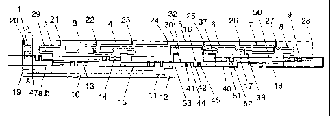
Figures 3a to 3c are three plan views (width reduced 1 /3 of length reduction)
of a
10-port device for an antenna beam-forming network with integrated tuneable
multi-.
channel phase shifter, with the movable dielectric bars in three different
positions;.
Figure 4 is a cross-section taken along a Line A-A in Figure 3a;
Figure 5 is a cross-section taken along a fine B-B in Figure 3b;
Figure 6 is an enlarged plan view (width reduced 1 /3 of length reduction) of
the right
hand side of the device of Figure 3b;
Figure 7 is a graph showing the variation in permittivity sr of the movable
dielectric
bars 47a and 47b taken along a portion of feedline 16;
Figure 8 is a graph showing the variation in permittivity s~ of the movable
dielectric
bars 47a and 47b taken along a portion of feedline 17;
Figure 9 is a schematic plan view of a segment of an alternative movable
dielectric
bar;
Figures 10a to 10c are three plan views (width reduced %z of length reduction)
of a
_5-port device for an antenna beam-forming network with integrated tuneable
multi-
channel phase shifter, with the movable dielectric bars in three different
positions;
Figure 1 1 is a cross-section taken along a line C-C in Figure 10a;
Figure 12 is a cross-section taken along a fine D-D in Figure 10c;
Figure 13 is a schematic plan view (width reduced by %i of length reduction)
of the
movable dielectric bar;
Figure 14 is a schematic plan view of a 3-port device with a stripline formed
with
stubs;
Figure 15 is a schematic plan view of a 3-port device with a stripline formed
as
meander line; and
Figure 16 is a cross section of a device as shown in Figure 10 with an
asymmetrical
stripline arrangement.
The preferred arrangements described below provide a tuneable multi-channel
phase
shifter integrated with a beam-forming network for a linear antenna array. In
order to
control the beam direction and beam shape of this antenna array we need to
provide
certain phase relations between the radiating elements. For subsequent control
and
changing the beam direction these phase relations should be varied in a
specific
CA 02457913 2004-02-18
WO 03/019723 PCT/NZ02/00164
8
manner. The beam-forming network also includes circuit-matching elements to
minimise signal reflection and maximise the emitted fields.
A 10-port feedline network with integrated phase shifter for a phased array
antenna
is shown in Figures 3 to 6. Conductor strips 1 to 18 form a feedline network
(the
dotted area in Figure 3). These conductor strips can be fabricated from
conducting
sheets !e.g. brass or copper) or PCB laminate by for example etching,
stamping, or
laser cutting. It should be noted that, for the purposes of clarity, the width
dimension of the device has been reduced by 1 /3 of the length reduction in
the
representation of Figures 3a-3c. As a result the view of the feedline is
somewhat
distorted in places.
As shown in Figures 4 and 5, the feedline network 1 to 18 is positioned
between
fixed dielectric blocks 43a, 43b, 46a, and 46b, and movable dielectric bars
47a and
47b. The whole assembly is enclosed in a conducting case, made of metal blocks
48a and 48b. The whole assembly forms a dielectric loaded strip-line
arrangement.
The pair of sliding dielectric bars 47a and 47b is housed between the metal
blocks
48a and 48b, in the space between the fixed dielectric blocks 43a, 43b, 46a,
and
46b. For clarity the contour of the upper bar 47a is outlined by a bold line
in the
three plan views of Figure 3. The bar 47a is shown in three different
positions in
Figures 3a, 1 b, and 1 c. The lower bar 47b has an identical profile to the
upper bar
47a. The bar profiles are formed by cutting portions of material from a single
piece
of dielectric material.
Figure 4 shows a cross section along line A-A in Figure 3a, where the bars 47a
and
47b have no off-cuts and entirely fill the space between the metal blocks 48a,
48b
and the dielectric blocks 43a, 43b, 46a, and 46b. Figure 5 shows a cross
section
taken along line B-B in Figure 3b, where the bars 47a and 47b have off-cuts
49a and
49b and partially fill the space between the metal blocks 48a, 48b and the
dielectric
blocks 43a, 43b, 46a, and 46b. All off-cuts in the bars 47a and 47b have well
defined locations and dimensions, which depend on the desired phase and power
CA 02457913 2004-02-18
WO 03/019723 PCT/NZ02/00164
9
relations at ports 20 to 28. Simultaneously, the off-cuts serve as circuit-
matching
transformers for the feedline network.
The bars 47a and 47b can be continuously moved along their length to provide a
desired phase shift. The movement of bars 47a and 47b provides simultaneous
adjustment of the phase shift at al) ports 20 to 28, The locations and
dimensions of
the off-cuts are chosen so that the movement of bars 47a and 47b within
certain
limits alters the phase relations between the ports 20-28 in a specified
manner
without changing the impedance matching at the input port 19.
To provide the desired division of power at each junction of the feedline
network,
circuit-matching transformers are integrated into the feedline network. An
example
of such circuit-matching elements is sections 1 1 and 12 near. junction 33 and
section
29 in strip conductor 2. Here the circuit matching is achieved by varying the
width
of the feedline section. The length and width of these circuit-matching
sections 1 1
and 12 is selected to minimise signal reflection at the junction 33. In a
preferred
arrangement the sections 1 1 and 12 both have lengths of approximately ~,\4
(where 7~
is the wavelength in the feedline corresponding to the centre of the intended
frequency band). These types of circuit-matching transformers will be referred
to
below as fixed transformers.
Another example of a circuit-matching element in this device is shown in
Figure 6.
Off-cut 52 and projection 51 on the moveable dielectric bar serve as an
impedance
matching transformer for the feedline segment 17 between junctions 37 and 38.
This
transformer matches the wave impedances between the part of stripline 17 where
it
crosses the left edge of projection 51, and the part of stripline 17 where it
crosses
the right edge of off-cut 52. This type of circuit-matching transformer will
be
referred to below as a moveable transformer. The length of the feedline
between
junction 38 and the right edge of off-cut 52 as well as the length of the
feedline
between junction 37 and the left edge of projection 51 vary with movement of
the
bars 47a, 47b. However the sum of the two lengths remains constant, regardless
of
the position of the bars 47a and 47b (within their working range), thus
maintaining
proper matching.
CA 02457913 2004-02-18
WO 03/019723 PCT/NZ02/00164
All of the movable and fixed transformers in the device decrease the wave
impedance
along the feedline network in the output direction. Therefore the steps in
width-
variation in the fixed transformers are smaller, and the lengths of the fixed
transformers are shorter, when compared with a similar device having no
moveable
transformers. The reduced length of the fixed transformers enables greater
movement of the moveable bars along a length of stripline with uniform width,
thus
allowing more phase shift. The smaller steps in width variation in the fixed
transformers result in lower return loss.
An alternative type of moveable transformer is positioned between junctions 33
and
37 (Figure 6). The transformer is similar to the moveable transformer between
junctions 37 and 38, but in this case is formed by two projections 41, 42 and
two
off-cuts 44, 45.
The moveable transformers act as cascaded impedance transformers ~as shown in
Figures 7 and 8 which illustrate variation of E~ along the feedlines adjacent
to the cut-
outslprojections 41, 42, 44, 45, 51 and 52.
The pattern of the strip conductors in Figure 3 serves as a power distribution
network
for antenna radiating/receiving elements (not shown) connected to ports 20 to
28.
The conductor pattern contains multiple splitters and circuit-matching
elements.
Thus the device can deliver an incoming signal from common port 19 to the
ports 20
to 28 with specified phase and magnitude distribution (transmit mode). Also,
the.
device can combine al) incoming signals from ports 20 to 28 to the common port
19,
with a predefined phase and amplitude relationship between the incoming
signals
(receive mode).
An alternative topology for the movable dielectric bars 47a and 47b is shown
in
Figure 9. In Figure 9, the off-cuts of the bars 47a and 47b are filled with a
dielectric
material 80 of different permittivity~to the bar material, for instance
polymethacrylimite.
CA 02457913 2004-02-18
WO 03/019723 PCT/NZ02/00164
11
A 5-port feedline network with an integrated multi-channel phase shifter for a
phased
array antenna is shown in Figures 10 to 13. The cross section is in principle
is
similar to the one for the 10-port device, as shown in Figures 4 and 5.
However, in
contrast to the layout of the 10-port device, input port 60 is positioned in
line with
output ports 61 to 64.
Conductor strips (shown as a dotted area in Figure 10) form the conductor
pattern
of the feedline network. These conductor strips can be fabricated from
conducting
sheets (e.g. brass or copper) or PCB laminate by for example etching,
stamping, or
laser cutting. As shown in Figures 1 1 and 12, the feedline network is
positioned
between fixed dielectric blocks 67a, and 67b, and movable dielectric bars 68a
and
68b. The whole assembly is enclosed in a conducting case, made of metal blocks
69a and 69b. The whole assembly forms a dielectric loaded strip-line
arrangement.
For clarity, the contour of the upper bar 68a is outlined by a bold line in
the three
.plan views of Figure 10. The bar 68a is shown in three different, positions
in Figures .,_ _ _ __
10a, 10b, and 10c. The lower bar 68b has an identical profile to the upper bar
68a.
The bar profiles are formed by removing portions of bar material, as shown in
Figure
13.
Figure 1 1 shows a cross section taken along line C-C in Figure 10a where the
moveable bars 68a, 68b have off-cuts 92a, 92b and partially fill the space
between
the metal blocks 69b, 69b next to fixed dielectric blocks 67a, 67b. Figure 12
shows
a device cross section taken along line D-D in Figure 10c where the bars 68a,
68b
have no off-cuts and entirely fill the space between the metal blocks 69a, 69b
next
to fixed dielectric blocks 67a, 67b. All off-cuts in the bars 68a and 68b have
well
defined locations and dimensions, which depend on the desired phase and power
distribution at ports 61 to 64. Simultaneously, the off-cuts serve as matching
transformers for the feedlines.
The bars 68a and 68b can be continuously moved along their length to provide a
desired phase shift. The movement of bars 68a and 68b provides simultaneous
adjustment of the phase shift at all ports 61 to 64. The locations and
dimensions of
CA 02457913 2004-02-18
WO 03/019723 PCT/NZ02/00164
12
the off-cuts are chosen so that the movement of bars 68a and 68b within
certain
limits afters the phase relations between the ports 61 to 64 in a specified
manner and
provides suitable matching at the input port 60.
Alternatively, the off-cuts 90 to 93 shown in Figure 13 could be filled with a
dielectric material of different permittivity to the bar material. Alternative
topologies
for the bars 68a and 68b are described in the section with the 10-port device
description.
To provide the desired division of power at each junction of the strip
conductor,
circuit-matching transformers are integrated into the distribution network
formed by
the strip conductors in Figure 10. Examples of such fixed circuit-matching
elements
are sections 65 and 66 near junction 69, sections 72 and 73 near junction 70,
and
sections 74 and 75 near junction 71. Here the circuit matching is achieved by
varying the dimensions of the feedline section. The length and width of these
circuit-
matching sections_ 65, 66 and 72 ,to 75 is selected_to_ minimise signal
reflection at the
junctions 69 to 71.The off-cuts 90 to 93 in the dielectric bar 68a move only
along a
uniform portion of the feedline network.
The off-cuts 90 and 92 change the phase shift between outputs 61 to 64 when
the
dielectric bar 68a moves. The off-cuts 91 and 93 are the moveable transformers
decreasing the wave impedance in the output direction from input 60 to outputs
61
to 64. In order to have equal wave impedances at the input and all four
outputs, the
transformers of the 5-port device must decrease the wave impedance along the
paths
from the input to each output 61 to 64 by a factor of 1 /4.' The fixed and
moveable
transformers of the 5-port device shown in Figure 10 facilitate this decrease
in the
following manner. The sections 65 and 66 decrease the wave impedance to 3/4,
the
sections 72 and 73 to 10/16, the off-cuts 91 to 2/3, and the off-cuts 93 to
4/5 of
the values at the beginning of each section.
It is possible to increase the phase shift per unit of bar-movement by
changing the
layout of the feedline network and creating a delay fine. This delay line may
be
formed with short stubs (shown in Figure 14) or arranged in a meander pattern
CA 02457913 2004-02-18
WO 03/019723 PCT/NZ02/00164
13
(shown in Figure 15). The arrangements shown in Figures 14 and 15 result in a
non-
linear dependence of phase shift and bar position, still suitable for antennas
with
variable downtilt.
Thus the proposed device provides a beam-forming network for an antenna array
with electrically controllable radiation pattern, beam shape and direction.
The new
arrangement integrates the adjustable multi-channel phase shifter and power
distribution circuitry into a single stripiine package.
The feedline network, as described above for the 5-port and 10-port device is
symmetrical and contains two ground-planes 69a and 69b and two moveable
dielectric bars 68a and 68b. It is possible to use a different arrangement
containing
one ground plane 69b and one dielectric moveable bar 68b, as shown in Figure
16,
to realise a multi-channel phase shifter. This non-symmetrical arrangement
provides
a simpler design, although it yields less phase shift and higher insertion
loss than in a
__symmetrical arrangement.
Principles of Operation
The operation of the feedline network 2 of the 10-port device will now be
described
with reference to the transmit.mode of the antenna. However it will be
appreciated
that the antenna may also work in receive mode, or simultaneously in transmit
mode
and receive mode.
Phase Relationships:
An input signal on common fine 10 (Fig.3) propagates via impedance-matching
transformers 1 1 and 12 to junction 33. At junction 33 the signal is split and
it
propagates via subsequent feedlines and a series of splitters to nine ports 20
to 28.
Radiating elements (not shown) are connected, in use, to the nine ports 20 to
28.
The amplitude and phase relationships between the signals at the nine ports 20
to 28
determine the beam shape and direction in which the beam is emitted by the
antenna. The angle between the beam direction and horizon ~is conventionally
known
CA 02457913 2004-02-18
WO 03/019723 PCT/NZ02/00164
14
as the angle of 'downtilt'. The beam can be directed to the maximum 'downtilt'
direction by creating the maximum phase shift ~P between each pair of
neighbouring
ports.
Referring now to Figure 6, feedline 5 leads from junction 33 to central port
24.
Feedline 5, branching off from sputter 33, is formed by folded lengths of
stripline .
with an impedance matching step 32. Regardless of the position of the bars 47a
and
47b, there is no change in permittivity along the path of the strip conductor
between
junction 33 and port 24 (as can be seen in Figures 3a, b and c). Therefore,
the
electrical length of the feedline between junction 33 and central port 24
remains
constant at all positions of the dielectric bars.
The dimensions of this device are chosen in a way that with the bars 47a and
47b
set in the extreme left position shown in Figure 3b, the ports 20 to 28 are in
phase
(that is, OP is zero). Moving the bars 47a and 47b to the right simultaneously
_ chang.e_s the _e_lectrical length of certain .parts of th_.e. feed network
between the bars
47a and 47b. For feedline 16 between junctions 33 and 37 in Figure 6, moving
the
bars 47a and 47b to the right decreases the length of feedline 16 covered by
projection 40 and simultaneously increases the open length of feedline 16
between
junction 33 and the left edge of projection 41 . With the permittivity s~ of
the
projections being higher than the permittivity of the off-cuts, as shown in
Figure 7,
moving bars 47a and 47b to the right will therefore decrease the length
feedline 16
with higher s, and increase the length .with lower E~. As a result this will
decrease the
phase difference 4P between junctions 33 and 37.
For the feedline 17 between junctions 37 and 38, moving the bars 47a and 47b
to
the right decreases the length of this feedune covered by projection 50, and
siri~ultaneously increases the length of this feedline between junction 37 and
the left
edge of projection 51.
The dimensions of the device are also chosen so that regardless of the
positions of
bars 47a and 47b (within their working range) there is a phase shift dP/2
between
each pair of neighbouring ports. With the bars in the middle position (Figure
3a) the
CA 02457913 2004-02-18
WO 03/019723 PCT/NZ02/00164
phase shift relative to port 24 is -2 *~P degree at left-hand port 20, and + 2
~~P
degree at right-hand port 28. With the bars in the extreme right position
(Figure 3c)
the phase shifts relative to port 24 are -4~OP degree at left-hand port 20,
and
+4'''dP degree at right-hand port 28.
The amount of phase shift ~P is determined by the permittivity of the material
used
for bars 47a and 47b, and the off-cut shape. The permittivity of the
dielectric
materials used affects the phase velocity of the signals travelling in the
feedline
network. Specifically, the higher the permittivity, the lower the phase
velocity or
longer the electrical length of transmission fine. Thus, by varying the length
of
dielectric bar sections that overlap (as viewed from the perspective of Figure
3) the
strip conductors of the feedlines, it is possible to control the phase shift
between the
signal at the ports 20 to 28. A dielectric material "Styrene" or polypropylene
is used
for fabricating the moveable dielectric bars 47a, 47b.
The layout of the feedline network, and the locations and sizes of the off-
cuts in bars
47a and 47b can be altered to obtain different phase relationships between the
ports
to 28.
The operation of the feedline network 2 of the 5-port device will now be
described
with reference to the~transmit mode of the antenna. However it will be
appreciated
that the antenna may also work in receive mode, or simultaneously in transmit
mode
and receive mode.
An input signal on feedline 60 (Fig.10) propagates via impedance-matching
transformers 65 and 66 to a junction 69. From the junction 69 the signah is
fed via
junction 70 to ports 61 and 62, and via junction 71 to ports 63 and 64.
Radiating
elements (not shown) are connected, in use, to the four ports 61 to 64. The
phase
relationship between the signals at the four ports 61 to 64 determines the
beam
shape and direction in which the beam is emitted by the antenna.
The position of the dielectric bars 68a and 68b controls the phase
relationship
between the ports 61 to 64. The following refers to a device with the off cuts
of
CA 02457913 2004-02-18
WO 03/019723 PCT/NZ02/00164
16
bars 68a and 68b shaped as shown in figures 10 and 13. The location and size
of
the off-cuts is chosen to obtain phase relationships as described below.
With the bars 68a and 68b set in the middle position, shown in Figure 10b, the
ports
61 to 64 have specified phase relationships. Moving for example the bars 68a
and
68b to the left changes simultaneously the electrical length of certain parts
of the
feedline network between the bars 68a and 68b. For example, when moving bars
68a and 68b from the middle position (Figure 10b) to the extreme left (Figure
10a)
the length of the feedline between junction 69 and the left edge of off-cut 90
increases, and the length of the feedline between the left edge of 91 and
junction 70
decreases simultaneously. The off-cuts 92 have a smaller width than off-cut 90
to
change the variable phase shift between outputs 61 and 62 by only half the
amount
than between outputs 61 and 63. With the moving bars 68a and 68b at the
extreme
left position (Figure .1 Oa) the phase shift relative to port 61 is - ~P at
port 62, - 2 SOP
at port 63 and - 3~4P at port 64.
The amount of phase shift ~P is determined by the permittivity of the material
used
for bars 68a and 68b, and the off-cut shape. The permittivity of dielectric
materials
used affects the phase velocity of the signals travelling in the feedline
network.
Specifically, the higher the permittivity, the lower the phase velocity or
longer
electrical length of transmission line. Thus, by varying the length of
dielectric bar
sections that overlap (as viewed from the perspective of Figure 1 ) the strip
conductors of the feedlines, it is possible to control the phase shift between
the
signal at the ports 20 to 28. A dielectric material "Styrene" is used for
fabricating
moveable dielectric bars 68a and 68b.
The offcuts in the dielectric bars may be removed by a stamping operation, or
by
directing a narrow high pressure stream of fluid onto the material to be
removed.