Note: Descriptions are shown in the official language in which they were submitted.
CA 02458017 2004-02-18
1
TERMINAL STRUCTURE OF DIRECT ELECTRIC CURRENT
SUPERCONDUCTING CABLE AND
DC SUPERCONDUCTING CABLE LINE
BACKGROUND OF THE INVENTION
Field of the Invention
The present invention relates to the terminal structure of a direct
electric current (DC) superconducting cable and to a DC superconducting cable
line.
Description of the Related Art
The superconductor of a superconducting cable is generally constituted
by a superconducting layer which is formed by spirally winding
superconducting wires around a core material (hereinafter called a "former").
When the superconducting cable is used as a direct electric current cable,
soldering is generally performed for connecting superconductors together or
connecting the end of a superconductor with a wire consisting of a normal
conductor (for example, refer to Japanese Patent Application Publication No.
10-228933). Some of superconducting cables have a multilayer structure
superconductor consisting of a plurality of superconducting layers (for
example,
see Fig. 3 of Japanese Patent Application Publication No. 10-228933). In this
case, as shown in Fig. 3 of the 10-228933 gazette, soldering is done
simultaneously such that the ends of all superconducting layers conduct to
each other.
CA 02458017 2004-02-18
2
In a DC power transmission and distribution system which is
constituted by a plurality of power supplies and loads, a plurality of cables
are
connected to the respective power supplies so as to form a plurality of
circuits,
which results in increase in the number of cables to be used. In this case, it
is
possible to increase the amount of electric current and to decrease loss by
using
superconducting cables. However, a number of cables must be used according to
the number of the power supplies, and the space for arranging the cable
distribution line is necessary.
SUMMARY OF THE INVENTION
An object of the present invention is to provide a terminal structure of a
direct electric current superconducting cable and a direct electric current
superconducting cable line, in which a single superconducting cable is made
possible to transmit electric power of a plurality of circuits so that the
transmission of increased electric current, the minimization of needed space,
and the decrease of transmission loss can be achieved.
In order to achieve the above object, the direct electric current
superconducting cable of the present invention has a core material (i.e.,
former),
a plurality of superconducting layers, and outgoing conductors made of a
normal conductor material, wherein the superconducting layers are provided
around the former in a manner such that the end portions of, the
superconducting layers are exposed step-by-step from an outer layer to an
inner layer, and the outgoing conductors are individually connected with the
CA 02458017 2004-02-18
3
respective stepwise exposed portions of the superconducting layers.
The outgoing conductors may be connected individually with the exposed
end of each layer of the superconducting layers in a manner such that the
outgoing conductors are extended in a direction perpendicular to the axial
direction of the superconducting cable. One end of the outgoing conductors may
be connected with the exposed end of the superconducting layer such that the
outgoing conductors are extended therefrom along the axial direction of the
superconducting cable.
Moreover, an insulating fixing member may be provided so that the core
material and the outgoing conductors are held integrally. A return-current
conductor layer made of superconducting material may be provided outside the
electrical insulation layer, and an insulating protective layer may be
provided
thereon.
Thus, using the direct current superconducting cable terminal structure
of present invention, a direct electric current superconducting cable line,
which
has power supplies, loads and a superconducting cable for supplying electric
power from the power supplies to the loads, can be formed.
In such case, it is preferable that at least one end of the superconducting
cable have any of the terminal structures described above such that each
outgoing conductor is connected to each power supply or load.
Moreover, the above-mentioned direct electric current superconducting
cable line of present invention may be,equipped with a cutoff mechanism for
cutting-off the grounded superconducting layer from the corresponding power
CA 02458017 2010-11-23
4
supply and load when any superconducting layer of the superconducting cable
is grounded.
Also, layer-insulations provided in. the superconducting cable may be
afforded with the dielectric strength that enables the voltage of other
superconducting layers to be maintained when any layer of the
superconducting multiple layers is grounded.
According to an aspect of the present invention there is provided a
terminal structure of a direct electric current superconducting cable
comprising:
a core,
a plurality of superconducting layers provided over the core,
outgoing conductors made of a normal conductive material, wherein
the end portion of each of the superconducting layers is exposed in a step-by-
step manner from an outer layer to an inner layer, and the outgoing
conductors are individually connected with the exposed end portions of the
respective superconducting layers,
layer insulations for insulating between the superconducting layers,
and
an insulating fixing member for integrally supporting the core and the
outgoing conductors,
CA 02458017 2011-05-27
4a
wherein an electrical insulation layer, a return-current conductor
layer, and an insulating protective layer are provided in the enumerated
order over an outermost superconducting layer.
According to another aspect of the present invention there is provided
the direct electric current superconducting cable comprising power supplies,
loads and a superconducting cable for supplying electric power from the
power supplies to the loads, wherein at least one end of the superconducting
cable has a terminal structure as described herein, and each outgoing
conductor is connected with one of the power supplies or one of the loads.
BRIEF DESCRIPTION OF THE DRAWINGS
Figure 1 is a sectional view of a superconducting cable according to the
present invention.
Figure 2 is a sectional view showing the structure of a former and a
superconducting layer in the terminal portion of the cable core of a
superconducting cable according to the present invention.
Figure 3 is a schematic diagram showing a terminal structure of a
superconducting cable according to a first embodiment of the present
invention.
Figure 4 is a schematic diagram showing a terminal structure of a
CA 02458017 2011-05-27
4b
superconducting cable according to a second embodiment of the present
invention.
Figure 5 is a schematic diagram showing a cable line which adopts the
terminal structure of a superconducting cable according to the present
invention.
CA 02458017 2004-02-18
DESCRIPTION OF THE PREFERRED EMBODIMENTS
Hereinafter, a detailed explanation of the present invention is given.
In the drawings, the same mark is put to the identical elements and
their explanation will not be repeated. The ratio of sizes in the drawings may
5 not always agree with the description in the specification. Figure 1 is a
sectional view of a superconducting cable according to the present invention,
and Fig_ 2 shows the terminal structure of conductor part in a cable core of
the
superconducting cable. Figure 3 and Fig. 4 schematically illustrate the
terminal structure of the conductor part of the superconducting cable core to
which the outgoing conductors are connected. Figure 5 is a schematic diagram
showing the structure of a cable line using a superconducting cable, and in
the
figure the illustration is given with respect to the structure of a cable
core.
[The whole structure of a superconducting cable]
A superconducting cable may have a single core or three stranded cores.
The superconducting cable is housed in a thermal insulation pipe in which a
coolant is to be filled so as to obtain cryogenic temperature. The thermal
insulation pipe preferably has a double pipe structure consisting of a
corrugated inner pipe and outer pipe, each made of stainless steel, for
example,
and the space between these inner and outer pipes is kept in vacuum condition.
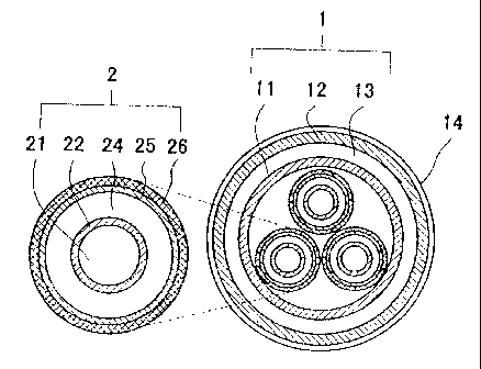
Figure 1 is a superconducting cable according to one embodiment of the
present invention, in which three stranded cable cores 2 are housed inside a
thermal insulation pipe 1.
CA 02458017 2004-02-18
6
[Thermal insulation pipe ]
The thermal insulation pipe 1 has a double-pipe structure consisting of
an inner pipe 11 and outer pipe 12, and a thermal insulating layer 13 is
formed
between the inner pipe 11 and the outer pipe 12. A so-called super insulation,
which consists of a stack of laminated plastic reticulate body and metallic
foil,
is arranged in the thermal insulating layer 13. A coolant such as liquid-
nitrogen is filled inside the inner pipe 11. An anticorrosion layer 14 made of
polyvinyl chloride or the like may be provided, according to need, around the
outer periphery of the thermal insulation pipe 1.
[ Cable core ]
Each of the cable cores 2, which are to be housed in the thermal
insulation pipe 1, is provided with, in the enumerated order from the center
as
shown in Fig. 1 and Fig. 5, a former 21 which is to function as a core
material, a
superconducting layer 22 which is to function as a superconductor, a layer
insulation 23 (shown in Fig. 5), an electrical insulation layer 24, a return-
current conductor layer 25, and an insulating protective layer 26 having both
functions of insulation and mechanical protection.
< Former >
The former 21 may be a solid made of stranded metal wires or a hollow
body made of a metallic pipe. In the case of a hollow former, the inside
thereof
can also be used as a path for a coolant. A solid former is made of stranded
copper wires, for example. The copper wires need not be provided with an
insulation covering because the superconducting cable of the present invention
CA 02458017 2004-02-18
7
is used for direct current.
< Superconducting layer >
The superconducting layer 22 is preferably made of tapes consisting of
oxide high Tc superconductor, such as a Bi-based superconductor, which is
covered with a silver sheath. These tapes constitute a conductor by being
wound around the former 21 in multiple layers.
< Layer insulation >
A layer insulation 23 in the superconducting cable is provided by
winding a kraft paper around each superconducting layer 22 so that each layer
of the multiple superconducting layers 22 can be independent of other
superconducting layers 22. The thickness of the layer insulation 23 is
designed
to be sufficiently thick to have the dielectric strength that enables the
voltage
of the other superconducting layers can be maintained when any
superconducting layer is grounded partially. Thus, a large electric current
flowing through such grounded superconducting layer can be cut off so that it
may not influence on the power transmission of other superconducting layers.
< Electrical insulation layer >
It is preferable to provide a superconducting cable with an electrical
insulation layer such that the outer side of the outermost superconducting
layer is covered with the electrical insulation layer. The electrical
insulation
layer 24 is formed by winding a compound tape consisting of a laminated
plastic film (e.g., polypropylene) and kraft paper, or example, around the
outer
periphery of the outermost superconducting layer 22.
CA 02458017 2004-02-18
8
< Return-current conductor layer >
The return-current conductor layer 25 is formed by winding
superconducting tapes around the outer side of the electrical insulation layer
24. This return-current conductor layer 25 allows an electric current to flow
in
the direction opposite the direction of the electric current flowing through
the
superconducting layer 22 in a cable line described later so that a magnetic
field
may not let out to the outside of the cable. Moreover, the insulating
protective
layer 26, which also functions as protection, is provided around the outer
side
of the return-current conductor layer 25.
[ Cable terminal structure ]
Hereinafter, an explanation is given about a cable terminal structure in
the case of 4 superconducting layers 22. Figure 2 shows only a former 21 and
superconducting layers 22 at the end portion of cable core 2. The end of each
superconducting layer 22 is individually connected, at the terminal portion of
the cable, with a corresponding outgoing conductor 3 which is composed of a
normal conductive material.
< Terminal structure of the cable core >
The former 21 protrudes from the end of the superconducting layers 22.
The superconducting layers 22 are structured such that the end portion thereof
is exposed step-by-step from an inner layer to an outer layer. More
specifically,
at the end portion of the cable, the electrical insulation layer 24 formed on
the
outermost superconducting layer 22, the return-current conductor layer 25,
and the insulating protective layer 26 are removed at a given length,
CA 02458017 2004-02-18
9
respectively.
Thus, at the exposed portion of the outermost superconducting layer 22
about which the electrical insulation layer 24 is removed, the outermost
superconducting layer 22 and the layer insulation 23 directly under it are
removed such that the superconducting layer 22 immediately thereunder is
exposed protruding at a given length from the end faces of the electrical
insulation layer 24 and other members which have partly been removed.
Subsequently, at the exposed portion of the next superconducting layer
(i.e., the second superconducting layer adjacent to the outermost layer which
has partly been removed), the above-mentioned next superconducting layer
and the layer insulation immediately thereunder are removed partially such
that the superconducting layer adjacently thereunder is exposed at a given
length from the end face of such partly removed outermost superconducting
layer. In this manner, the end portion of each superconducting layer is
exposed
stepwise at given length by repeating the process to remove the end portions
of
a superconducting layer and the layer insulation directly under it in the
order
from an outer layer to an inner layer to the innermost superconducting layer
(i.e., the fourth superconducting layer).
< Structure of the outgoing conductors >
The structure of outgoing conductors 3 will be described hereunder about
first and second embodiments of the present invention as shown in Fig. 3 and
Fig. 4, respectively. In each embodiment, the outgoing conductors 3 composed
of a normal conductive material such as copper or aluminum are connected by
CA 02458017 2004-02-18
soldering individually with the exposed end of the respective corresponding
superconducting layers 22.
In the first embodiment shown in Fig. 3, a plurality of outgoing
conductors 31 (3) are formed, and an end of each outgoing conductor 31 is
5 connected individually with the exposed end of a corresponding
superconducting layer 22. Then, the other end portion of each outgoing
conductor is extended from the exposed portion of the respective
superconducting layers 22 at a right angle relative to an axial direction of
the
superconducting cable. In this case, the respective outgoing conductors 31 are
10 extended in parallel as shown in Fig. 3.
The outgoing conductors 32 (3) of the second embodiment shown in Fig. 4
are composed of a plurality of outgoing conductors 32 each having a tubular
shape (or a tubular shape divided in half circle) of a different dimension. An
end of the outgoing conductors 32, are connected with the exposed end portion
of
the corresponding superconducting layers 22 in a manner such that the tubular
bodies are disposed concentrically one over the other. Then, the other end of
the
outgoing conductors 32 are extended along the axial direction of the cable.
The outgoing conductors 32 are connected with the exposed portion of the
superconducting layers 22 such that an inner superconducting layer is
connected with an outgoing conductor having a smaller diameter step by step
in the order of a smaller one to a larger one.
For extending the outgoing conductors along the axial direction of the
superconducting cable, an end of the outgoing conductor made of wires instead
CA 02458017 2004-02-18
11
of a tubular body may be individually connected with the exposed end of each
superconducting layer.
Moreover, the end of each outgoing conductor 32 is exposed stepwise so
that the outer surface thereof is exposed step by step from an inner one to
outer
one. Such structure makes it possible to easily connect other conductors with
the ends of the outgoing conductors 32.
< Structure for supporting the former and outgoing conductors >
The former 21 and outgoing conductors 3 are integrally supported by an
insulating fixing member 4. The insulating fixing member 4 is made of an
insulative resin material and is structured so as to electrically insulate
between the outgoing conductors 3, between an outgoing conductor 3 and the
other superconducting layers 22 but the superconducting layer 22 with which
the outgoing conductor 3 is connected, and between the former 21 and the
outgoing conductors 3. The terminal end of the superconducting cable can be
fixed by supporting the former 21 and the outgoing conductors 3 with the
insulating fixing member 4. In addition, supporting the core material and the
outgoing conductors with the insulating fixing member improves the strength
of the superconducting cable terminal structure. Preferably, the insulating
fixing member has a structure to insulate between the outgoing conductors,
and between the outgoing conductors and the superconducting layers with
which no outgoing conductors are connected.
[ Structure of a cable line ]
When a plurality of power supplies are arranged on the side of an end of
CA 02458017 2004-02-18
12
the superconducting cable, each power supply is connected with one of the
outgoing conductors which are connected individually with the ends of the
respective superconducting layers on that side. Also, when a plurality of
loads
are arranged on the side of the other end of the superconducting cable, each
load is connected with one of the outgoing conductors which are connected
individually with the ends of the superconducting layers on that side.
In the case where a plurality of power supplies are arranged on the side
of an end of the superconducting cable, and loads, which correspond to the
respective power supplies, are arranged on the side of the other end of the
superconducting cable, both ends of each superconducting layer are connected
individually with the respective outgoing conductors, and a power supply and a
corresponding load are connected with one superconducting layer through the
outgoing conductors.
For example, in a case where the superconducting cable has a core
material, a plurality of superconducting layers, an electrical insulation
layer
provided outside the outermost superconducting layer, a return-current
conductor layer provided outside the electrical insulation layer, and an
insulating protective layer, the outgoing conductors, which are connected
individually with the ends of the respective superconducting layers, are
extended to the outside of a superconducting cable. Then, power supplies are
connected individually with the respective outgoing conductors which are
connected with the end portion of the superconducting cable. Also, loads are :
connected individually with the respective outgoing conductors which are
CA 02458017 2004-02-18
13
connected with the other end portion of the superconducting cable. Then, each
power supply and each load are connected through the return-current
conductor layer of the superconducting cable.
In this case, it is possible to prevent a magnetic field from leafing out to
the outside of the cable because an electric current flows in the return-
current
conductor layer in the opposite direction relative to the electric current
flowing
through a superconducting layer. Each power supply and each load share a
return-current conductor layer as the ground potential (common potential).
In a cable line, all of the voltages may be the same or may be different.
An explanation is given hereunder with reference to Fig. 5 about a
superconducting cable according to one embodiment of the present invention.
The superconducting cable line shown in Fig. 5 is an example in which one
cable core 2 is used.
In the cable line shown in Fig. 5, a plurality of power supplies 5 are
arranged on the side of an end of a cable core 2, and loads 6 are arranged on
the
side of the other end of the cable core such that each load corresponds to one
of
the power supplies 5. Both ends of each superconducting layer 22 of the cable
core 2 are connected individually with outgoing conductors 3, and each
outgoing conductor 3 is connected with a power supply 5 or load 6. Thus, one
power supply 5 is connected with one corresponding load through one
superconducting layer 22 and outgoing conductors 3 connected thereto. The
return-current conductor layer is connected through another conductor with all
power supplies 5 and all loads 6.
CA 02458017 2004-02-18
14
A closed loop circuit is constituted by using a superconducting layer 22 of
the cable core 2 and the return-current conductor layer 25. All of the voltage
to
be used in the closed loop circuits of the present embodiment can be the same
or different. In the cable line, cutoff mechanisms 7 are provided so that if a
superconducting layer 22 of the cable core 2 is grounded, it can be cut off
from
the power supply 5 and the load 6. Here, the words "a superconducting layer of
the superconducting cable is grounded" mean that a power supply or a load is
grounded for an inspection, a failure, or the like.
Preferably, the cutoff mechanisms are provided at both ends of the cable-
In such case, the superconducting layer which is grounded can be cut off from
the power supply and the load by using the cutoff mechanism. For example,
the cutoff mechanism maybe constituted such that voltmeters or ammeters are
provided at both ends of the superconducting layers, and relays, which operate
based on the results of measurement by the voltmeters or the ammeters, are
provided. An electric fuse may be provided instead of the relay.
For example, the cutoff mechanisms 7 shown in Fig. 5 are constituted by
providing voltmeters (not illustrated) or ammeters (not illustrated) in the
outgoing conductors 3 which are connected with either ends of the
superconducting layers 22, and by providing relays 71 which operate according
to the results of measurement by the voltmeters or the ammeters. The
voltmeters measure voltage at both sides of the relays 71. The ammeters
measure an electric current at both sides of the relays 71. In the event that
a
superconducting layer is grounded, the grounded superconducting layer is cut
CA 02458017 2004-02-18
off from the power supply and the load by the cutoff mechanism 7 so that the
other superconducting layers are protected.
As described above, it is possible to constitute a plurality of circuits with
one cable core by using the terminal structure of the direct electric current
5 superconducting cable of the present invention and the structure of the
direct
electric current superconducting cable line. Also, the power transmission loss
can be reduced because a superconducting cable is used. Therefore, the cost
performance is excellent and the required space can be reduced. Moreover, it
is
possible to prevent a magnetic field from leaking out to the outside of the
cable
1 0 by providing a return-current conductor layer in which an electric current
is
caused to flow in the opposite direction relative to the electric current
flowing
through the superconducting layer.