Note: Descriptions are shown in the official language in which they were submitted.
CA 02458134 2004-02-19
- 1 -
NITRIDE SEMICONDUCTOR DEVICE
BACKGROUND OF THE INVENTION
1. Field of the Invention
The present invention relates to semiconductor devices
having micro-area (width) electrodes on nitride semiconductor
layers, and particularly to high-current-driven electronic
devices, such as laser diodes, high-power LEDs, FETs, and
high-frequency devices. Such semiconductor devices comprise,
for example, group III-V nitride semiconductors, such as GaN,
AIN, and InN, including their mixed crystals AlGaN, InGaN, and
AlInGa.
2. Description of the Related Art
Nitride semiconductor devices emit light having a wide
range of wavelengths from a relatively short-wavelength
ultraviolet region to a visible light region including that of
red light, and are widely used for semiconductor laser diodes
(LDs) and light emitting diodes (LEDs). Nitride semiconductor
devices have been developed for miniaturization, increased
lifetime, and enhanced power consumption, and have been
principally used in electronic apparatuses such as personal
computers and DVDs, medical equipment, processing machinery,
and light sources for optical fiber communication.
A typical nitride semiconductor device is a composite
including a buffer layer, an n-type contact layer, a crack-
free layer, an n-type cladding layer, an n-type light guide
layer, an active layer, a p-type electron confinement layer, a
CA 02458134 2004-02-19
- 2 -
p-type light guide layer, a p-type cladding layer, and a p-
type contact layer, in that order, on a sapphire substrate.
For an LED, it is not necessary to provide the light guide
layers or the like. The composite is provided with n and p
electrodes through which the active layer is energized to emit
light.
In the electrodes, portions establishing an ohmic contact
between the electrodes and respective semiconductor layers
play a key role, and are generally formed of a high-work-
function elemental metal or alloy in a single-layer or
multilayer form. Some metals can establish an ohmic contact
with a semiconductor layer by only depositing the metals on
the semiconductor layer. For example, a Pd/Pt/Au multilayer
film may be used as a p electrode. For an electrode material
that does not easily form an ohmic contact with the
semiconductor layer by only deposition, heat treatment allows
the electrode material to establish an ohmic contact. For
example, a Ni/Au multilayer film can be alloyed to be a
transparent p electrode functioning as an ohmic electrode by
heat treatment.
The n and p electrodes each have an extraction portion
(pad electrode) for bonding a wire. If the substrate is
insulative, pad electrodes are provided to both the n and p
electrodes because the n and p electrodes are disposed on the
same side of the substrate. Since the ohmic contact with an
n-type semiconductor layer is relatively easily established,
the ohmic electrode of an n electrode may double as the
extraction electrode. A metallized layer to be connected to
CA 02458134 2004-02-19
- 3 -
external electrodes, but not to wires, may be provided on the
extraction electrode so that the device can be mounted face
down.
In addition, an insulating layer is provided between the n
and p electrodes. The insulating layer may be formed by a
single-layer or multilayer oxide film. For an LD, the
insulating layer is also used as a functional film having
additional function, such as a current constriction film for
controlling a current-injection region or a reflective film
provided on the surface of a resonator.
These nitride semiconductor devices are disclosed in, for
example, Japanese Unexamined Patent Application Publication No.
2000-299528.
However, the surface of the above-described Ni/Au
electrode is liable to be damaged by heat treatment.
Consequently, the resistance at the interface between the
Ni/Au electrode and the pad electrode may be increased. If an
insulating layer is in contact with the Ni/Au electrode, the
insulating layer is degraded by heat treatment to reduce
adhesion to the electrode. The Pd/Pt/Au electrode does not
readily cause such a problem because the Pd/Pt/Au electrode is
not subjected to heat treatment. However, an increase in
device temperature during operation may degrade the
characteristics of the electrode, consequently increasing the
operating voltage disadvantageously. In addition, a thin
electrode or a wide electrode degrades adhesion or mechanical
strength, thus causing a problem during high-current operation.
ak 02458134 2009-06-26
- 4 -
SUMMARY OF THE INVENTION
In view of the above-described disadvantages, the
object of the present invention is to provide a nitride
semiconductor device exhibiting a low threshold current and
operating voltage and other superior characteristics which
includes electrodes achieving a low contact resistance with
a semiconductor layer and a low interface resistance between
a pad electrode and an ohmic electrode and having superior
adhesion to a semiconductor layer and an insulating layer.
Certain exemplary embodiments may provide a nitride
semiconductor device comprising: a semiconductor layer; a
first electrode for establishing an ohmic contact disposed
on the semiconductor layer, the first electrode including an
upper layer and a lower layer and being subjected to heat
treatment; and a second electrode formed on the first
electrode, the second electrode having a different shape
from a shape of the first electrode, the second electrode
further including an upper layer and a lower layer, wherein
the upper layer of the first electrode consist of an
elemental metal, a compound or alloy including at least one
of Pt, Pd, Rh, Ir, Ru and Os and the lower layer of the
second electrode consists of an elemental metal, a compound
or alloy including at least one of Pt, Pd, Rh, Ir, Ru and Os
and form a joint region joining the first electrode to the
second electrode and at least one of materials forming the
upper layer of the first electrode and at least one of
materials forming the lower layer of the second electrode
are the same.
Certain other exemplary embodiments may provide a
nitride semiconductor device comprising: a semiconductor
layer; a first electrode for establishing an ohmic contact
ak 02458134 2009-06-26
- 4a -
disposed on the semiconductor layer; a second electrode on
the first electrode, having a different shape from the shape
of the first electrode; and an insulating layer on the
surface of the semiconductor layer, wherein the surface of
the semiconductor layer on which the first electrode is
formed comprises an electrode formation region and an
insulating layer formation region, and the second electrode
is disposed on the electrode formation region and the
insulating layer formation region; wherein the first
electrode includes an upper layer and a lower layer, and the
second electrode further includes an upper layer and a lower
layer, wherein the upper layer of the first electrode and
the lower layer of the second electrode each consist of an
elemental metal, a compound or alloy including at least one
of Pt, Pd, Rh, Ir, Ru and Os and form a joint region joining
the first electrode to the second electrode.
Yet another exemplary embodiment may provide a nitride
semiconductor device comprising: a semiconductor layer; a
first electrode for establishing an ohmic contact disposed
on the semiconductor layer; a second electrode on the first
electrode, having a different shape from the shape of the
first electrode; and an insulating layer of the surface of
the semiconductor layer, wherein the insulating layer is
disposed between a) the first electrode and the second
electrode and b) the semiconductor layer; and wherein the
surface of the semiconductor layer on which the first
electrode is formed comprises an electrode formation region
and an insulating layer formation region, and the second
electrode is disposed on the electrode formation region and
the insulating layer formation region; wherein the first
electrode includes an upper layer and a lower layer, and the
second electrode further includes an upper layer and a lower
ak 02458134 2009-06-26
- 4b -
layer, wherein the upper layer of the first electrode and
the lower layer of the second electrode each comprise an
elemental metal, a compound or alloy including at least one
of Pt, Pd, Rh, Ir, Ru and Os and form a joint region joining
the first electrode to the second electrode.
Still certain other exemplary embodiments may provide a
nitride semiconductor device comprising: a semiconductor
layer; an insulating layer being disposed on a portion of a
surface of the semiconductor layer; a first electrode for
establishing an ohmic contact and being disposed on another
portion of the semiconductor layer; an adhesion layer being
disposed on at least a portion of the =first electrode; and a
second electrode having a different shape from a shape of
the first electrode; wherein at least a portion of the
insulating layer is disposed between the first electrode and
the semiconductor layer; and wherein the surface of the
semiconductor layer on which the first electrode is disposed
comprises an electrode formation region and an insulating
layer formation region, wherein the first electrode further
includes an upper layer and a lower layer, and the second
electrode further includes an upper layer and a lower layer,
wherein the upper layer of the first electrode and the lower
layer of the second electrode each comprises an elemental
metal, a compound or alloy including one of Pt, Pd, Rh, Ir,
Ru, and Os.
Still certain other exemplary embodiments may provide a
nitride semiconductor device comprising: a semiconductor
layer; an insulating layer being disposed on a portion of a
surface of the semiconductor layer; a first electrode for
establishing an ohmic contact and being disposed on another
portion of the semiconductor layer; an adhesion layer being
disposed on at least a portion of the first electrode; and a
ak 02458134 2009-06-26
- 4c -
second electrode having a different shape from a shape of
the first electrode; wherein at least a portion of the
insulating layer is disposed between the first electrode and
the semiconductor layer; wherein the surface of the
semiconductor layer on which the first electrode is disposed
comprises an electrode formation region and an insulating
layer formation region, wherein the first electrode further
includes an upper layer and a lower layer, and the second
electrode further includes an upper layer and a lower layer,
wherein the upper layer of the first electrode and the lower
layer of the second electrode each comprises an elemental
metal, a compound or alloy including one of Pt, Pd, Rh, Ir,
Ru, and Os, and wherein the adhesion layer is disposed
between the first electrode and the second electrode.
Still certain other exemplary embodiments may provide a
nitride semiconductor device comprising: a semiconductor
layer; an insulating layer being disposed on a first portion
of a surface of the semiconductor layer; a first electrode
for establishing an ohmic contact and being disposed on a
second portion of the surface of the semiconductor layer; a
second electrode having a different shape from a shape of
the first electrode; an adhesion layer being disposed so
that at least a portion of the adhesion layer is in contact
with the second electrode; wherein at least a portion of the
insulating layer is disposed between the first electrode and
the semiconductor layer; and wherein the surface of the
semiconductor layer on which the first electrode is disposed
comprises an electrode formation region and an insulating
layer formation region, wherein the first electrode further
includes an upper layer and a lower layer, and the second
electrode further includes an upper layer and a lower layer,
wherein the upper layer of the first electrode and the lower
ak 02458134 2009-06-26
- 4d -
layer of the second electrode each comprises an elemental
metal, a compound or alloy including one of Pt, Pd, Rh, Ir,
Ru, and Os.
Other embodiments provide a nitride semiconductor
device which includes a semiconductor layer, a first
electrode for establishing an ohmic contact disposed on the
semiconductor layer, and a second electrode on the first
electrode, having a different shape from the shape of the
first electrode. The first electrode includes an upper layer
and a lower layer and is subjected to heat treatment. The
second electrode also includes an upper layer and a lower
layer. The upper layer of the first electrode and the lower
layer of the second electrode are each formed of an element
of the platinum group and form a joint region joining the
first electrode to the second electrode. Thus, the
electrodes exhibit superior adhesion and low operating
voltage.
Other embodiments provide a nitride semiconductor
device which includes a semiconductor layer, a first
electrode for
ak 024.58134 2009-06-26
- 5 -
establishing an ohmic contact disposed on the semiconductor
layer, and a second electrode on the first electrode, having a
different shape from the shape of the first electrode. The
first electrode includes an upper layer and a lower layer and
is subjected to heat treatment. The second electrode also
includes an upper layer and a lower layer. The upper layer of
the first electrode and the lower layer of the second
electrode are formed of the same material and form a joint
region joining the first electrode to the second electrode.
Thus, the electrodes exhibit superior adhesion and low
operating voltage.
Other embodiments provide a nitride semiconductor device
comprising: a semiconductor layer; a first electrode for
establishing an ohmic contact disposed on the semiconductor
layer, the first electrode including an upper layer and a
lower layer and being subjected to heat treatment; and a
second electrode on the first electrode, having a different
shape from the shape of the first electrode, the second
electrode including an upper layer and a lower layer,wherein
the upper layer of the first electrode and the lower layer of
the second electrode each comprise an element of the platinum
group and form a joint region joining the first electrode to
Other embodiments provide a nitride semiconductor device
comprising:a semiconductor layer;a first electrode for
establishing an ohmic contact disposed on the semiconductor
ak 02458134 2009-06-26
A
- 6 -
layer, the first electrode including an upper layer and a
lower layer and being subjected to heat treatment; and a
second electrode on the first electrode, having a different
shape from the shape of the first electrode, the second
electrode including an upper layer and a lower layer,wherein
the upper layer of the first electrode and the lower layer of
the second electrode comprise the same material and form a
joint region joining the first electrode to the second
electrode.
Other embodiments provide a nitride semiconductor device
comprising: a semiconductor layer; a first electrode for
establishing an ohmic contact disposed on the semiconductor
layer; a second electrode on the first electrode, having a
different shape from the shape of the first electrode; and an
insulating layer on the surface of the semiconductor layer,
wherein the surface of the semiconductor layer on which the
first electrode is formed comprises an electrode formation
region and an insulating layer formation region, and the
second electrode overlies the electrode formation region and
the insulating layer formation region.
The lower layer of the first electrode may be formed of a
material alloyed by heat treatment. Since the material of the
lower layer of the first electrode is changed to one form or
another by heat treatment, the structure of the lower layer of
the first electrode is varied from that before heat treatment.
For example, a lower layer in a multilayer form may be changed
CA 02458134 2004-02-19
- 7 -
to an alloyed single-layer form by heat treatment without
maintaining the multilayer form. By forming the lower layer
of the first electrode, which is in contact with the
semiconductor layer, of a material alloyed by heat treatment,
the resulting first electrode exhibits superior adhesion to
the semiconductor layer in comparison with an electrode formed
by only deposition. Some semiconductor compositions or
electrode materials can lead to an ohmic contact without heat
treatment. However, a semiconductor device having low
internal and external quantum efficiencies may generate some
heat causing property changes during operation. Heat
treatment enhances the adhesion of the first electrode to the
semiconductor layer and prevents the characteristics from
being degraded by heat generated during device operation. In
addition, the joint region formed with the upper layer of the
first electrode and the lower layer of the second electrode,
=
comprising an element of the platinum group enhances the
adhesion between the first electrode and the second electrode.
Thus, extremely superior adhesion is established from the
semiconductor layer to the second electrode. Consequently,
the resulting device can exhibit low operating voltage, and
such superior reliability as not to easily degrade the
characteristics with time because of difficulty of increase in
voltage during high-power operation.
Even if the upper layer of the first electrode is formed
of a material other than the platinum group while the lower
layer of the first electrode is formed of the above-described
material alloyed by heat treatment, good adhesion can be
CA 02458134 2004-02-19
- 8 -
established as long as the upper layer of the first electrode
and the lower layer of the second electrode are formed of the
same elemental metal or highly conductive compound capable of
maintaining the characteristics stable. However, such a
material may not be used that allows the upper layer of the
first electrode to react with the lower layer by heat
treatment to alloy and produce an insulative oxide.
Thus, by forming the upper layer of the first electrode
and the lower layer of the second electrode of the same
elemental metal of the platinum group or the same alloy or
conductive oxide of the platinum group metals, the resulting
electrodes exhibit extremely low resistance, superior adhesion,
and such superior reliability as not to easily degrade the
characteristics with time.
The upper layer of the first electrode may be formed of an
elemental metal of the platinum group consisting of Pt, Pd, Rh,
Ir, Ru, and Os or an alloyed material essentially composed of
homologous elements in the platinum group, i.e., Ru-Os, Rh-Ir,
or Pd-Pt. These materials result in an upper layer of the
first electrode relatively stable to heat. Accordingly, the
upper layer of the first electrode is not easily alloyed with
the underlying lower layer even if the lower layer is formed
of a material alloyed by heat treatment. Although a reaction
occurs at the interface between the upper and lower layers of
the first electrode, it does not progress to the inside of the
layers and, thus, the interface is maintained stable. By
forming the upper layer of the first electrode and the lower
layer of the second electrode of the same material, the
CA 02458134 2004-02-19
- 9 -
resulting electrodes exhibit low resistance and stable
operating characteristics. In particular, an alloyed material,
not elemental metal, of the platinum group, which has been
alloyed by heat treatment, results in a hard layer because of
its higher bonding strength than that of the simply deposited
alloy. Also, the alloyed material of the upper layer does not
react with the alloyed material of the lower layer to form an
alloy. Thus, the layered structure including the upper layer
and the lower layer is maintained even after heat treatment.
= The surface of the upper layer of the first electrode is
generally liable to react with ambient air during heat
treatment because it is exposed. However, the above-described
layer of the platinum group does not easily react with the
ambient air, and particularly does not produce highly
insulative oxides. However, oxygen is probably adsorbed in
one form or another on the surface of the first electrode as
long as it is present. In particular, oxygen coordinates
around atoms of the platinum group element because of
catalysis of the element. This reaction is explained below.
Figs. 6A to 6C are schematic illustrations of a ridge
stripe and its vicinity of a nitride semiconductor laser
device including a p-type nitride semiconductor layer with the
ridge stripe, a first insulating layer 609 on both side
surfaces and at both sides of the ridge stripe, a first
electrode 605 on the upper surfaces from the ridge stripe to
the first insulating layer 609, and a second electrode 606 on
the first electrode 605. The first electrode 605 includes an
upper layer 605(a) and a lower layer 605(b). The second
CA 02458134 2004-02-19
- 10 -
electrode also includes an upper layer 606(a) and a lower
layer 606(b). The upper layer 605(a) of the first electrode
and the lower layer 606(b) of the second electrode form a
joint region 613. As shown in Fig. 6A, oxygen is adsorbed or
put on the upper surface of the upper layer 605(a) of the
first electrode, which is formed of a material of the platinum
group after heat treatment of the first electrode. Then, when
the second electrode is deposited by, for example, sputtering,
the platinum group material of the second electrode is brought
into contact with the surface of the first electrode at an
accelerated speed by, for example, sputtering. At this moment,
the platinum group material rejects the oxygen from coming
into the inside of the first electrode and induces the
formation of the joint region 613, as shown in Fig. 6B. Thus,
the upper layer 605(a) of the first electrode and the lower
layer 606(b) of the second electrode share a region to form
the joint region, as shown in Figs. 6B and 6C.
The following description explains why this reaction
proceeds. Although oxygen is adsorbed or put on the platinum
group material of the first electrode to temporarily bond to
each other stably as shown in Fig. 6A, the bond is so weak as
to be easily broken by external force. This temporary, weak
bond can be easily broken by impact when the platinum group
material is brought into contact with the upper surface of the
first electrode at a high speed by, for example, sputtering
for depositing the second electrode. In addition to
mechanical impact, such as sputtering, heat application can
break the bond.
CA 02458134 2004-02-19
- 11 -
The platinum group material present on the surface of the
first electrode becomes unstable or active after the oxygen is
rejected, due to the breakage of the bond. Thus, the second
electrode is deposited with the boundary between the first and
second electrodes collapsed, thereby forming the joint region
613 where the constituents of the first and second electrodes
are mixed. Specifically, there is no distinct boundary
between the first electrode, which has been heat-treated, and
the second electrode and the interface will appear to have
been formed by continuous deposition. If a stable oxide is
formed on the surface of the first electrode even though it
does not reach the inside, the bond of the oxide at the
surface is not easily broken by sputtering. In contrast, the
bond of oxygen simply put on the surface can be easily broken.
Thus, the platinum group materials of the upper layer of the
first electrode and the lower layer of the second electrode
can be bonded to each other by preparing an oxygen-absent
state or by collapsing the oxygen-present state by impact of
deposition.
The upper layer of the first electrode formed of one of
the above-listed materials has ductility and malleability.
Accordingly, the material of the second electrode incoming at
a high speed can easily enter the inside of the upper layer of
the first electrode. The upper layer of the first electrode
formed of an elemental metal of the platinum group or an
alloyed material essentially composed of homologous elements
in the platinum group, which have ductility and malleability
but does not easily produce oxides at the surface even by heat
CA 02458134 2004-02-19
- 12 -
treatment, makes it possible to establish the above-described
bond with the material of the lower layer of the second
electrode.
If the first electrode is formed of Au, which has the
highest malleability in metal elements, the first electrode
needs a lower layer formed of a metal element other than Au
because ohmic contact between nitride semiconductors and Au is
difficult to establish. In addition, since Au significantly
easily diffuses by heat treatment, an alloying reaction with
the underlying lower layer easily proceeds inside the layer
while oxygen is taken in from the outside. Consequently, the
Au initially present in the upper layer moves inward to reduce
the Au content in the upper layer or to expose the metal other
than Au of the lower layer, and an oxide can easily be
produced. Thus, the Au upper layer of the first electrode
disadvantageously causes an insulative oxide to be produced in
the interface with the second electrode to provide an
electrical barrier and to degrade the adhesion to the second
electrode. Operating characteristics are also negatively
affected. By providing the upper layer of the first electrode
of a platinum group material, the resulting electrodes exhibit
a low resistance.
An upper layer of the first electrode formed of an alloy
constituted of nonhomologous elements of the platinum group,
such as Pt-Ir, also facilitates the rejection of oxygen on the
surface of the upper layer by sputtering. Thus, the upper
layer of the first electrode can be bonded with the platinum
group material of the lower layer of the second electrode in a
CA 02458134 2004-02-19
- 13 -
state where oxygen is not easily present at the interface.
Unfortunately, this type of alloy is hard and less ductile and,
accordingly, the material of the second electrode incoming at
a high speed does not easily enter the inside of this alloy.
Consequently, the thickness of the resulting joint region
becomes small. Thus, the bonding strength (bonding area) is
reduced to some extent in comparison with ductile materials.
However, this alloy can produce a good adhesion to the upper
layer of the first electrode without any problems by forming
the lower layer of the second electrode of different types of
materials by simultaneous sputtering or the like.
In addition to the elemental metals of the platinum grope
and the above-described alloyed material comprising the
platinum group metals, the upper layer of the first electrode
may comprise a conductive compound containing a platinum group
element and oxygen, such as rhodium oxide, palladium oxide, or
ruthenium oxide. Although these materials are oxides, the
upper layer of the first electrode formed of these oxides
exhibits low resistance and superior adhesion to the second
electrode. A compound containing a platinum group element and
oxygen has a higher bonding strength with oxygen than that of
an oxide (oxide with a low bonding strength) formed on only
the surface of a platinum grope metal layer or a platinum
group alloy layer or a state where oxygen is adsorbed or put
on the surface. If an oxide of the platinum group metals is
used for the upper layer of the first electrode, therefore,
the joint region may be formed by other mechanisms apart from
the above-described mechanism in which the joint region is
CA 02458134 2004-02-19
- 14 -
formed of an elemental metal or alloy of the platinum group to
achieve a low resistance and a high adhesion.
Heat treatment for alloying an upper layer of the first
electrode formed of an oxide of the platinum group metals
causes a thermal reaction in the layer. This upper layer of
the first electrode probably maintains a stable interface with
the lower layer of the first electrode, as in the upper layer
formed of an elemental metal of the platinum group. However,
the vicinity of the upper surface of the upper layer of the
first electrode, which is in contact with the ambient air, is
in a different state. While the elemental metal of the
platinum group brings the surface into a stable state by
temporarily adsorbing oxygen, the compound of a platinum group
element and oxygen gradually varies the ratio of the oxygen to
the platinum group element between the vicinity of the surface
and internal region of the upper layer such that gradual
composition changes occur depending on the depth from the
surface of the first electrode. The composition of the
vicinity of the surface of the upper layer is gradually
changed to, for example, a platinum group element-rich form or
an oxygen-rich form depending on ambient conditions in heat
treatment. Thus, the initial composition that is stable just
after deposition is collapsed and, thereby, the surface of the
upper layer of the first electrode is activated. The
activated surface is bonded with the platinum group element of
the lower layer of the second electrode and, consequently,
does not form a substantial boundary. Thus, the resulting
electrodes exhibit a low resistance. This is unique to
CA 02458134 2004-02-19
- 15 -
conductive oxides of the platinum group metals, and may result
from catalysis.
In any case, by activating or semi-activating the upper
layer of the first electrode and tightly bonding with the
material of the lower layer of the second electrode when the
lower layer is deposited, a joint region with no substantial
interface state density or with gradually varied interface
state densities can be formed. This joint region can be
provided by forming an interface (contact area) of an
elemental metal of the platinum group, which is hard to
oxidize, or a conductive compound comprising a platinum group
element, capable of maintaining the conductivity even if
oxidized, between the first electrode and the second electrode.
Thus, the resulting electrodes exhibit extremely low
resistance and superior reliability.
The lower layer of the second electrode may comprise an
elemental metal of the platinum group or an alloy of the
platinum group metals. The lower layer comprising an alloy of
the platinum group metals is of a metal mixture film formed by
simultaneously depositing at least two platinum group metals,
but not of a film alloyed by heat treatment. The lower layer
of the second electrode is liable to be affected by a reaction
product produced on the surface of the first electrode by heat
treatment or impurities remaining in an apparatus for
depositing the second electrode, in the early stage of the
deposition.
If the first electrode and the second electrode, which
influence the operation region or waveguide region of the
CA 02458134 2004-02-19
- 16 -
device can be continuously formed without shifting among
devices, the occurrence of discontinuous interfaces resulting
from the shifting among devices can be prevented. However,
while the first electrode requires heat treatment in order to
establish an ohmic contact and to enhance the reliability of
the resulting device, the second electrode, which functions as
an extraction electrode, is subjected to no heat treatment or
to gentler heat treatment than that for the first electrode.
Thus these two electrodes often have different functions and
shapes. It is therefore preferable that the first electrode
and the second electrode be formed in separate production
steps. Accordingly, by forming the lower layer, which is
deposited in the early stage of the formation of the second
electrode after the shifting among devices, of an elemental
metal of the platinum group or an alloy of the platinum group
metals, the second electrode is prevented from reacting with
an impurities on the surface of the first electrode and
remaining components, such as oxygen, in the apparatus for
forming the second electrode. Thus increase in resistance of
the interface with the first electrode is prevented.
A lower layer of the second electrode formed a material
other than the above-listed materials, such as Ti, establishes
good adhesion to a Pt upper layer of the first electrode.
However, Ti immediately reacts with oxygen adsorbed or put on
the surface of the first electrode to form an oxide in the
early stage of the deposition due to ease of bonding to oxygen.
Consequently, the first electrode and the second electrode are
separated by oxygen or an oxide. It is undesirable to use Ti
CA 02458134 2004-02-19
- 17 -
for the lower layer of the second electrode because Titanium
oxides are insulative and increase the resistance of the
interface with the first electrode. A simply adhesive
material, such as Ti, prevents peeling of the second electrode
that causes increase in resistance, but does not prevent
production of an insulative mediation that also causes
increase in resistance.
By forming the upper layer of the first electrode and the
lower layer of the second electrode of the above-described
platinum group materials, a joint region can be provided which
contains an extremely small amount of oxygen or no oxide
increasing resistance between the first electrode and the
second electrode. The above-described platinum group
materials may be used either the upper layer of the first
electrode or the lower layer of the second electrode to
enhance the characteristics of the entirety of the first
electrode and the second electrode. However, by forming the
joint region between the first electrode and the second
electrode of these materials, the resulting electrodes exhibit
extremely superior characteristics. In particular, by forming
the upper layer of the first electrode and the lower layer of
the second electrode of the same material of the platinum
group, superior adhesion can be achieved. Most preferably,
the upper layer of the first electrode and the lower layer of
the second electrode are formed of Pt. Thus, the resulting
device can exhibit low operating voltage, and such superior
reliability as not to easily degrade characteristics with time
even in high-power operation.
CA 02458134 2004-02-19
- 18 -
The nitride semiconductor device may further include an
insulating layer on the surface of the semiconductor layer.
The second electrode overlies the first electrode and the
insulating layer. The first electrode is in contact with the
semiconductor layer, and the contact region defines a current-
conduction path. In order to efficiently inject current into
a waveguide region in an LD, or into a luminescent layer in an
LED, the position of the current-conduction path is controlled.
In this instance, the layout of the first electrode is not
controlled, but the insulating layer is formed on the surface
of the semiconductor layer to provide a non-conductive region
and then the first electrode is formed. Thus, the position of
the current-conduction path can be easily controlled. Then,
the second electrode is formed so as to overlie the first
electrode and the insulating layer. Thus, current is allowed
to flow efficiently to the first electrode.
The first electrode may extend in a stripe and the
insulating layer may be disposed at both sides of the stripe
of the first electrode. In an LD as shown in Fig. 1, an
insulating layer is provided at both sides of the stripe of
the first electrode and the second layer is disposed in such a
manner as to cover both the first electrode and the insulating
layer. Thus, the current-conduction path to the semiconductor
layer is disposed in a desired position. In an LED having
first electrodes arranged in a grid manner or a striped manner,
an insulating layer is provided on the surface of the
semiconductor layer exposed between the first electrodes.
Thus, the insulating layer is disposed in such a manner as to
CA 02458134 2004-02-19
- 19 -
be divided into a plurality of regions by the first electrodes.
By dividing the insulating layer into a plurality of regions
as above, light is efficiently extracted.
The semiconductor layer may have a ridge stripe and the
first electrode may be disposed on the upper surface of the
ridge stripe. Thus, the nitride semiconductor device
functions as a laser device. The ridge stripe is an essential
portion immediate under which a waveguide region (operation
region) is provided. A high current flows through the ridge
stripe, which has a small width, during device operation.
Accordingly, by providing an electrode having the structure of
the present invention on the upper surface of the ridge stripe,
the resulting LD can exhibit extremely superior reliability.
The laser device may further include a first insulating
layer extending from the side surfaces of the ridge stripe to
the upper surface of the semiconductor layer and a second
insulating layer extending from the upper surface of the first
insulating layer to the side surfaces of the semiconductor
layer. The second insulating layer is separate from the first
electrode.
Fig. 7A shows a structure including a semiconductor layer
703 having a ridge stripe, an insulating layer 709 provided on
both side surfaces and at both sides of the ridge stripe, a
first electrode 705 covering the side surfaces and upper
surface of the ridge stripe, and a second electrode 706 on the
first electrode 705. If the lower layer of the first
electrode is formed of a multilayer metal film to be alloyed
by heat treatment, such as a Ni/Au film, the multilayer
CA 02458134 2004-02-19
- 20 -
structure of the lower layer of the first electrode is changed
by heat treatment. At this moment, this reaction proceeds not
only inside the lower layer of the first electrode, but also
at the interfaces between the lower layer and the
semiconductor layer and between the lower layer and the upper
layer of a platinum group metal to form active interfaces.
Since the upper layer of the first electrode is formed of a
platinum group metal, oxygen in the system is expelled through
the interface between the upper layer and the lower layer
because of the catalysis of the platinum group metal. Thus,
the amount of oxygen or ambient air involved in a reaction
inside the lower layer or a reaction between the lower layer
and the semiconductor layer is appropriately controlled, so
that the interface between the upper layer and the lower layer
(designated by a heavy line) is stabilized. Thus, the
platinum group metal upper layer of the first electrode
functions as a cap layer for stably alloying the underlying
lower layer by heat treatment.
Also, since the constituents of the lower layer of the
first electrode do not move to the surface of the first
electrode beyond the platinum group metal upper layer, the
surface can be maintained stable. Therefore, a joint region
713 is formed between the first electrode and the second
electrode without producing any insulative oxide derived from
the constituents of the lower layer of the first electrode, on
the upper surface of the first electrode.
The laser device may further include an adhesion layer
comprising a single-layer film or a multilayer film disposed
CA 02458134 2004-02-19
- 21 -
on the surface of at least one of the first insulating layer
and the second insulating layer. In order to inject current
into the semiconductor layer, the first electrode is in
contact with the semiconductor layer, and the current
injection region of the first electrode is limited, or
extended so as to be in contact with the upper surfaces of the
insulating layers on the semiconductor layer to prevent short
circuiting. Electrode materials are not always adhesive td
the insulating layer. Consequently, the electrodes may become
liable to peel from the insulating layers to negatively affect
the characteristics of the device, and specifically to
increase the resistance, in spite of good adhesion between the
first electrode and the second electrode. For such a case,
the adhesion layer for enhancing the adhesion between the
second electrode and the insulating layers is provided to
prevent the electrodes from peeling and, thus to prevent the
degradation of the characteristics of the device.
The upper surface of the adhesion layer may contain an
element of the platinum group. Thus, the adhesion to the
second electrode is enhanced. However, the platinum group
metals are not always adhesive to the insulating layers, and
are particularly less adhesive to an insulating layer formed
of an oxide and liable to peel. In contrast, some metals are
not suitable for electrodes, but are adhesive to the
insulating layers. Fig. 70 schematically shows a multilayer
adhesion layer. The adhesion layer 711 includes a metal lower
sublayer adhesive to the insulating layers and an upper
sublayer formed of a platinum group metal, and is disposed on
CA 02458134 2004-02-19
- 22 -
the first insulating layer 709 and the second insulating layer
710. Thus, the adhesion layer reduces the contact area of the
second electrode 706 with the insulating layers and enhances
the adhesions to the second electrode and the insulating layer.
In particular, by disposing the adhesion layer 711 over both
the first insulating layer 709 and the second insulating layer
710, as shown in Fig. 7C, the region W2 occupied by the second
electrode 706 is composed of the region W1 in contact with the
first electrode 705 and the region W3 in contact with the
adhesion layer 711 and these regions are all formed of a
platinum group metal. Hence, the entire interface with the
second electrode is formed by metallic bonds, thus forming a
joint region over a wide area. Consequently, extremely
superior adhesion can be provided.
The upper surface of the adhesion layer may comprise the
same material as the upper layer of the first electrode. Thus,
the contact face of the second electrode to the upper layer of
the first electrode and the upper surface of the adhesion
layer does not easily become resistive, and the resulting
electrodes exhibits superior adhesion because they are both
made of the same material.
The upper surface of the adhesion layer may comprise Pt.
Thus, the adhesion layer establishes superior adhesion with
the second electrode.
The adhesion layer may be in contact with one of the upper
surface and the lower surface of the first electrode. The
adhesion layer is intended to prevent the first insulting
layer and the second insulating layer from coming in contact
CA 02458134 2004-02-19
- 23 -
with the second electrode. Preferably, no insulating layer
formed of an oxide or the like is exposed when the second
electrode is deposited. By providing the adhesion layer whose
upper surface is formed of a platinum group metal, the second
electrode is tightly adhered. Fig. 3 shows an adhesion layer
311 on the first electrode. However, if the adhesion layer is
formed before the first electrode, the adhesion layer is
placed under the first electrode. Since the adhesion layer is
not involved in current injection to the semiconductor layer,
it may be disposed, for example, in the vicinity of the ridge
stripe of an LID to control the optical characteristics. In
particular, by providing an adhesion layer including a lower
sublayer of Ti, which is highly adhesive to the insulating
layers, in the vicinity of the ridge stripe, the adhesion
layer can function as a light absorption region to control
light confinement.
BRIEF DESCRIPTION OF THE DRAWINGS
Fig. 1 is a schematic sectional view of a nitride
semiconductor device according to a first embodiment of the
present invention.
Fig. 2 is a schematic sectional view of a nitride
semiconductor device according to a second embodiment of the
present invention.
Fig. 3 is a schematic sectional view of a nitride
semiconductor device according to a third embodiment of the
present invention.
Fig. 4 is a schematic sectional view of a nitride
CA 02458134 2004-02-19
- 24 -
semiconductor device according to a fourth embodiment of the
present invention.
Fig. 5 is a schematic sectional view of a nitride
semiconductor device according to a fifth embodiment of the
present invention.
Figs. 6A to 6C are schematic sectional views of a forming
process of a joint region between a first electrode and a
second electrode of a nitride semiconductor device of the
present invention.
Figs. 7A to 7C are each a schematic sectional view of a
joint region between a first electrode and a second electrode
of a nitride semiconductor device of the present invention.
Figs. 8A and 8B are schematic sectional views of a nitride
semiconductor device according to a sixth embodiment of the
present invention.
DESCRIPTION OF THE PREFERRED EMBODIMENTS
The preferred embodiments of the present invention will
now be illustrated in detail. However, the form and detail of
the nitride semiconductor device of the present invention are
not limited to the structures described in the embodiments.
A nitride semiconductor device of the present invention
includes a first electrode for establishing an ohmic contact
provided on a semiconductor layer and a second electrode used
mainly as an extraction electrode in contact with the first
electrode. The interface between the first electrode and the
second electrode has a specific structure to achieve superior
adhesion, low interface resistance, and stable operating
CA 02458134 2004-02-19
- 25 -
characteristics.
The first and second electrodes are given different
functions, and the size and shape of the electrodes are
suitably determined according to the functions or
manufacturing processes. It is not necessary that the
surfaces of the first and second electrodes are entirely
connected with each other as long as their operational areas
are connected. In LEDs, for example, the thicknesses and
shapes of the first and second electrodes are set so as to
allow current to flow uniformly to a wide area of a
luminescent layer. Preferably, the joint region of the first
electrode to the second electrode is formed so as to allow
current injection to the luminescent layer effectively, also
in consideration of the arrangement of p and n electrodes. In
an LD, the first electrode and the corresponding second
electrode are brought into contact with each other over a
ridge strip, thereby preventing the increase in operating
voltage due to interface resistance. The second electrode,
which is provided after the formation of the first electrode,
may be formed such that its entire bottom surface comes in
contact with the first electrode. Alternatively, part of the
bottom surface may be brought into contact with the first
electrode; the other parts, with the semiconductor layer or an
insulating layer.
In the LDs, preferably, the first electrode is formed in a
stripe parallel to a waveguide region in a ridge stripe, but
it is not particularly limited to this. Specifically, the
first electrode is not necessarily formed in a stripe as long
CA 02458134 2004-02-19
- 26 -
as the contact region of the first electrode with the
semiconductor layer has a strip shape. Preferably, the first
electrode is disposed over the waveguide region of the ridge
stripe, in parallel with the ridge stripe. However, the size
and shape of the electrode may be appropriately selected from
the viewpoint of the process of electrode formation, such as
photolithography, and downstream steps, such as chip formation.
For example, the electrode may be disposed inward apart from
the ends of the ridge stripe.
Preferably, the first electrode and the second electrode
are joined to each other with a joint region corresponding to
the entire waveguide region, from the viewpoint of the
stability of operating voltage. More preferably, the second
electrode has a length smaller than that of the first
electrode so as not to overlie cut regions between devices.
This is because the second electrode, particularly if its
uppermost layer is formed of Au, is difficult to cut due to
the ductility of the electrode material. Since joining the
electrodes over the ridge stripe helps current injected into
the second electrode to flow to the semiconductor layer
through the first electrode effectively, light can be stably
confined within the waveguide region to maintain the shape of
laser beams advantageously. Consequently, the threshold
current and operating voltage become stable.
For the shape of the first electrode in the direction
perpendicular to the ridge stripe, the first electrode lies
over the ridge stripe. The first electrode is not necessarily
spread to the regions far apart from the ridge stripe, but is
CA 02458134 2004-02-19
- 27 -
formed to a width larger than or equal to that of the ridge
stripe. Preferably, the widths in the right and left
directions from the ridge stripe are the same. Preferably,
the width of the first electrode is constant over the region
from one end of the stripe or resonator to the other.
Preferably, the first electrode and the second electrode
are connected to each other with a joint region having a width
larger than or equal to that of the ridge stripe in the
direction perpendicular to the ridge stripe. Thus, the
operating voltage is stabilized. A joint width smaller than
the width of the ridge stripe reduces the area from which
current is injected, consequently increasing the operating
voltage disadvantageously. In particular, it is preferable
that the joint region be located over the ridge stripe. The
second electrode has a width sufficient to be connected to a
wire for wire bonding in a region other than the region over
the ridge stripe. Since this region does not necessarily
extend across the length of the stripe, the width of the
second electrode may not be constant in the direction of the
ridge stripe.
Figs. 7A to 7C are each a schematic sectional view of a
joint region between a first electrode and a second electrode
of a nitride semiconductor device of the present invention.
Preferably, the width W2 of the second electrode 706 is larger
than the width W1 of the first electrode 705, as shown in Fig.
7A. In this instance, the insulating layer 710 ensures
superior insulation of the device and, thus, the resulting
device exhibits excellent reliability even when it outputs
CA 02458134 2004-02-19
- 28 -
high power. For face-down mounting, the width W2 of the
second electrode may be smaller than the width W1 of the first
electrode to expose an insulating layer around the electrodes,
as shown in Fig. 78. The exposed insulating layer reduces the
occurrence of short circuiting resulting from thermal
expansion of the second electrode in face-down mounting, thus
increasing process yield.
The above-described structure of the electrodes may be
applied to either the p electrode and the n electrode or both.
For LDs, it is preferable to apply this structure particularly
to the p electrode. The electrode structure is effective in
an LD having a ridge, among others. If the structure is
applied to both the p electrode and the n electrode, the joint
regions of the first p and n electrodes to the respective
second p and n electrodes may be formed of the same element or
different elements of the platinum group. Preferably, both
the p and n joint regions are formed of Pt, thereby achieving
extremely superior adhesion. This is, also, advantageous in
view of the manufacturing process because the second p and n
electrodes can be formed at one time using the same material.
The first electrode is subjected to heat treatment to
establish a superior ohmic contact. The heat treatment is
preferably performed at a temperature in the range of 350 to
1,200 C, more preferably in the range of 400 to 750 C, and
most preferably in the range of 450 to 600 C.
The first electrode comprises an upper layer and a lower
layer, and the upper layer may include an interlayer between
an upper and a lower sublayer formed of an element of the
CA 02458134 2004-02-19
- 29 -
platinum group. If the upper layer of the first electrode is
of a single layer containing an element of the platinum group
or an alloy constituted of homologous elements in the platinum
group, the upper surface and lower surface of this layer
functions differently. The upper surface makes the first
electrode unreactive with ambient air and enhances the
adhesion with the second electrode. The lower surface forms a
stable interface with the underlying alloyed layer or lower
layer to stabilize alloying reaction. These two functions may
be performed by different layers. For example, the first
electrode has a Ni/Au lower layer and a Pt/Ti/Pt upper layer
on a semiconductor layer. The upper layer may include upper
and lower sublayers formed of an element of the platinum group
and an interlayer formed of Ti, which is an element other than
the platinum group, between the upper and lower sublayers.
Thus, the lower sublayer of a platinum group element, which is
in contact with the lower layer of the first electrode,
reduces thermal decomposition and variation due to heat
treatment, of the first electrode, thus achieving a device
having superior reliability. The upper sublayer of a platinum
group element, which overlies the interlayer, forms an
interface exhibiting a very low probability of the presence of
oxygen with the second electrode. Thus, the electrodes
exhibit low resistance. Thus, the above-described functions
can be performed by different upper sublayer and lower
sublayer.
The interlayer of the upper layer of the first electrode
separates the functions due to the material lying between the
CA 02458134 2004-02-19
- 30 -
upper sublayer and the lower-sublayer. Furthermore, the
interlayer complements insufficient characteristics of the
platinum group element sublayers. For example, the presence
of the interlayer increases the thickness of the first
electrode to enhance the heat dissipation effect. In addition,
such a multilayer structure including three or more layers
reduces stress in comparison with a single-layer structure
having a large thickness. In a first electrode disposed on
the ridge stripe of an LD, particularly, the multilayer
structure reduces stress on the ridge stripe effectively
because the first electrode is formed in an area with an
extremely small width and the load placed on the ridge stripe
significantly depends on the material of the first electrode.
Also, light absorption coefficient of the electrode can be
varied to control optical characteristics.
As described ..bove, by forming the joint region, that is,
the upper layer of the first electrode and the lower layer of
the second electrode, of an element of the platinum group, the
first electrode and the second electrode can adhere to each
other tightly. In this instance, the lower layer of the first
electrode and the upper layer of the second electrode may be
formed of the materials described below. These materials may
be used for the upper layer of the first electrode and the
lower layer of the second electrode when they are formed of
the same element or compound.
A lower layer of the first n electrode disposed on an n-
type semiconductor layer may comprise a single-layer or
multilayer film exhibiting ohmic characteristics and high
CA 02458134 2004-02-19
- 31 -
adhesion, containing, for example, an elemental metal of Ni,
Co, Fe, Ti, Cu, Au, W, Zr, Mo, Ta, Al, Ag, Pt, Pd, Rh, Ir, Ru,
or Os, or an alloy of these metals. Preferably, the lower
layer of the first electrode has a multilayer structure of Ti
and Al deposited in that order. After depositing the first
electrode, heat treatment may be advantageously performed to
enhance the ohmic contact with the semiconductor layer for
some materials. The first n electrode preferably has a
thickness in the range of about 100 to 30,000 A, more
preferably in the range of about 3,000 to 15,000 A, and
particularly in the range of about 5,000 to 10,000 A. These
ranges advantageously results in an electrode with a low
contact resistance.
An upper layer of the second n electrode on the first n
electrode may comprise a single-layer or multilayer film
containing, for example, an elemental metal of Ni, Co, Fe, Ti,
Cu, Au, W, Zr, Mo, Ta, Al, Ag, Pt, Pd, Rh, Ir, Ru, or Os, or
an alloy of these metals. Preferably, the upper layer of the
second n electrode is of a multilayer film including a Au
uppermost sublayer to be connected to a wire or the like.
Another sublayer, underlying the Au sublayer, is preferably
formed of a material capable of preventing Au from diffusing,
having a relatively high melting point. Such materials
include Ti, Pt, W, Mo, and TiN. Preferably, the second n
electrode has a thickness in the range of 3,000 to 20,000 A,
and more preferably in the range of 7,000 to 13,000 A.
For an n electrode, the first electrode and the second
electrode may not be formed in separate process steps, but in
CA 02458134 2004-02-19
- 32 -
a series of continuous steps to form an electrode functioning
as the first electrode or ohmic electrode for establishing an
ohmic contact with a semiconductor layer and the second
electrode or extraction electrode (pad electrode) to which a
wire is bonded. This is because the ohmic contact is more
easily established with an n-type semiconductor layer than a
p-type semiconductor layer. In addition, since the optical
characteristics of the n electrode do not need to be
substantially considered because of its location distant from
the waveguide region, the n electrode has a wide variety of
choices in materials. Such an n electrode has a thickness
preferably in the range of 3,000 to 20,000 A, and more
preferably in the range of 7,000 to 13,000 A. If the n
electrode is not separated into the first electrode and the
second electrode, the p electrode has the structure of the
present invention.
A lower layer of the first p electrode disposed on an p-
type semiconductor layer may comprise a single-layer or
multilayer film exhibiting ohmic characteristics and high
adhesion, containing, for example, an elemental metal of Ni,
Co, Fe, Cr, Al, Cu, Au, W, Mo, Ta, Ag, Pt, Pd, Rh, Ir, Ru, or
Os, or an oxide or a nitride of these metals. Preferably, the
lower layer is formed of at least one element selected from
the group consisting of Ni, Co, Fe, Cu, Au, and Al and their
oxides and nitrides are used.
An upper layer of the second p electrode may comprise a
single-layer or multilayer film containing, for example, an
elemental metal of Ni, Co, Fe, Ti, Cu, Au, W, Zr, Mo, Ta, Ag,
CA 02458134 2004-02-19
- 33 -
Pt, Pd, Rh, Ir, Ru, or Os, or an oxide or a nitride of these
metals. Preferably, the upper layer of the second p electrode
is of a multilayer film including a Au uppermost sublayer to
be connected to a wire or the like. Another sublayer,
underlying the Au sublayer, is preferably formed of a material
capable of preventing Au from diffusing, having a relatively
high melting point. Such materials include Ti, Pt, W, Ta, Mo,
and TiN. Ti is particularly preferable. Preferably, the
second p electrode has a thickness in the range of 3,000 to
20,000 A, and more preferably in the range of 7,000 to 13,000
A.
The upper layer of the first electrode may include an
interlayer between the upper and lower sublayers formed of an
element of the platinum group. The interlayer may be a
single-layer or multilayer film of an element or an alloy.
The constituent of the upper sublayer and the lower sublayer
may be the same or different as long as these sublayers are
formed of an element of the platinum group. The constituents
of the upper and lower sublayers may be suitably selected
separately in view of adhesions to the lower layer of the
first electrode, the interlayer, and the extraction second
electrode provided on the upper layer of the first electrode
after alloying. If the first electrode is used as a mask to
form a mesa portion, such as the ridge stripe, it is
preferable that the platinum group element of the upper
sublayer of the first electrode be selected in consideration
of the etching gas used.
The interlayer of the upper layer of the first electrode
CA 02458134 2004-02-19
- 34 -
may be formed of the same alloyed film as the lower layer of
the first electrode because the interlayer lies between the
stable platinum-group-element layers. The interlayer may be
formed of other materials. A material not used as the lower
layer may be used. Exemplary interlayer materials include Hf
in addition to the above-listed lower layer materials, such as
Ni, Co, Fe, Cu, Au, W, Mo, Ti, Ta, Ag, Al, Cr, Pt, Pd, Ph, Ir,
Ru, Os, and their oxides and nitrides.
First Embodiment
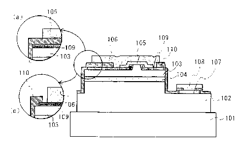
Fig. 1 shows a nitride semiconductor device according to a
first embodiment. The nitride semiconductor device is a
semiconductor laser diode (LD) including an n-type nitride
semiconductor layer 102, an active layer 104, and a p-type
nitride semiconductor layer 103 deposited in that order on a
substrate 101. The p-type nitride semiconductor layer 103 has
a ridge stripe. The ridge stripe may is formed by partially
etching the p-type nitride semiconductor layer or other
processes to function as an effective refractive-index
waveguide. Alternatively, the ridge stripe may be formed by
partially etching a region from the p-type semiconductor layer
to the n-type nitride semiconductor layer to function as a
real refractive-index waveguide, or by selective growth. The
ridge stripe is not necessarily formed in a mesa manner, in
which the width of the stripe is gradually reduced upward.
For example, it may be in a reversed mesa manner, in which the
width is reduced downward, a parallelepiped manner whose side
surfaces perpendicular to the surfaces of layers, or in
CA 02458134 2004-02-19
- 35 -
combination of these manners. The waveguide in the strip does
not necessarily have a constant width. After the completion
of the ridge stripe, the semiconductor layer may be further
deposited at both sides and on the surface of the ridge strip
to make an embed laser device. Alternatively, the waveguide
may have a gain waveguide structure without a ridge. The
nitride semiconductor device may include a current
constriction layer formed of a high-resistance film
(insulative film). The current constriction layer may be
provided in the n-type semiconductor layer or the p-type
semiconductor layer, but preferably in the p-type
semiconductor layer. More specifically, the current
constriction layer, in the n-type or p-type semiconductor
layer, may be provided in each boundary of the contact layer,
cladding layer, guide layer, cap layer, active layer, and so
forth, or in each layer of the contact layer, cladding layer,
guide layer, and so forth. Since the formation of the current
constriction layer requires that deposition be suspended, the
current constriction layer, preferably, formed of a
composition capable of preventing the formation of an
insulative oxide layer, which exhibits an interface state
density to reduce the current injection efficiency.
Alternatively, on resuming the deposition, a very small
thickness of the redeposited film surface may be removed by
etching back the film so that the surface causing the
resistance to increase is eliminated. Exemplary materials of
the current constriction layer include AIN and AlGaN with a
high Al crystal ratio. Preferably, AIN is used because it is
CA 02458134 2004-02-19
- 36 -
highly insulative and allows continuous deposition in
succession to the preceding deposition in the same apparatus.
In addition, since AIN is easily removed with an acid or the
like, a current conduction region, which is formed by removing
the AIN, can be readily provided without damaging other
portions of the device. Furthermore, AIN is suitable for
light confinement because of its low refractive index. The
current constriction layer has a thickness sufficient to block
current. For the formation of a current conduction region as
the waveguide region, selective growth may be applied to the
region other than the current conduction region, or an opening
may be provided in the continuously deposited layer.
A first insulating layer 109 extends from the side surfaces of
the ridge stripe to the upper surfaces of the p-type nitride
semiconductor layer 103 continuing from the ridge stripe. A
first p electrode 105 extends over the upper surfaces of the
ridge and the first insulating layer 109, and a first n
electrode 107 extends on the upper surface of the n-type
nitride semiconductor layer 102. A second insulating layer
110 having an opening at the upper surface of the first n
electrode 107 extends from the upper surface of the first n
electrode 107 to the upper surface of the first insulating
layer 109. A second p electrode 106 in contact with the
second insulating layer 110 and first p electrode 105 is
provided over the p-type nitride semiconductor layer 103. A
second n electrode 108 is also provided on the first n
electrode 107.
In order to orient the ridge stripe in the direction of
CA 02458134 2004-02-19
- 37 -
the resonator, a pair of resonance planes may be provided on
the end surfaces of the device by cleavage or etching. For
cleavage, the substrate and the semiconductor layer must have
cleavage characteristics facilitating the formation of
specular surfaces. Otherwise, the resonance planes can be
formed by etching. In this instance, the etching may be
performed simultaneously with the step of exposing the surface
of the n electrode to reduce the total number of production
steps. Alternatively, the resonance planes may be formed
together with the formation of the ridge stripe. Although the
resonance planes may be formed simultaneously with any other
step to reduce the total number of steps, as above, they are
preferably provided in a separate step from the viewpoint of
preparing superior resonance planes. The resulting resonance
planes by cleavage or etching may have a single-layer or
multilayer reflective layer to efficiently reflect light
emitted from the active layer 104. One of the resonance
planes has a relatively high reflectance so as to reflect
light inside the waveguide region, and the other face has a
relatively low reflectance so as to allow light to go outside.
In the first embodiment, the second insulating layer 110
and the first p electrode 105 are separated. A first p
electrode may be provided in such a manner as to cover the
surface of the p-type nitride semiconductor layer. However,
the first p electrode having such a large area becomes liable
to peel off unless the adhesion of the first p electrode to
the first insulating layer is good. In the first embodiment,
the first p electrode 105 lies at least in the vicinity of
CA 02458134 2004-02-19
- 38 -
both side surfaces of the ridge stripe, apart from the ends of
the p-type nitride semiconductor layer 103. Thus, the contact
area of the first p electrode 105 with the first insulating
layer 109 is reduced to prevent the electrode from peeling
even if the adhesion to the first insulating layer 109 is low,
in comparison with the case where the first electrode is
formed from one end to the other across the surface of the
semiconductor layer. In addition, the first p electrode 105
is separate from the second insulating layer 110. Accordingly,
the second p electrode 106 is in contact with the first
insulating layer 109. The second insulating layer 110 has
relatively thick portions to prevent short circuiting between
the p-side electrodes and the n-side electrodes. Consequently,
rather deep recesses are formed between both sides of the
ridge stripe and the second insulating layer 110 to increase
the irregularity at the joint surface of the second p
electrode 106. This irregularity increases the joint area to
help prevent the second electrode from peeling.
On the other hand, since the first insulating layer 109,
which is provided to limit current injection to the region at
the upper surface of the ridge stripe, lies close to the
waveguide region of the ridge stripe, the thickness of the
first insulating layer 109 affects the efficiency of light
confinement. Therefore, the thickness may not be readily
increased. However, some insulting layer materials require a
small thickness. A thin first insulating layer may have
rather low-insulation portions. Even in such a case, current
injection is limited to the vicinity of the ridge stripe by
CA 02458134 2004-02-19
- 39 -
expanding the second insulating layer 110 to the regions
relatively close to the ridge stripe between the second p
electrode 106 and the first insulating layer 109.
The first insulating layer 109 may have the same width as
the p-type nitride semiconductor layer 103, as shown in (a) of
Fig. 1. The first insulating layer 109, which is formed
before the formation of the first p electrode 105, undergoes
heat treatment when the first p electrode 105 is subjected to
heat treatment. The heat treatment increases the strength or
atomic bonding force of the insulating layer in comparison
with a simply deposited insulating layer, thus increasing the
adhesion at the interface with the p-type nitride
semiconductor layer 103. By extending the first insulating
layer 109 to the ends of the upper surface of the p-type
nitride semiconductor layer 103, where the second insulating
layer 110 is disposed, the adhesion of the second insulating
layer 110 can be increased.
The second p electrode 106 may formed not to be in contact
with the second insulating layer 110, as shown in (b) of Fig.
1. In particular, if the device is mounted face down, heat is
conducted to the second p electrode 106 to increase the volume
of the electrode due to thermal expansion. Thus, the second p
electrode 106 becomes liable to extend toward the side
surfaces of the p-type nitride semiconductor layer 103. In
addition to heat, pressure is placed on the second p electrode
106 and consequently the second electrode becomes liable to be
extended towards the side surfaces. Accordingly, the second p
electrode 106 is separated from the second insulating layer
CA 02458134 2004-02-19
- 40 -
110 to prevent short circuiting resulting from the extension
of the second p electrode 106.
Preferably, the first insulating layer, not only in the
first embodiment but also in the subsequent embodiments, is
formed of at least one compound selected from the group
consisting of SIN, BN, SiC, AlN, AlGaN, and oxides containing
at least one element selected from among Si, Ti, V, Zr, Nb, Hf,
and Ta. More preferably, BN, AlN, AlGaN, and oxides of Zr, Hf,
and Si are used.
Preferably, the thickness of the first insulating layer is
set in the range of 10 to 10,000 A, and more preferably in the
range of 100 to 5,000 A. This is because a thickness of less
than 10 A impairs secure insulation and a thickness of more
than 10,000 A negatively affects the uniformity of the
insulating layer to result in a degraded insulation. In
addition, the above-described preferred range leads to a
uniform layer having a good difference in refractive index
from that of the ridge strip at the sides of the ridge strip.
The second insulating layer 110 may be provided over the
entire surface of the composite except the upper surface of
the ridge strip, preferably including the side surfaces of the
p-type nitride semiconductor layer 103 and active layer 104,
which have been exposed by etching. Preferably, the second
insulating layer 110 is formed of at least one compound
selected from the group consisting of SIN, BN, SIC, AIN, AlGaN,
and oxides containing at least one element selected from among
Si, Ti, V, Zr, Nb, Hf, and Ta. More preferably, the second
insulating layer 110 comprises a single layer or multilayer
CA 02458134 2004-02-19
- 41 -
film of Si02, A1203, Zr02, or Ti02=
Second Embodiment
Fig. 2 shows a nitride semiconductor device according to a
second embodiment of the present invention. The nitride
semiconductor device is a semiconductor laser diode (LD)
including an n-type nitride semiconductor layer 202, an active
layer 204, and a p-type nitride semiconductor layer 203
deposited on a substrate 201, as in the first embodiment. The
p-type nitride semiconductor layer 103 has a ridge stripe. A
first p electrode 205 is formed so as to cover a wide region
of a first insulating layer 209. A second insulating layer
210 is formed so as to overlap the first p electrode 205 in
regions apart from the ridge stripe. A second p electrode 206
is formed on the first p electrode 205 and the second
insulating layer 210. Hence in the second embodiment, the
second p electrode 206 is not in contact with the first
insulating layer 209. The light confinement in the waveguide
region may be varied depending on the depth (height) of the
ridge stripe of the first insulating layer 209, and the light
confinement may be controlled by increasing the thickness of
the first insulating layer 209. In this instance, the first p
electrode 205 having a large area helps to reduce heat
concentration and increases the joint region of the first and
second electrodes 205 and 206 to enhance the adhesion.
The second p electrode 206 may be disposed in such a
manner as not to be in contact with the second insulating
layer 210, as shown in (a) of Fig. 2. Thus, the second p
CA 02458134 2004-02-19
- 42 -
electrode 206 is less adhesive to insulating layers and is
only in contact with the first p electrode 205.
Consequently,
the second p electrode 206 becomes hard to peel. Furthermore,
although heat application in face-down mounting may cause
deformation of the second p electrode 206, as described in the
first embodiment, this structure prevents the deformed second
p electrode from spreading to the n-type nitride semiconductor
layer 202 to achieve an device exhibiting high reliability.
Third Embodiment
Fig. 3 shows a nitride semiconductor device according to a
third embodiment of the present invention. This nitride
semiconductor device is a semiconductor laser diode (LD)
including an n-type nitride semiconductor layer 302, an active
layer 304, and a p-type nitride semiconductor layer 303
deposited on a substrate 301, as in the first embodiment. The
p-type nitride semiconductor layer 303 has a ridge stripe. In
the third embodiment, an adhesion layer 311 is provided
between a second p electrode 306 and at least one of a first
insulating layer 309 and a second insulating layer 310. The
adhesion layer 311 complements the adhesion between the second
p electrode 306 and the first insulating layer 309 or the
second insulating layer 310, and is not placed on the upper
surface of the ridge stripe, where a first p electrode 305 is
joined to the second p electrode 306, or the vicinity of the
upper surface.
The electrodes and insulating layers need to be adhesive
to not only the underlying layers, but also the overlying
CA 02458134 2004-02-19
- 43 -
layers. These requirements are satisfied by using different
materials for the upper layer and lower layer in each
electrode. The adhesion layer 311 further enhances the
' adhesion. Fig. 3 shows that part of the adhesion layer 311
lies between the first p electrode 305 and the second p
electrode 306. Alternatively, the adhesion layer 311 may be
formed not to be in contact with the first p electrode 305.
The material of the adhesion layer 311 does not
necessarily have a low contact resistance with the p-type
nitride semiconductor layer 303 as much as that of the first p
electrode 305, or superior adhesion to the semiconductor layer
303. The material, also does not require reducing the
interface resistance between the first p electrode 305 and the
second p electrode 306. In addition, the material does not
need to have both high adhesion to the electrodes and high
insulation as much as those of the first and second insulating
layers 309 and 310. Specifically, the adhesion layer 311 may
be conductive or insulative, and requires only adhesion to the
insulating layers and electrodes. Accordingly, the adhesion
layer 311 may be formed of a high-resistance material
unsuitable for use as an electrode, as long as the material is
adhesive to the insulating layers 309 and 310. Furthermore,
the adhesion layer 311 is formed in a multilayer form in which
the uppermost sublayer is formed of a material adhesive to the
second p electrode 206, thus enhancing the adhesion.
The adhesion layer 311 may comprise a single-layer or
multilayer film. For a multilayer film, the lowermost
sublayer of the adhesion layer 311 is formed of a material
CA 02458134 2004-02-19
- 44 -
adhesive to the insulating layers, and the uppermost sublayer
is formed of a material adhesive to the second p electrode 306.
Thus superior adhesion can be provided.
As a preferable material for the adhesion layer, a
conductive material or an insulating material can be used. If
the upper layer of the first p electrode 305 is formed of Pt;
the lower layer of the second n electrode 306, Rh; and their
joint region, an element of the platinum group, the uppermost
sublayer of the adhesion layer 311 may be formed of an element
other than the elements of the platinum group, such as Au.
Also, if both the upper layer of the first p electrode 305 and
the lower layer of the second p electrode 306 are formed of
the same material, such as Pt, the uppermost sublayer of the
adhesion layer 311 may be formed of a different material, such
as Au. It is particularly preferable that the uppermost
sublayer of the adhesion layer 311 be formed of an elemental
metal of the platinum group or an alloy constituted of
homologous elements in the platinum group. If, for example,
the upper layer of the first p electrode 305 is formed of Pt;
the lower layer of the second p electrode 306, Rh; and their
joint region, an element of the platinum group, the uppermost
sublayer of the adhesion layer 311 is preferably formed of Pt
so that all the layers in the joint region are composed of
elements of the platinum group. If both the upper layer of
the first p electrode 305 and the lower layer of the second p
electrode 306 are formed of the same Pt, the uppermost
sublayer of the adhesion layer 311 is preferably formed of Pt
so that all the layers in the joint region are composed of the
CA 02458134 2004-02-19
- 45 -
same element. Since the second p electrode 306 is provided on
layers with irregular surfaces formed of the same material,
the above-described structures help establish extremely
superior adhesion. Pt is particularly preferable, among
elements of the platinum group. The lowermost sublayer of the
adhesion layer 311 is preferably formed of Ti.
The adhesion layer 311 is preferably larger than the
second p electrode 306. However, the adhesion layer 311 and
the second p electrode 306 may have substantially the same
size, as shown in (a) of Fig. 3. Alternatively, the adhesion
layer 311 may be positioned under the second insulating layer
310, as shown in (b) of Fig. 3. Thus, short circuiting in
face-down mounting can be prevented.
Fourth Embodiment
Fig. 4 shows a nitride semiconductor device according to a
fourth embodiment of the present invention. This nitride
semiconductor device is a semiconductor laser diode (LD)
including an n-type nitride semiconductor layer 402, an active
layer 404, and a p-type nitride semiconductor layer 403
deposited on a substrate 401, as in the first embodiment. The
p-type nitride semiconductor layer 403 has a ridge stripe. In
the fourth embodiment, an adhesion layer 411 is provided
between a first p electrode 405 and a first insulating layer
409. This structure is provided by forming the adhesion layer
411 before forming the first p electrode 405. In this
structure, since the adhesion layer 411 is located closer to
the p-type nitride semiconductor layer 403, light confinement
CA 02458134 2004-02-19
- 46 -
in the waveguide region can be controlled by varying the
position of the adhesion layer 411. If a material, which is
selected for the lower layer of the first p electrode 405 in
prime consideration of the ohmic contact with the p-type
semiconductor layer 403, has significantly high light
absorption coefficient, optical characteristics may be
degraded. In this instance, by providing the adhesion layer
411 under the first electrode 405, this negative effect can be
alleviated. In addition, peeling of the first electrode 405
from the first insulating layer 409 can be reduced even if the
adhesion between the first p electrode 405 and the first
insulating layer 409. Since the adhesion layer 411 is formed
before the first p electrode 405, the adhesion layer 411 is
also subjected to heat treatment. Consequently, the adhesion
between the first insulating layer 409 and the adhesion layer
411 can be enhanced.
Furthermore, by forming the adhesion layer 411 in such a
manner as to reach the upper surfaces of the second insulating
layer 410, the peel of the second electrode 406 causing
degradation of device properties can be prevented. The
adhesion layer 411 may extend on the surface of the first
insulating layer 409 in such a manner as not to overlap the
second insulating layer 410 and the second electrode 406 or as
to be separated, as shown in (a) of Fig. 4. Thus, short
circuiting in face-down mounting can be prevented.
Alternatively, the adhesion layer 411 may extend to the top of
the first insulating layer 409 on the side surfaces of the
ridge stripe, as shown in (b) of Fig. 4. Since the adhesion
CA 02458134 2004-02-19
- 47 -
layer is disposed close to the waveguide region, ripple can be
reduced due to, for example, absorption of stray light. Thus,
a superior far field pattern (FFP) can be provided.
Fifth Embodiment
Fig. 5 shows a nitride semiconductor device according to a
fifth embodiment of the present invention. This nitride
semiconductor device is a semiconductor laser diode (LD)
including an n-type nitride semiconductor layer 502, an active
layer 504, and a p-type nitride semiconductor layer 503
deposited on a substrate 501, as in the first embodiment. The
p-type nitride semiconductor layer 503 has a ridge stripe. In
the fifth embodiment, a first p electrode 505 is disposed only
on the upper surface of the ridge stripe. In order to form
the first p electrode 505 with the same width as the ridge
stripe of a narrow LD, the first electrode 505 is deposited at
a desired width on a flat semiconductor layer, and the
semiconductor layer is etched to form a ridge stripe through
the first electrode 505 as a mask. In such a self-aligning
process applied to etching of semiconductors, dry etching is
preferably performed using a chlorine-based gas. In this
instance, the first p electrode 505 functioning as an etching
mask has an upper layer formed of an element of the platinum
group. The surface of the first p electrode 505 is relatively
smooth even after etching. If the first electrode 505 is
formed after the formation of the ridge stripe, a
semiconductor layer is etched through a Si02 or resist mask
with a desired ridge width. After removing the mask, the
CA 02458134 2004-02-19
- 48 -
first electrode 505 is deposited in the region where the mask
has been removed, on the semiconductor layer. Therefore, part
of the mask may be left on the surface of the semiconductor
layer. This remaining mask may reduce the ohmic contact
properties and adhesion between the first p electrode 505 and
the semiconductor layer. In contrast, the structure of the
fifth embodiment reduces the possibility of such problems.
As mentioned in Fig. 5, the first p electrode 505 with
substantially the same width as the ridge stripe limits the
contact area between the first p electrode 505 and the second
p electrode 506 to the width of the ridge stripe. Accordingly,
by providing a joint region of a platinum group element using
the upper layer of the first p electrode 505 and the lower
layer of the second p electrode 506, an extremely good
adhesion can be established even in a small contact area. In
addition, the increase in interface resistance can be
prevented and thus, the resulting device exhibits a low
operating voltage and stable and reliable operating
characteristics. If a metal layer 512, described later, is
disposed between the first and second p electrodes 505 and 506,
the join region is provided between the first electrode 505
and the metal layer 512 and between the metal layer 512 and
the second electrode 506) to provide the same effects.
When the ridge stripe is formed in a self-aligning process,
the upper surface of the first p electrode 505 is exposed to a
chlorine-based gas for etching a semiconductor layer or a
fluorine-based gas for etching a Si02 layer to produce a
chloride or a fluoride, but not oxide. However, the layer of
CA 02458134 2004-02-19
- 49 -
an element of the platinum group limits the reaction with the
chlorine-based gas or the fluorine-based gas to the vicinity
of its surface. The composition inside the upper layer of the
first p electrode 505 is therefore maintained as it was when
deposited. If the chlorine or fluorine product is stable and
insulative, the surface of the upper layer is cleaned so as to
expose a region inside the upper layer not containing the
product because an interface resistance occurs at the
interface between the product and the second p electrode 506.
Then, the second electrode is formed on the exposed region to
prevent the ohmic characteristics from deteriorating.
When the n-type nitride semiconductor 502 is exposed, a
metal layer 512 shown in Fig. 5 may be used as a mask. The
metal layer 512 is formed for example, of an element of the
platinum group to a predetermined shape on the first p
electrode 505, and etching is performed until the n-type
nitride semiconductor layer 502 is exposed. The metal layer
512 used as a mask may be removed later or left as is. If the
metal layer 512 is left to be used as part of the electrodes,
it is preferable that the first insulating layer 509 be
disposed at both sides of the ridge stripe in advance and that,
the first insulating layer 509 and the upper surface of the
ridge stripe are then covered with the metal layer 512 to form
the structure as shown in Fig. 5. In this instance, the metal
layer 512, which is in contact with the first electrode 505,
is formed of an element of the platinum group to function as
the lower layer of the second electrode 506. Preferably, the
metal layer 512 is formed of platinum.
CA 02458134 2004-02-19
- 50 -
The etching mask for exposing the n-type nitride semiconductor
502 may be a Si02 film or the like. In this case, the Si02
film is removed after the n-type nitride semiconductor layer
502 has been exposed, and the first insulating layer 509 is
formed at both sides of the ridge stripe. Then, the second p
electrode 506 is provided in such a manner as to be in contact
with the first electrode 505.
The second p electrode 506 may not be in contact with the
second insulating layer 510, as shown in (a) of Fig. 5, to
prevent short circuiting in face-down mounting. In addition,
since the second p electrode 506 is in contact with only the
metal layer 512, the adhesion between the electrodes can be
enhanced.
Sixth Embodiment
Figs. 8A and 8B show a nitride semiconductor device
according to a sixth embodiment of the present invention. Fig.
8B is a sectional view taken along line X-Y in Fig. 8A. The
nitride semiconductor device is a light-emitting diode (LED)
including an n-type nitride semiconductor layer 802, an active
layer 804, and a p-type nitride semiconductor layer 803
disposed in that order on a substrate 801. The p-type nitride
semiconductor layer 803 is provided with a first p electrode
805 and a second p electrode 806 on its upper surface, and the
n-type nitride semiconductor layer 802, which is exposed by
etching from the p-type nitride semiconductor layer side, is
provided with a first n electrode 807 and a second n electrode
808 on its surface. The LED does not have a ridge stripe as
CA 02458134 2004-02-19
- 51 -
in LDs, and light emitted from the active layer 804 is
radiated to outside through the p-type nitride semiconductor
layer 803, n-type nitride semiconductor layer 802, or side
surfaces of the composite. The first p electrode 805 is
disposed over substantially the entire upper surface of the p-
type nitride semiconductor layer 803 and is joined with the
second p electrode 806 in a joint region 813. The first
electrode 805 has a thickness capable of transmitting light
from the active layer 804, and is subjected to heat treatment
so that a transparent electrode comes into ohmic contact with
the p-type nitride semiconductor layer 803.
In the LED according to the sixth embodiment, the joint
region between the transparent first p electrode 805 and the
second p electrode 806 is small and, accordingly, a high
current flows in the joint region 813 when the electrodes are
energized. Therefore, by providing the joint region 813 with
a good adhesion and a low resistance, the resulting LED
exhibits superior reliability.
The LED is not limited to the form shown in Figs. 8A and
8B. For example, the first p electrode 805 may have a large
thickness to reduce the sheet resistance and an opening for
extracting light. In another form of the LED, the p-type
nitride semiconductor layer 803 has an uneven surface whose
recesses are filled with an insulating film. Thus, various
modifications may be made.
EXAMPLES
Examples of the nitride semiconductor device of the
CA 02458134 2004-02-19
- 52 -
present invention will now be described using semiconductor
laser devices. The form of the present invention is, however,
not particularly limited to these laser devices and the
invention may be applied to other nitride semiconductor
devices including an n-type nitride semiconductor layer, an
active layer, and a p-type nitride semiconductor layer. In
addition to these laser devices having the following
structures, the present invention may be applied to other
lasers and LEDs. Exemplary nitride semiconductors include
Group III-V nitride semiconductors such, as GaN, AlN, and InN,
including their mixed crystals AlGaN, InGaN, and AlInGa.
These nitride semiconductors may further contain B, P, or the
like. Nitride semiconductors are deposited by metal organic
phase epitaxy (MOVPE), metallorganic chemical vapor deposition
(MOCVD), hydride vapor phase epitaxy (HVPE), molecular beam
epitaxy (MBE), or any other deposition process.
EXAMPLE 1
Substrate
A c-plane sapphire is used as the substrate. However, the
substrate is not particularly limited to this, and may
comprise an R-plane or A-plane sapphire, SiC, Si, spinel, GaN,
or any other material. For a GaN substrate, a nitride
semiconductor layer (AlGaInN) is deposited by epitaxial
lateral overgrowth (ELOG) in which a growing substrate, such
as sapphire and GaAs, provided with a protective layer for
preventing the growth is subjected to selective lateral growth.
The growing substrate is subsequently removed and, thus, a GaN
CA 02458134 2004-02-19
- 53 -
substrate (nitride semiconductor substrate) having good
crystallinity is obtained. Doping of Si, oxygen, or the like
during the deposition of the nitride semiconductor layer can
allow the conductivity to be adjusted. The resulting GaN
substrate by ELOG unevenly includes high-dislocation-density
regions and low-dislocation-density regions, depending on
deposition conditions and the form of the protective layer.
Therefore, in a laser device requiring reliability at a high
current density, the waveguide is provided in a low-
dislocation-density region to produce superior characteristics.
If an insulative substrate, such as sapphire, is used, the p
electrode and the n electrode are provided on the same side of
the substrate. If a conductive substrate, such as GaN, is
used, the p electrode and the n electrode may be provided on
the same side, or the n electrode may be provided on the
backside of the substrate, not having the functional layers.
Base Layer
An undoped GaN layer is deposited to a thickness of 2.5 gm
at a temperature of 1,050 C, and a Si02 protective layer is
formed to a thickness of 0.27 gm. Striped openings (unmasked
regions) are formed in the Si02 protective layer by etching.
The stripes of the opening have a width of 1.8 gm and extend
perpendicular to the original flat of the substrate. The
width ratio of the protective layer to the openings is set at
6:14. Then, undoped GaN is further deposited to a thickness
of 15 gm in the openings. The GaN in the openings grows to
extend on the Si02 layer in the lateral direction and
_
CA 02458134 2004-02-19
- 54 -
ultimately covers the Si02 layer. The base layer may be formed
of AlGaN, InGaN, AlInGAN, or the like, instead of GaN.
Buffer Layer
A Si-doped A10.02Ga0.98N buffer layer is deposited to a
thickness of 1 gm at a temperature of 500 C using
trimethylgallium (TMG) and ammonia (NH3).
N-Type Contact Layer
A n-type contact layer of Si-doped n-A10.02Ga0.98N is
subsequently deposited to a thickness of 3.5 gm at a
temperature of 1,050 C using trimethylgallium (TMG) and
ammonia (NH3) as material gases and silane gas as a dopant.
The thickness of the resulting n-type contact layer is set in
the range of 2 to 30 gm.
Crack-Free Layer
Then, Si-doped n-In0.05Ga0.95N crack-free layer is deposited
to a thickness of 0.15 gm at a temperature of 800 C using TMG,
NH3, and trimethylindium (TMI). The crack-free layer may be
omitted depending on the type of substrate or the composition
of other layers.
N-Type Cladding Layer
An A layer comprising undoped A10.05Ga0.095lq and subsequently
a B layer comprising Si-doped GaN are deposited to a thickness
of 50 A each at a temperature of 1,050 C using
trimethylaluminum (TMA), TMG, and NH3 as material gases. This
CA 02458134 2004-02-19
- 55 -
sequence of depositions is repeated 110 times to alternately
deposit the A layers and the B layers to a total thickness of
1.1 m. Thus, an n-type cladding layer having a layered
structure (superstructure) is formed. In order to achieve a
difference in refractive index sufficient to function as a
cladding layer, the Al crystal ratio in the AlGaN mixed
crystal layer may be set in the range of 0.02 to 0.3. Each
layer of the cladding layer, having the superstructure may
have other crystal ratios or may be formed of InGaN or the
like, and any other composition may be selected to be
effective in confining light in the active layer. It is not
necessary that the n-type cladding layer has the
superstructure, and may be composed of, for example, a single
layer of Al0.05Ga0.95N.
N-Type Light Guide Layer
An n-type light guide layer of undoped GaN is subsequently
deposited to a thickness of 0.15 gm at a similar temperature to
the deposition of the cladding layer using TMG and NH3. This
layer may be doped with an n-type dopant. The light guide
layer may be formed of InGaN, AlGaN, AlInGaN, and the like
depending on the composition of the active layer, or may be
omitted depending on the composition of the cladding layer.
Active Layer
A Si-doped 1n0.02Ga0.98N barrier layer is deposited to a
thickness of 140 A at a temperature of 800 C using TMI, TMG,
and NH3 as material gases and silane gas as a dopant. After
CA 02458134 2004-02-19
- 56 -
removing the silane gas, an undoped In0.1Ga0.9N well layer is
deposited to a thickness of 70 A. This sequence of
depositions is repeated twice, and finally, a Si-doped
In0.02Ga0.98N barrier layer is deposited to a thickness of 140 A.
Thus, an active layer with a total thickness of 560 A having a
multi-quantum well (MQW) structure is provided. The number of
the MQW depositions is preferably in the range of about 2 to
30. The MQW structure may be formed of other compositions,
such as InGaN/GaN, AlGaN/InGaN, InGaN/AlInGaN, and AlGaN/
AlInGaN. A single-quantum well (SQW) structure may be applied.
P-Type Electron Confinement Layer
A Mg-doped A10.25Ga0.751q P-type electron confinement layer
is subsequently deposited to a thickness of 30 A at a similar
temperature in a N2 atmosphere. The p-type electron
confinement layer is further deposited to a thickness of 70 A
in a H2 atmosphere. The p-type electron confinement layer may
be of single-layer film deposited at a temperature similar to
the deposition temperature of the active layer. The p-type
electron confinement layer may be formed of other compositions
such as AlGaN, AlInGaN, and GaN. If the thickness is large,
InGaN may be used.
P-Type Light Guide Layer
A p-type light guide layer of undoped GaN is deposited to
a thickness of 0.15 gm at a temperature of 1,050 C using TMG
and NH3 as material gases. Although the p-type light guide
layer is not doped in Example 1, it may be doped with Mg. The
p-type light guide layer may be formed of InGaN, AlGaN,
CA 02458134 2004-02-19
- 57 -
AlInGaN, or the like depending on the composition of the
active layer.
P-Type Cladding Layer
An A layer of undoped A10.08Ga0.92N is deposited to a
thickness of 80 A and a B layer of Mg-doped GaN is deposited
to a thickness of 80 A on the A layer. This sequence of
depositions is repeated 28 times to alternately deposit the A
layers and the B layers to a total thickness of 0.45 gm. Thus,
a p-type cladding layer having a layered structure
(superstructure) is provided. If at least one of the A and B
layers comprises nitride semiconductor containing Al and the
bandgap energies of the two layers are different from each
other, the crystallinity of the cladding layer can be enhanced
by so-called modulation dope in which one of the two layers is
doped with a larger amount of dopant than the other layer is.
However, both the A and B layers may be equally doped. Each
layer of the cladding layer, having the superstructure may
have other crystal ratios or may be formed of InGaN or the
like, and any other composition may be selected to be
effective in confining light in the active layer. The p-type
cladding layer may need not to bethe superstructure and may be
composed of, for example, a single layer of A10.05Ga0.95N.
P-Type Contact Layer
Finally, a p-type contact layer of Mg-doped GaN is
deposited to a thickness of 150 A on the p-type cladding layer
at a temperature of 1,050 C. The p-type contact layer may be
CA 02458134 2004-02-19
- 58 -
formed of a p-type semiconductor expressed by the formula
InxAlyGai_x_yN (x 0, y 0, x + y 1), and particularly Mg-
doped GaN establishes the best ohmic contact with the p
electrode. After the deposition, the resulting composite is
annealed to reduce the resistance of the p-type layers at
700 C in a nitride atmosphere in a reaction chamber.
Exposure of N-Type Contact Layer
The composite of the nitride semiconductor layers taken
out from the reaction chamber is provided with a Si02
protective layer on the surface of the p-type contact layer,
being the uppermost layer of the composite, by reactive ion
etching (RIE) using C12 gas to expose the surface of the n-type
contact layer to which an n electrode is formed. At this
moment, resonance planes may be formed by etching. Although
it is preferable to form the resonance planes simultaneously
with the exposure of the n-type contact layer, it may be
performed in a different step.
Ridge Stripe
In order to provide a waveguide region in a stripe form, a
silicon oxide (primarily Si02) protective layer is deposited to
a thickness of 0.5 gm over substantially the entire surface of
the uppermost layer, i.e., p-type contact layer, by chemical
vapor deposition (CVD) and is, then, etched to a stripe by RIE
using CHF3 gas, through a mask having a predetermined shape
formed over the protective layer by photolithography. The p-
type contact layer is etched with SiC14 gas through the silicon
CA 02458134 2004-02-19
- 59 -
oxide protective layer as the mask, thus forming the ridge
stripe above the active layer. The resulting ridge stripe has
a width of 1.6 gm.
First Insulating Layer
A Zr02 first insulating layer is formed over the surface
of the p-type semiconductor layer through the Si02 mask layer
remaining. The first insulating layer may be provided over
the entire surfaces of the p- and n-type contact layers
through a first n electrode-forming region masked. For
convenience of cutting, regions having no insulating layer may
be provided.
After the formation of the insulating layer, the composite
is subjected to heat treatment at 600 C. If the first
insulating layer is formed of a material other than Si02, heat
treatment at a temperature of 300 C or more, preferably 400 C
or more, and lower than or equal to the decomposition
temperature (1,200 C) of the nitride semiconductor layers
stabilizes the material of the insulating layer. In
particular, if S102 is used as a mask for device processing
after the formation of the first insulating layer, the heat
treatment makes the insulating layer insoluble in a mask
solvent used for removing the Si02 mask. The heat treatment of
the first insulating layer may be omitted, depending on the
material and production step of the first insulating layer, or
may be performed simultaneously with heat treatment of an
ohmic electrode. The order of steps may be appropriately
varied. After the heat treatment, the composite is immersed
CA 02458134 2004-02-19
- 60 -
in a buffered liquid to dissolve and remove the Si02 layer on
the ridge stripe and, thus, the Zr02 over the ridge stripe on
the p-type contact layer (and the first n electrode-forming
region) is removed together with the 5i02 by lift-off. Thus,
the upper surface of the ridge stripe is exposed, but the side
surfaces are covered with the Zr02.
First Electrodes (Ohmic Electrodes)
A first p electrode is formed on the surface of the ridge
stripe and the first insulating layer by sputtering. The
first p electrode comprises a Ni/Au lower layer (100 A/1,500
A) and a Pt upper layer (1,500 A). A first n electrode is
formed on the upper surface of the n-type contact layer. The
first n electrode is formed of Ti/A1 (200 A/8,000 A) to a
stripe form with the same length as the ridge stripe in
parallel with the ridge stripe. These electrodes are
subjected to heat treatment at 600 C in an atmosphere of a
mixture of oxygen and nitrogen gases.
Second Insulating Layer
A resist layer is formed to cover the entire surface of
the first p electrode on the ridge stripe and part of the
upper surface of the first n electrode. Then, Si02 is
deposited over substantially the entire surface of the
composite, and is removed by lift-off to form a second
insulating layer in which the entire upper surface of the
first p electrode and part of the first n electrode are
exposed. The second insulating layer is separate from the
CA 02458134 2004-02-19
- 61 -
first p electrode in such a manner that the first insulating
layer is exposed between them. It is possible that the first
and second insulating layers and the electrodes are not
provided at striped regions having a width of, for example,
about 10 gm between the devices for ease of cutting.
The second insulating layer is disposed over the entire
surface of the composite except the upper surfaces of the
first p and n electrodes. Preferably, the second insulating
layer is formed of at least one compound selected from the
group consisting of SIN, BN, SiC, AIN, AlGaN, and oxides
containing at least one element selected from among Si, Ti, V,
Zr, Nb, Hf, and Ta. More preferably, the second insulating
layer comprises a single-layer or multilayer film of Si02,
A1203, Zr02, or Ti02.
Second Electrodes (Pad Electrodes)
Second electrodes are formed to cover the first electrodes.
Preferably, the second electrodes overlap the second
insulating layer. For the second p electrode, Pt is deposited
to form a lower layer with a thickness of 1,000 A, and Ti, Pt,
and Au are subsequently deposited, in that order, on the lower
layer to thicknesses of 50 A, 1,000 A, and 6,000 A
respectively. For the second n electrode Ni, Ti, and Au are
deposited to thicknesses of 1,000 A, 1,000 A, and 8,000 A,
respectively, in that order. The second p and n electrodes
are respectively brought into contact with the first p
electrode and the first n electrode in a striped manner with
the second insulating layer between the second p and n
CA 02458134 2004-02-19
- 62 -
electrodes.
Cleavage and Formation of Resonator
The resulting composite is grinded to a thickness of about
150 gm, and the rear surface of the substrate is subjected to
scribing. The composite is cleaved from the side having the
nitride semiconductor layers of the substrate to yield a bar-
shaped block of lasers. The cleaved surfaces of the nitride
semiconductor layers are a nitride semiconductor M plane (1-
100) and these surfaces function as resonance planes.
End Surface Protective Layer
Preferably, the resonance planes are each provided with a
protective layer on their surfaces so that light efficiently
resonates in the active layer. It is preferable to provide a
protective layer particularly on the resonance plane on the
light-reflecting side (monitor side) of the device from the
viewpoint of producing a difference in refractive index
between the resonance planes on the light-reflecting side and
the light-emitting side. Exemplary materials of the
protective layer include conductive elements, such as Si, Mg,
Al, Hf, Nb, Zr, Sc, Ta, Ga, Zn, Y, B, and Ti, and their oxides,
nitrides, and fluorides. These materials may be used singly
or in combination and the resulting protective layer may
comprise a single-layer or multilayer film. Preferred
materials contain Si, Mg, Al, Hf, Zr, Y, or Ga.
Semiconductive materials of the protective layer includes AIN,
AlGaN, and EN, and insulative materials includes oxides,
CA 02458134 2004-02-19
- 63 -
nitrides, and fluorides of Si, Mg, Al, Hf, Nb, Zr, Sc, Ta, Ga,
Zn, Y, and B.
In Example 1 the end surface protective layer of the
resonance plane on the light-reflecting side comprises a
dielectric multilayer film including Si02 layers and Zr02
layers. Specifically, the protective layer includes a Zr02
protective sublayer formed by sputtering and a high-reflective
sublayer formed by depositing six pairs of S102 and Zr02 layers
on the Zr02 protective sublayer. The thicknesses of the
protective sublayer and the high-reflective sublayer are each
appropriately set accordingly to the wavelength of light from
the active layer. The resonance plane on the light-emitting
side may be or does not need to be provided with a protective
layer including a first low-reflective sublayer of Zr02, Nb205,
or A1203 and a second low-reflective sublayer of Si02.
Finally, the bar-shaped block of devices is subjected to
scribing substantially parallel to the ridge stripe and is cut
into chips of the nitride semiconductor laser device of the
present invention. The resulting nitride semiconductor laser
device can produce continuous oscillation with an emission
wavelength of 405 nm, a threshold current density of 2.0 kA/cm2,
and a high power of 60 mW at room temperature without peeling
of the electrodes.
EXAMPLE 2
In Example 2, the second insulating layer overlaps the
first p electrode. The laser device of Example 2 is prepared
as in Example 1, except that the second insulating layer is
_ _
CA 02458134 2004-02-19
- 64 -
formed as follows.
Second insulating layer
After the formation of the first electrodes, a Si02 second
insulating layer is formed over substantially the entire
surface of the composite. Then, the entire surface over the
ridge stripe of the first p electrode, part of the surfaces of
the first p electrode at both sides of the ridge stripe, and
part of the surface of the first n electrode are exposed by
dry etching with a resist. Thus, the side surfaces of the
composite and part of the first p and n electrodes are covered
with the second insulating layer. Although the first
insulating layer is not exposed in Example 2, it may also be
exposed.
Second electrodes (pad electrodes)
Second electrodes are formed to overlap the second
insulating layer by sputtering. For the second p electrode,
Pt is deposited to form a lower layer with a thickness of
1,000 A, and Ti, Pt, and Au are subsequently deposited, in
that order, on the lower layer to thicknesses of 50 A, 1,000 A,
and 6,000 A, respectively. For the second n electrode, Ni, Ti,
and Au are deposited to thicknesses of 1,000 A, 1,000 A, and
6000 A, respectively, in that order. The second p and n
electrodes are respectively brought into contact with the
first p electrode and the first n electrode in a striped
manner with the second insulating layer between the second p
and n electrodes. The resulting nitride semiconductor laser
_ _
CA 02458134 2004-02-19
- 65 -
device can produce continuous oscillation with an emission
wavelength of 405 nm, a threshold current density of 2.0 kA/cm2,
and a high power of 60 mW at room temperature, without peeling
of the electrodes.
EXAMPLE 3
In Example 3, an adhesion layer is formed. After forming
each layer up to the first insulating layer as in Example 1, a
first p electrode is formed by depositing Ni, Au, and Pt to
thicknesses of 100 A, 1,500 A, and 1,500 A, respectively, in
that order on the first insulating layer. Then, a second
insulating layer is formed of two pairs of Si02 and TiO2 layers
(1,500 A/1,000 A). In this instance, the second insulating
layer is disposed at a distance of about 225 gm from the first
p electrode. A Ti/Pt adhesion layer (100 A/500 A) is formed
from the upper surface of part of the first p electrode to the
upper surface of the second insulating layer through the
exposed portion of the first insulating layer between the
first p electrode and the second insulating layer. Then, a
Pt/Ti/Pt/Au second p electrode (1,000 A/50 A/1,000 A/6,000 A)
is formed from the upper surface of the first p electrode to
the upper surface of the adhesion layer. Other steps are
performed as in Example 1, and thus a nitride semiconductor
laser device is prepared. The resulting nitride semiconductor
laser device can produce continuous oscillation with an
emission wavelength of 405 nm, a threshold current density of
2.0 kA/cm2, and a high power of 60 mW at room temperature,
without peeling of the electrodes.
CA 02458134 2004-02-19
- 66 -
EXAMPLE 4
A nitride semiconductor laser device is prepared as in
Example 1, except for the formation of the first p electrode
and the second p electrode. In Example 4, the first p
electrode comprises a Ni/Au lower layer (100 A/1,500 A) and a
Pt/Ti/Pt upper layer (500 A/100 A/500 A), and the second p
electrode comprises a Pt lower layer (1,000 A) and a Ti/Pt/Au
upper layer (100 A/1,000 A/6,000 A). The resulting nitride
semiconductor laser device can produce continuous oscillation
with an emission wavelength of 405 nm, a threshold current
density of 2.0 kA/cm2, and a high power of 60 mW at room
temperature.
In the present invention, a joint region is provided
between a first electrode, which establishes an ohmic contact
with a semiconductor layer by heat treatment, and a second
electrode for extraction to produce superior adhesion. Thus,
the resulting nitride semiconductor device has extremely
stable and reliable operating characteristics, exhibiting, for
example, low operating voltage and less deterioration with
time even in high-power operation. Furthermore, an adhesion
layer between an electrode and an insulating layer provides a
wide variety of choices in electrode material and insulating
layer material, consequently providing a nitride semiconductor
device exhibiting superior operating voltage and good adhesion.