Note: Descriptions are shown in the official language in which they were submitted.
CA 02458206 2004-02-20
WO 03/019682 PCT/IL02/00676
A THERMOELECTRIC DEVICE FOR COOLING
FIELD OF THE INVENTION
The present invention generally relates to thermoelectric devices for cooling.
More
specifically, the present invention relates to a thermoelectric device having
one cold pole and at least
two heat sinks, wherein said device is useful for cooling.
BACKGROUND OF THE INVENTION
Thermoelectric devices have thermoelectric materials sandwiched between
ceramic plates.
They are solid-state, vibration-free, noise-free heat pumps, pumping the heat
from one surface to
another. If the heat at the hot side is dissipated to the ambient environment,
this assembly becomes
a cooling unit. A thermoelectric module also can be used to generate
electrical power by converting
heat from any source.
Having no moving parts, being small in size and light in weight,
thermoelectric devices have
been widely used in military, medical, industrial, consumer,
scientific/laboratory, electro-optic and
telecommunications areas for cooling.
Thermoelectric cooling or heating, also called "the Pettier Effect," is a
solid-state method of
heat transfer through dissimilar semiconductor materials. Using Bismuth and
copper, in 1834 Jean
Charles Pettier discovered the flip side of Seebeck's thermoelectric effect.
He found that current
driven in a circuit made of dissimilar metals causes the different metals to
be at different
temperatures.
This effect arises in the process of direct current (DC) flowing through a
module that leads to
the transfer of heat from one side of the module to the other. As a result,
one side of the module
cools and the other heats. Temperature differences can be achieved up to
+73°C in a single stage
module and more than +100°C in multistage modules.
Advantages of using thermoelectric modules for cooling or heating:
ecological cleanliness and safety due to the absence of any gas or liquid
agents;
no noise or vibration;
cooling or heating mode is simply changed by reversing the current flow
direction;
miniaturization capabilities, especially with the more recent advent of
micro-electromechanical structures (MEMS); and
functionality in any position relative to the gravitation field, including
weightlessness.
1
CA 02458206 2004-02-20
WO 03/019682 PCT/IL02/00676
Thermoelectric cooling uses the following elements:
a cold pole,
a heat sink and
a DC power source.
The cold pole is cooled because the electrons move from the level of energy of
one of the
semiconductors to the higher level of energy of the second semiconductor. A DC
power source
pumps the electrons from one semiconductor to another. A heat sink discharges
the accumulated
heat energy from the system. A thermoelectric device is defined simply as
semiconductor materials
with dissimilar characteristics, as connected electrically in series and
thermally in parallel, so that two
junctions are created.
The semiconductor materials are negative (N) and positive (P) type, and are so
named
because either they have more electrons (-) than necessary to complete a
special molecular lattice
structure (N-type) or not enough electrons (+) to complete a lattice structure
(P-type). The P and N
semiconductors are joined with a metallic junction to form a rr-type series
circuit, called the "P-N
thermocouple." The extra electrons in the N-type material and the holes left
in the P-type material
are called "carriers" and they are the agents that absorb the heat energy, and
move it from the cold
pole to the heat sink. Heat absorbed at the cold pole is pumped to the heat
sink at a rate
proportional to carrier current passing through the circuit and the number of
couples.
Good thermoelectric semiconductor materials, such as bismuth telluride,
greatly impede
conventional heat conduction from hot to cold areas, yet provide an easy flow
for the carriers. In
addition, these materials have carriers with a capacity for transferring more
heat.
Reference is now made to prior art fig. 1a, which is a combined graph of
relative
temperature 101 vs. distance 102 from the heat load 104, wherein distances 102
are referenced to a
schematic diagram of a thermoelectric device. The upper part of the diagram
above illustrates the
steady-state temperature profile across a typical thermoelectric device from
the load side 104 to the
heat released from the heat sink 140 to the ambient environment 106. A P-type
semiconductor 120
and an N-type semiconductor 110 are connected via insulators 108 to a cold
pole 130 and heat sink
140. A DC power source 115 pumps the electrons from N-type semiconductor 110
to P-type
semiconductor 120. The total steady-state heat that must be rejected by the
heat sink to the
environment may be expressed as follows:
QS = Q~ + V*I + Q~, where:
QS 106 is the heat rejected;
Q~ is the heat absorbed from the load;
V*I is the power input; and
Q~ is the heat leakage.
2
CA 02458206 2004-02-20
WO 03/019682 PCT/IL02/00676
If the heat sink cannot reject enough QS 106 from the system, the system's
temperature will
rise and the cold junction temperature will increase. If the emitted heat
increases, the cooling effect
tends to decrease. Stabilization of the hot pole at 5 to 10 degrees higher
than the ambient
temperature, by using a good heat sink, and by stabilizing the temperature of
the cold pole near the
ambient temperature, contributes to improved coefficient of performance (COP).
Energy may be transferred to or from the thermoelectric system by three basic
modes:
conduction, convection, and radiation. The values of Q~ and Q~ may be easily
estimated; their total,
along with the power input, gives QS, the energy the hot junction heat sink
must dissipate.
Prior art fig. 1 b is a simplified schematic illustration of a standard
Pettier module 100.
Standard module 100 comprises two types of semiconductor elements: N-type
semiconductors 110;
and P-type semiconductors 120. The main feature of standard module 100 is that
the height of the
semiconductor elements is equal to the module height 150. The entire top
surface of standard
module 100 is a heat sink 130, and the entire bottom surface is a cold pole
140. The area of heat
sink 130 is equal to the area of cold pole 140.
Prior art fig. 1c is a schematic diagram of the electricity path 170 through
standard module
100. The current traverses N-type semiconductors 110 and P-type semiconductors
120 serially, with
intermediary traversals of the metal junctions 180. Thus, the primary feature
of electrical path 170
through standard module 100 is the regular alternations: semiconductor - metal
junction -
semiconductor - metal junction.
Thus, it would be desirable to provide an improved and diversified system and
method for
high productivity fiber optic, metallurgical and semiconductor polishing that
overcomes the
problems of prior art.
SUMMARY OF THE INVENTION
Accordingly, it is a principal object of the present invention to provide a
thermoelectric
device with improved heat dissipation characteristics.
It is another object of the present invention to provide a thermoelectric
device with a high
coefficient of performance (COP)
It is yet another object of the present invention to provide a thermoelectric
device with
improved distribution of heat accumulation.
3
CA 02458206 2004-02-20
WO 03/019682 PCT/IL02/00676
It is yet another object of the present invention to provide a thermoelectric
device with
optimum distances between the cold pole and the heat sinks.
It is still another object of the present invention to provide a
thermoelectric device with
high conductivity for electric current and low conductivity for heat.
A thermoelectric device is described including:
a plurality of N-type thermoelectric semiconductor elements;
a plurality of P-type thermoelectric semiconductor elements;
metal junctions between horizontally adjacent semiconductor elements;
special layers between vertically adjacent N-type thermoelectric semiconductor
elements and between vertically adjacent P-type thermoelectric semiconductor
elements;
a cold pole;
at least two heat sinks;
and a source of direct current power interconnected so as to pump electrons
from the
N-type semiconductors to the P-type semiconductors, or to pump holes from the
P-type
semiconductors to the N-type semiconductors,
such that the heat buildup is distributed among more than one heat sink.
The device according has dimensions such that the width of each of the at
least two
heat sinks is substantially greater than the width of the cold pole; the
corresponding area
of each of the at least two heat sinks is substantially greater than the
corresponding area
of the cold pole; and the distance from the cold pole to each of the at least
two heat sinks
is substantially greater than the height of the semiconductor elements.
The track of the electric current is:
(a) N-type semiconductors;
(ii) special layers;
(iii) N-type semiconductors;
(iv) special layers;
(v) metal junction;
(vi) P-type semiconductors;
(vii) special layers;
(viii) metal junction;
(ix) special layers; and
(x) P-type semiconductors.
4
CA 02458206 2004-02-20
WO 03/019682 PCT/IL02/00676
The at least two heat sinks are composed of standard aluminum alloys, and a
thin
film base is interposed between the at least two heat sinks.
Other features and advantages of the invention will become apparent from the
following drawings and description.
BRIEF DESCRIPTION OF THE DRAWINGS
For a better understanding of the invention with regard to the embodiments
thereof,
reference is made to the accompanying drawings, in which like numerals
designate
corresponding elements or sections throughout, and in which:
Prior art fig. 1 a is a combined graph and schematic diagram of thermoelectric
heating.
Prior art fig. 1 b is a simplified schematic illustration of a standard
Pettier module 100.
Prior art fig. 1c is a schematic diagram of the electricity path 170 through
standard
module 100.
Fig. 2a is a simplified schematic illustration of an improved Pettier module
in
accordance with an exemplary embodiment of the present invention;
Fig. 2b is a schematic diagram of the electricity path through an improved
Pettier
module, in accordance with an exemplary embodiment of the present invention;
Fig. 3a is a schematic diagram of a top view for an improved Pettier module,
in
accordance with an exemplary embodiment of the present invention;
Fig. 3b is a schematic diagram of a side view for an improved Pettier module,
in
accordance with an exemplary embodiment of the present invention; and
Fig. 3c is a schematic diagram of a bottom view for an improved Pettier
module, in
accordance with an exemplary embodiment of the present invention.
It will be appreciated that the embodiments described as follows are cited by
way of
example, and that the present invention is not limited to what is particularly
shown and described.
Rather, the scope of the present invention, as defined by appended claims,
includes both
combinations and sub-combinations of the various features described, as well
as variations and
modifications thereof, which would occur to persons skilled in the art upon
reading the
descriptions, and which are not disclosed in the prior art.
CA 02458206 2004-02-20
WO 03/019682 PCT/IL02/00676
DETAILED DESCRIPTION OF EXEMPLARY EMBODIMENTS
Fig. 2a is simplified schematic illustration of an improved Pettier module 200
in
accordance with an exemplary embodiment of the present invention. There are
now two heat
sinks, a heat sink #1 233 and a heat sink #2 236. The width 263 of heat sink
#1 233, and
hence its corresponding area, is considerably greater than the width 260 of
cold pole 140, and
its corresponding area. Similarly, the width 266 of heat sink #2 236, and
hence its
corresponding area, is considerably greater than the width 260 of cold pole
140, and its
corresponding area. The distance from cold pole 140 to heat sink #1 233 and
heat sink #2
236 is considerably greater than the height of semiconductor elements 110 and
120.
Fig. 2b is a schematic diagram of the electricity path through improved
Pettier module
200, in accordance with an exemplary embodiment of the present invention. The
track of the
electric current is N-type semiconductors 110 - special layers 290 - N-type
semiconductors
110 - special layers 290 - metal junction 280 - P-type semiconductors 120 -
special Iayers290
- metal junction 280 - special layers 290 - and P-type semiconductors 120.
Fig. 3a is a schematic diagram of a top view for an improved Pettier module,
in
accordance with an exemplary embodiment of the present invention. Top view 302
shows
heat sink #1 233 and heat sink #2 236, which are composed, for example of
standard
aluminum alloys. Between these heat sinks is a thin film base 320.
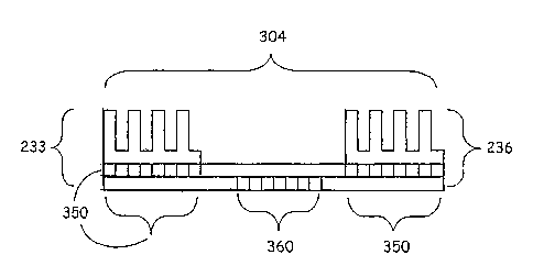
Fig. 3b is a schematic diagram of a side view for an improved Pettier module,
in
accordance with an exemplary embodiment of the present invention. The profile
and height
of heat sinks 233 and 236 are referenced in side view 304, as are the Pettier
elements of
each heat sink. Reference block 360 indicates the electrical interconnections
on the base of
the thin copper film.
Fig. 3c is a schematic diagram of a bottom view for an improved Pettier
module, in
accordance with an exemplary embodiment of the present invention. Bottom view
306 shows
the orientation of cold pole 340.
6