Note: Descriptions are shown in the official language in which they were submitted.
CA 02458535 2004-02-24
ELECTROPHOTOGRAPHIC PRINTING DEVICE
The invention relates to an electrophotographic printing device with a toner
developer unit, an exposure device, a developer drum, a photo-conductor, a
transfer unit and
a grounded charging device, wherein the substrate to be imprinted is moved,
lying on a
transport device, past the transfer zone of the transfer unit and the toner
image of the transfer
unit is transferred to the substrate.
Such a printing device is known from DE 198 49 500 A1. The developer unit
operates with a toner and is assigned to a photo- conductor drum. The surface
of the photo-
conductor drum is activated by means of an exposure device so that an
application of toner
to it becomes possible. The photo-conductor drum is connected via a contact
line with a
transfer roller. The transfer roller rolls off on the surface of the substrate
to be imprinted
1
CA 02458535 2004-02-24
and is transferred to the top of the substrate facing the transfer unit with
the aid of an
electrostatic charge of the substrate.
Two transfer operations of the toner image take place in this printing device.
The first transfer operation is created during the transfer from the photo-
conductor drum to
the transfer roller, and the second during the transfer of the toner to the
substrate. There is
no complete transfer of the toner during each of the transfer operations. The
achievement
of as high as possible a rate of transfer should be attempted so that clear
printed images with
sharp contours are created. In this connection the even and sufficient
formation of the charge
image in the area of the surface of the substrate, i.e. the charge transfer
from the charging
device to the substrate, is of decisive importance.
Insufficient charging occurs in particular with thick substrates, if the
latter
consist of a material with poor electrical conducting properties.
It is the object of the invention to create a printing device of the type
mentioned
at the outset, wherein an effective and even toner transfer to the surface of
the substrate takes
place regardless of the thickness of the material and of the nature of the
substrate, and
inhomogeneous areas in the printed image (formation of shadows) are prevented.
In accordance with the invention this object is attained in that an insulator
is
arranged between the grounded transport device and the substrate, and an
electrically
conductive layer between the substrate and the insulator, which extends over
the charging
device located above the substrate and the dimension of the substrate to be
imprinted.
To improve the toner transfer, the electrically conductive layer between the
substrate and the insulator is charged to a potential (field voltage UF) to
ground of 1 to 10 kV,
2
CA 02458535 2004-02-24
typically between 1.4 and 4 kV. The electrically conductive layer is
constructed to be
insulated against the conveying device.
Even with electrically non-conductive substrates, such as glass plates, glass-
ceramic plates or plastic plates, an even and sufficient charging of the
surface of the substrate
is achieved with the substrate being seated insulated on the transport device
and the insulator
arranged between the substrate and the transport device, if in addition a
continuous metallic
layer is arranged between the substrate and the insulator, which extends in
the transport
direction at least over the charging device and the dimension of the substrate
oriented in the
transport direction. The cause of this might be that a homogeneous field is
generated in the
process, which is not impaired by the transport device when the latter is
connected to a
potential corresponding to the reference potential of the charge.
In this case the charging device is preferably embodied in such a way that the
charging device is divided into a partial charging device located upstream and
downstream
of the transfer zone, viewed in the transport direction, which are placed into
grounded
housings open in the direction toward the substrate.
With this design of the printing device, the substrate to be imprinted is
first
brought to the partial charging device upstream of the transfer unit and is
electrostatically
charged on its surface in the process before it is brought to the transfer
zone. The toner
transfer takes place in the transfer zone. In the course of the continuing
transport of the
substrate it can occur, depending on the size of the substrate and of the
printed image, that
the toner transfer to the substrate is not yet complete, but the substrate has
already left the
partial charging device located upstream of the transfer zone. In this case
the partial charging
3
CA 02458535 2004-02-24
device located downstream of the transfer zone prevents a drop of the charge
by recharging
the substrate. An even and effective toner transfer over the entire transport
path of the
substrate is assured by means of a homogeneous charge.
With a segmented insulator it is possible to provide a potential balance
between
the individual segments, which leads to improved printing results.
Transporting of the substrates can be performed in such a way that a table-
like
transport device is employed, which can be linearly moved past the transfer
zone and is
covered by means of a one-piece insulating plate, or one divided into
segments, as the
insulator, and that the segments or the one-piece insulating plate are (is)
provided with a
conductive layer, for example a metal layer, on the top facing the substrate.
If functional elements are housed in the transport device, which come into
contact with the substrate, for example aspirating openings, grooves,
transport elements,
sensors, cable conduits or other components, a further embodiment provides
that the table-
like transport device supports functional elements, which are conducted
through the segments
or the one-piece insulating plate, as well as through the conductive layer,
and are connected
in an electrically conducting manner with the conductive layer, but are
electrically insulated
against the transport device.
In this way inhomogeneities in the charge in the area of the functional
elements
are prevented, which might lead to interference with the toner transfer in the
area of the
functional elements.
4
CA 02458535 2004-02-24
The functional elements must always end flush with the conductive layer,
which is achieved, for example, by a resilient support of the functional
elements on the
transport device and leads to their resting flush against the underside of the
substrate.
In accordance with an embodiment the transporting of the substrates can also
take place in such a way that the transport device has an endless conveyor
belt, which itself
is embodied as a metallic belt or is provided with a metallic layer on the
exterior supporting
the substrates, that the endless conveyor belt is conducted over reversing
rollers embodied
as insulators, and that the endless conveyor belt can be moved between the
reversing rollers
on a insulating plate covering the transport framework.
Transporting of the substrates can take place here continuously without it
being
necessary to move the machine framework. The build-up of a homogeneous and
sufficient
charge of the substrates also remains assured with this embodiment of the
transport device.
In order to provide the charge in the same way also transversely in respect
to the transport direction, an embodiment provides that the charging device is
designed in the
form of area coronas, which extend over the entire width of the surface of the
substrate
extending transversely to the transport direction, and at least partly over
the surface of the
substrate oriented in the transport direction, wherein it has moreover been
provided that area
coronas contain electrically non-conductive corona wire holders, which are
stretched in
grounded housings and on which several side-by-side arranged electrically
conductive corona
wires are supported, which are provided with a uniform charge potential, whose
counter-
potential is grounded.
CA 02458535 2004-02-24
The printing device is furthermore constructed in such a way that the two
partial charging devices have a spacing which is less than the extension of
the surface of the
substrate to be imprinted in the transport direction.
The mentioned electrically conductive layer consists of a thin aluminum or
copper foil. Thin sheets or foils of steel, and also plastic foils of
polyurethane, silicon, and
the like, which have been made electrically conductive, are also suitable. The
electrical
conductivity of the layer must be sufficiently large in respect to the
insulator. Resistances
of less than 1000 S2/cm2 are advantageous.
Materials made of highly impact-resistant plastics, such as polyamide,
polyimide, epoxy resins, resin-impregnated paper, bakelite, are suitable as
insulators.
In accordance with a further embodiment, the insulator can also consist of an
abrasion-resistant and mechanically stressable ceramic or silicate material,
such as AI202, or
of thin glass.
In accordance with a preferred embodiment it has been provided that the
metallic layer consists of an aluminum or copper foil, thin sheet metal, steel
foil or plastic
foils of polyurethane, silicon, and the like, which have been made
electrically conductive,
which have an electrical conductivity of less than 1000 S2Jcm2.
The metallic layer and the insulator can also be combined into a unit and can
consist of an epoxy resin plate coated with copper.
In accordance with a further embodiment, the conductive layer can also be
provided in such a way that a resilient support with a conductive or
metallized surface is
applied to the insulator of the transport device, which leads to an even
adherence of the
6
CA 02458535 2004-02-24
substrate underside. Segmentation of the support is also possible if the
segments are
connected with each other in an electrically conducting manner. To achieve an
effective
transfer, the conductive surface of the support is charged to a potential
(field voltage UF) to
ground of 1 to 10 kV, in particular between 3.5 and 5 kV. The surface
resistance of the
elastic support and the resistance of the functional elements embedded in the
transport
device, such as endless conveyor belts, for example, should preferably be
matched to each
other, since this results in a homogeneous charging of the substrate.
To achieve an improved insulation between the substrate to be charged and the
transport device, a further embodiment of the printing device provides that
the substrate to
be imprinted is placed into a mold matched to the size of the substrate. The
mold is made
of an electrically insulating material, the surface of the mold facing the
substrate underside
is electrically conductive or is provided with an electrically conductive
layer, or metal plate.
The electrically conductive layer, or metal plate, is charged to a potential
(field voltage UF)
to ground of 1 to 10 kV, in particular between 1.5 and 4 kV, via wiper
contacts arranged
directly upstream and downstream of the charging device located above the
substrate.
The invention will be explained in greater detail by means of exemplary
embodiments represented in the drawings. Shown are in:
Fig. 1, a printing device with a linearly movable transport device,
Fig. 2, schematically the potential distribution in the course of the
electrical
charging of a substrate,
Fig. 3, a linearly movable transport device with functional elements which are
in contact with the substrate,
7
CA 02458535 2004-02-24
Fig. 4, a transport device embodied as an endless conveyor belt,
Fig. 5, schematically the additional potential for electrostatically charging
the
substrate and the conductive layer, and
Fig. 6, an insulated substrate support plate for electrostatic charging via
wiper
contacts.
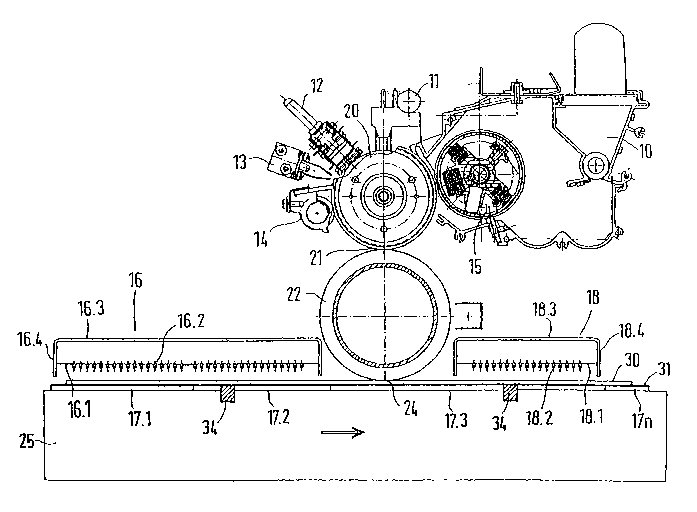
An electrophotographic printing device for plate-shaped substrates 30 is
represented in a lateral view and partially in section in Fig. 1. The
substrate 30 is moved
linearly past a transfer zone 24 of a transfer unit by means of a table-like
transport device 25.
Here, an intermediate layer consisting of an insulator 17, or segments 17.1 to
17.n thereof,
is located between the underside of the substrate 30 and the support surface
of the transport
device. Charging of the substrate 30 takes place via a partial charging device
16 arranged
upstream of the transfer unit in the transporting direction, and a partial
charging device 18,
arranged downstream of the transfer unit, which maintain a number of
electrically conductive
corona wires stretched on non- conductive corona wire holders in housings. The
partial
charging devices 16 and 18 are embodied as area coronas and extend
transversely over the
entire width of at least the substrates 30 to be imprinted.
The top of the insulator plate 17, or of the segments 17.1 to 17.n, facing the
underside of the substrates 30, is provided with a metallic layer 31.
As can be seen from the diagram in Fig. 2, the transport device 25 is
grounded,
i.e. connected with the counter-potential of the charge voltage U~. Therefore
the corona
wires of the partial charging devices 16 and 18 are uniformly connected to the
potential of
the charge voltage U~. The metallic layer 31 of the insulator 17, or of the
segments 17.1 to
8
CA 02458535 2004-02-24
17.n, remains free of potential or, for the further improvement of the toner
transfer, is
charged with a voltage (UF) to ground of 1 to 10 kV, in particular between 3.5
and 5 kV.
The transfer unit is in contact with the substrate 30 in the area of the
transfer
zone for the toner transfer, wherein the transport speed of the substrate 30
is matched or
coupled to the speed of rotation of the transfer unit in such a way that no
slippage occurs
between them.
As can be additionally found in Fig. 1, it is possible to integrate functional
elements 34 into the transport device 25, which are in contact with the
undersides of the
substrates 30 to be imprinted through the insulator 17.
These functional elements 34 can be aspirating openings, grooves, transport
elements, sensors, cable conduits or other components, which preferably are
flush with the
top of the metallic layer 31 and, where required, are maintained with spring
tension against
the underside of the substrate 30 by means of springs 32, as shown in Fig. 3.
In this case the
functional elements 34 can be connected by means of potential balancing lines
33 with the
reference potential of the charge voltage U~ and the metallic layer 31,
however, they are
maintained electrically insulated in the transport direction, as shown by the
small air gap.
Such transport devices 25 can pass one after the other through the transfer
zone and each can
be occupied with one or several substrates 30 to be imprinted.
The parts of an electrophotographic printing device, which per se and in its
functioning is known, will be briefly presented by means of Fig. 1.
A toner, for example a ceramic, a thermoplastic or a duromeric plastic toner
is stored in a developer unit 10. A developer drum 15 is assigned to the
developer unit 10,
9
CA 02458535 2004-02-24
which conducts the toner to a photo-conductor 20. The photo-conductor 20 is
embodied in
a roller shape and is in linear contact with the transfer unit 22 in a contact
zone 21. A coating
unit 11 is arranged above the photo-conductor 20, which exposes a light-
sensitive layer at
the circumference of the photo-conductor 20. A latent electrostatic charge
image is created
by this. Based on the charge image, toner particles are transferred by means
of electrostatic
processes from the developer drum 15 to the layer of the photo-conductor 20.
These toner
particles are passed on to the transfer unit 22 in the area of the contact
zone 21. A cleaning
device 14, which is arranged downstream in respect to the direction of
rotation of the photo-
conductor 20, removes still adhering toner remnants from the photo-conductor
20. A
quenching light 13 follows the cleaning device 14, which discharges the
photosensitive layer
of the photo-conductor 20. Thereafter the photosensitive layer of the photo-
conductor 20 is
again brought to the uniform charge structure, so that it can again be
provided with an
electrostatic charge image by the exposure unit 11.
The transfer unit rolls off on the substrate 30 to be imprinted. In the
process,
the toner on the transfer unit is transferred to the substrate 30 in the
transfer zone. Since the
partial charging devices 16 and 18 cause a full-area charge of the substrate
30 with opposite
potential in respect to the charge on the photo-conductor 20, an unequivocal
toner transfer
with a high degree of effectiveness takes place.
As can be seen in Fig. 1, the distance in the transport direction between the
partial charging devices 16 and 18 is less than the dimension of the substrate
in this direction,
so that it is assured that the substrate 30 remains charged during its entire
passage through
the transfer zone.
CA 02458535 2004-02-24
Fig. 4 represents a transport device 25, which is grounded and has an endless
conveyor belt between two reversing rollers, which belt is itself electrically
conductive and
constitutes the conductive layer 31. The reversing rollers form an insulator
17.3, which can
also be constituted by reversing rollers with an insulating circumferential
layer, for example
a PTFE layer. The base of the reversing rollers can also be made of an
insulating material.
The additional voltage is supplied for example via additional wiper contacts
37.
The endless conveyor belt can be a close-meshed metal belt, which makes the
fixing in place of the substrate 30 easier by means of suction.
Similar to Fig. 2, Fig. 5 shows a grounded transport device 25 with an
insulator
17 arranged on it. The electrically conductive layer 31 between the substrate
30 and the
insulator 17 is charged by means of a field voltage OF to 1 to 10 kV, in
particular between
1.5 and 4 kV. The charging devices 16 and 18, as well as the transfer zone 24
above the
substrate 30 are embodied and arranged the same as in Fig. 2.
As shown in Fig. 6, the substrate 30 can also be received in an insulated mold
35.1 with rims 35.2. This mold can be arranged on an electrically conducting
layer 31, which
is separated via an insulator 17 from the grounded transport device 25, but is
being
transported with it. The receptacle of the mold 35.1 has an electrically
conductive surface
36, which is provided with the field voltage OF by means of wiper contacts 37.
11