Note: Descriptions are shown in the official language in which they were submitted.
CA 02459220 2004-03-O1
IMAGE SENSING APPARATUS
Background of the Invention
The present invention relates to an image sensing apparatus ,
and more particularly to an image sensing apparatus called
"vision chip", which is applied to a vision sensor and image
processing. Here, the "vision chip" signifies, for example,
a visual sensor chip (semiconductor or circuit) in which a
super-parallel circuit structure with optical sensor circuits
and processing circuits arranged for individual pixels is
realized by an analog CMOS integrated circuit, and which can
perform visual information processing. Among such vision chips,
especially a vision chip which simulates the circuit structure
and functions of an organic retina shall be called "silicon
retina".
Shown in Fig. 22 is the schematic constructional view of
a vision chip. A lower view is the enlarged view of the vision
chip 61. As in the enlarged view, each pixel includes an optical
sensor 63 and a processing circuit 64. Image information is
projected on the vision chip 61 through an optical system
constructed of a lens 62, etc. The projected image information
is converted into electric signals by the optical sensors 63,
and the electric signals are processed in super-parallel fashion
by the processing circuits 64 arranged in the respective pixels .
Besides, the processing circuits 64 convert the electric signals
into information which is easily understood by a higher-degree
recognition apparatus such as computer or microprocessor, and
which is outputted.
Owing to such a vision chip, a problem at which a prior-art
image processing system based on a serial type digital computer
1
CA 02459220 2004-03-O1
is inapt can be solved. Various vision chips have heretofore
been developed, and the principal items of visual information
processing incarnated by the vision chips are, for example,
"image smoothing", "contour emphasis" and "motion detection".
Shown in Fig. 23 is the circuit arrangement view of a
single-chip system. Here, a vision chip which performs the
smoothing, contour emphasis and velocity detection of an input
image as one circuit example will be mentioned. In case of the
single-chip system, besides an optical sensor 63, the processing
circuits of a smoothing circuit 65, a contour emphasis circuit
66 and amotion detection circuit 67 must be respectively arranged
in each pixel as shown in the figure.
Summary of the Invention
With the vision chip of the single-chip system as stated
above, however, the optical sensor and the processing circuits
are arranged in each pixel, so that the geometrical structure
(pixel size) of one pixel enlarges inevitably. Moreover, with
the prior-art vision chip, various visual processing functions
need to be incarnated by one chip, so that the number of pixels
per unit area of the chip decreases to degrade a spatial resolution .
Furthermore, with the prior-art vision chip, the pixel size is
made small by simplifying the pixel structure, so that
satisfactory image processing cannot be executed in
higher-degree recognition processing at the posterior stage in
some cases . Besides , when a countermeasure in which the number
of pixels is increased by enlarging a chip size is taken, the
cost of the chip rises ( incidentally, this is also ascribable
to the fact that unusable chips increase with increase in the
number of fabricated chips), and the chip size itself has a
limitation dependent upon a CMOS manufacturing process, from
2
CA 02459220 2004-03-O1
the viewpoint of available percentage.
In view of the above drawbacks , the present invention has
for its object to adopt the construction of a so-called
"multi-chip system" in which grocessing to be executed by one
chip is divided and performed by a plurality of chips, whereby
the various processing steps of image processing ar the like
are performed by a super-parallel circuit structure, and they
are executed in real time. Also, the invention has for its object
to provide a system of low price, small size and low dissipation
power utilizing, for example, CMOS. Further, the invention has
for its object to provide a system having robustness peculiar
to analog devices.
According to the resolution means of the present invention ,
there is provided an image sensing apparatus comprising:
first pixel circuits each of which includes an optical
sensor that converts an inputted light signal into an electric
signal, and a first processing circuit that executes first analog
processing for the output from the optical sensor and outputs
analog image information; and
second pixel circuits each of which includes a second
analog memory that receives the analog image information from
the first processing circuit of said first pixel circuit and
stores the received analog image information, and a second
processing circuit that reads out the image information from
the second analog memory, executes second analog processing and
outputs analog image information, and which is disposed in
correspondence with said first pixel circuit;
wherein the first and second pixel circuits being
respectively arranged in matrix shapes so as to form first and
second chips, and the first and second processing circuits
respectively receiving analog signals from the nearby first and
second processing circuits in the first and second chips
3
CA 02459220 2004-03-O1
corresponding thereto, so as to compensate for characteristics
and to execute the first and second analog processing by parallel
calculations.
Brief Description of the Drawings
Fig . 1 is a constructional view of a pixel sensing apparatus
being a multi-chip system.
Fig. 2 is a block diagram of a type-1 chip.
Fig. 3 is a block diagram of a pixel circuit of Type 1.
Fig. 4 is a block diagram of a type-2 chip.
Fig. 5 is a block diagram of a pixel circuit of Type 2.
Fig. 6 is a timing chart of shift registers for selecting
noticed pixels.
Fig . 7 is an arrangement diagram of the pixel circuit of
one pixel of Type 1.
Fig. 8 is a timing chart concerning the operation of a
pixel level.
Fig. 9 is an arrangement diagram of a resistance network.
Fig. 10 is an explanatory diagram of the image of contour
emphasis based on a unidimensional resistance network.
Fig. 11 is an explanatory diagram of the image of contour
emphasis based on resistance networks of two layers.
Fig. 12 is an arrangement diagram of the pixel circuit
( 2 ) of one pixel of Type 2 .
Fig. 13 is a timing chart concerning the operation of a
pixel level.
Fig. 14 is an explanatory diagram of the image of the
difference between frames.
Fig. 15 is an arrangement diagram of the pixel circuit
(1) of one pixel of Type 2.
Fig. 16 is a timing chart concerning the operation of a
4
CA 02459220 2004-03-O1
pixel level.
Fig. 17 is a constructional view of a mufti-chip system.
Fig. 18 is a view of a binocular stereoscopic system
constructed of mufti-chip systems.
Fig. 19 is a circuit diagram of an active pixel sensor.
Fig. 20 shows a circuit diagram of a noise compensation
buffer, and a timing chart of control signals.
Fig . 21 shows a circuit diagram and an explanatory diagram
of a resistance network.
Fig. 22 is a schematic constructional view of a vision
chip.
Fig. 23 is a circuit arrangement view of a single-chip
system.
Detailed Description of Preferred Embodiments of the Invention
1. Mufti-chip system
Shown in Fig. 1 is the constructional view of an image
sensing apparatusbeing a mufti-chipsystem. In this embodiment,
by way of example, the three processing items of smoothing,
contour emphasis and motion detection are respectively
distributed to three chips, which are constructed into a
mufti-chip. The smoothing chip 1 of first stage, to which image
information is inputted from an optical system 4 constructed
of a lens, etc., includes an optical sensor circuit 1-1, and
a smoothing circuit 1-2 which is a processing circuit for
smoothing, thereby to smooth an input image. The smoothed image
information is outputted as voltage ox current analog signals
from the first-stage smoothing chip 1, and the analog signals
are inputted to the contour emphasis chip 2 and motion detection
chip 3 of second stage, et seq. The pixels of the contour emphasis
5
CA 02459220 2004-03-O1
chip 2 and motion detention chip 3 at the second stage, et seq.
include analog memories 2-1, 3-1, and a contour emphasis circuit
2-2 and a motion detection circuit 3-2 which are dedicated
processing circuits, respectively. The analog memories 2-1,
3-1 temporarily store the analog information fram the preceding
stages, respectively. The contour emphasis circuit 2-2 and
motion detection circuit 2-3 read the information of the analog
memories 2-1, 3-1 (if necessary, they are also capable of writing
information), respectively. Here, contour-emphasized image
information items are outputted from the second-stage contour
emphasis chip 2, while motion-detected results are outputted
from the third-stage motion detection chip 3.
As the features of such a multi-chip system, the following
points, for example, are mentioned:
~ Processing which is performed by one chip can be limited
(processing functions can be distributed).
~ A pixel size is small.
~ The number of pixels can be increased without enlarging a chip
size.
~ Since outputs are delivered in parallel from a plurality of
chips, high-degree image processing which utilizes a plurality
of visual information items can be executed.
~ A compensation circuit is easily arranged in each pixel in
order to remove circuit noise which is added in image processing
and data transfer.
~ Analog information is employed for image processing and the
transfer of data. Besides, the image processing can be executed
at high speed by a super-parallel circuit structure which is
based on analog processing circuitsarranged in individual pixels.
This goint is clearly different from the operation of any existing
DSP (Digital Signal Processor) for image processing.
Here, the differences between the present invention and
6
CA 02459220 2004-03-O1
the DSP will be described.
In case of the DSP, image information outputted from
imaging equipment such as a CCD camera is converted by an A/D
converter into digital signals, which are sent to the DSP, and
digital image processing is executed by the DSP . In contrast ,
in case of the embodiment of the present invention, at the stage
of the first-stage smoothing chip 1, image information is
initially acquired and is simultaneously subjected to
super-parallel analog image processing by the analog processing
circuits of the individual pixels (point of difference from the
CCD camera). Subsequently, computed analog information items
are directly outputted from the first-stage smoothing chip 1
and are inputted to the contour emphasis chip 2 of the next stage
(A/D conversion is not performed). Subsequently, the
information items from the first-stage smoothing chip 1 are
inputted to the analog memories arrayed in the respective pixels
of the next-stage contour emphasis chip 2 and are further
subjected to super-parallel processing by the analog processing
circuits of the respective pixels (point of difference from
digital image processing) . Besides, information items from the
contour emphasis chip 2 are inputted to the analog memories
arrayed in the respective pixels of the next-stage motion
detection chip 3 and are further subjected to super-parallel
processing by the analog processing circuits of the respective
pixels.
In general, a processing circuit can be designed on a
smaller scale in an analog circuit than in a digital circuit .
Assuming that DSPs be arranged in individual pixels with the
intention of performing parallel image calculations, there are
such problems as follows:
~ A pixel size becomes large.
~ Wiring for connecting respective pixels becomes complicated.
7
CA 02459220 2004-03-O1
In contrast, according to the present invention, these problems
are relieved for the reason that the respective pixels are
constructed of analog circuits.
As a problem peculiar to an analog integrated circuit,
however, the influence of dispersion ascribable to the
non-uniformity of element characteristics is supposed in some
cases. This signifies that, even when circuits being
geometrically quite the same are designed within an identical
chip, the electrical characteristics of the individual circuits
become discrepant. In addition to the discrepancy appearing
within the chip, the tendency appears more intensely among
separate chips. The dispersion of the element characteristics
among the respective pixels in the super-parallel circuit
structure as in the present invention, and the change of the
information items of the preceding and succeeding chigs in the
case of the transfer of image information to the next stage need
to take countermeasures when they are serious.
In the present invention, therefore, the problem is solved
in such a way that a circuit which compensates for the dispersion
( circuit noise ) attendant upon the non-uniformity of the element
characteristics is incorporated in each pixel. In the
compensation circuit, the circuit noise of the corresponding
pixel is stored in a certain sort of analog information storage
element , thereby to incarnate image processing and data transfer
which are not influenced by the circuit noise. Concretely, a
noise compensation buffer circuit (to be explained later) is
supposed, but any circuit having a similar function can be
substituted therefor.
2. Outline of Circuit arrangement of Chips constituting
Multi-chip system
8
CA 02459220 2004-03-O1
The sorts of chips constituting a multi-chip system are
broadly divided into the following two types in the embodiment
of the present invention:
~ Type 1: an optical sensor for acquiring image information,
and a processing circuit are built in each pixel
~ Type 2: an analog memory for storing image information from
a preceding stage, and a processing circuit are built in each
pixel
Circuit arrangements will be described on the types 1 and
2.
( 1 ) Circuit arrangement of Type-1 chip ( Image acquisition
+ Parallel image processing)
The chip of Type 1 is at the first stage of the chip system
to-be-constructed, and it acquires the image information items
of the outside world by the optical sensors built in the respective
pixels and subjects the acquired information items to image
processing in parallel.
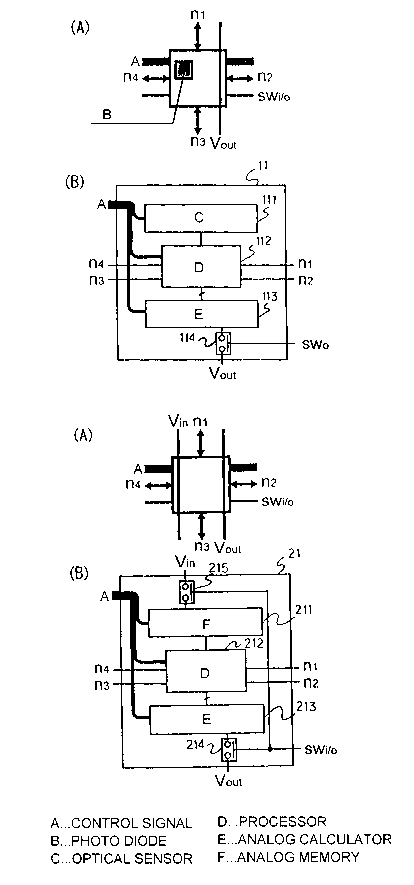
Shown in Fig . 2 is the block diagram of the type-1 chip .
The type-1 chip includes pixel circuits 11, a horizontal
shift register 13, a vertical shift register 14, switches 15,
an outputting buffer 16, and an output line 17. The pixel
circuits 11 are sequentially selected by the horizontal shift
register 13 and the vertical shift register 14, so as to read
out outputs calculated in parallel. (Incidentally, the timing
chart of the shift registers will be explained later.)
Shown in Fig. 3 is the block diagram of the pixel circuit
of Type 1. The pixel circuit 11 includes an optical sensor 111,
a processing portion 112 , an analog calculator 113 , and a switch
114 . The roles of the respective constituents will be described
below.
The optical sensor 111 converts an optical signal ( image
9
CA 02459220 2004-03-O1
information ) into an electric signal such as voltage or current .
Used as a circuit element therefor is any of a photodiode, a
phototransistor, an active pixel sensor, etc. The processing
portion 112 receives an input from the optical sensor 111 of
its own pixel circuit, and inputs n1 - n4 from the nearby pixel
circuits, and it performs image processing. This processing
portion 112 chiefly performs parallel image calculations which
employ the information items of the nearby pixels. The analog
calculation portion 113 receives inputs from the processing
portion 112, and performs an analog calculation conforming to
the four rules of arithmetic, or the like. This analog
calculation portion 113 may well simultaneously include a circuit
which compensates for circuit noise ascribable to the dispersion
of the characteristics of the individual elements, the circuit
noise being a problem that is to be dealt with in an analog
integrated circuit. The output of the analog calculation
portion 113 becomes a pixel output . In this embodiment , a control
signal for the pixel circuits 11 is inputted to all the pixels
collectively, but it may well be inputted every pixel circuit
or every row or column.
( 2 ) Circuit arrangement of Type- 2 chip ( Analog memory +
Parallel image processing)
The chip of Type 2 is at the second or subsequent stage
of the chip system to-be-constructed, and it stores image
information items delivered from the preceding stage, in the
analog memories built in the respective pixels, and subjects
the delivered information items to image processing in parallel
by the processing circuits arranged in the respective pixels .
Shown in Fig. 4 is the block diagram of the type-2 chip.
The type-2 chip includes pixel circuits 21, a horizontal
shift register 23, a vertical shift register 24, switches 25,
an inputting buffer 26, an output line 27, an input line 28,
CA 02459220 2004-03-O1
and an outputting buffer 29. Noticed pixels are sequentially
selected by the horizontal shift register 23 and the vertical
shift register 24, so as to input data from the chip of the
preceding stage to the pixel circuits 21 and to read out outputs
calculated in parallel. (Incidentally, the timing chart of the
shift registers will be explained later.)
Shown in Fig . 5 is the block arrangement of the pixel circuit
of Type 2.
The pixel circuit 21 is constructed of an analog memory
211, a processing portion 212, an analog calculator 213, and
it includes switches 114, 115. The roles of the respective
constituents will be described below.
The analog memory 211 stores image information inputted
from outside (in this case, the pixel circuit of Type 1, the
pixel circuit of Type 2 at the preceding stage , or the like ) .
The processing portion 212 receives an input from the analog
memory 211 of its own pixel circuit, and inputs n1 - n4 from
the nearby pixel circuits, and it performs image processing.
This processing portion 212 chiefly performs parallel image
calculations which employ the information items of the nearby
pixels . The analog calculation portion 213 receives inputs from
the processing portion 212, and performs an analog calculation
conforming to the four rules of arithmetic, or the like. This
analog calculation portion 213 may well simultaneously include
a circuit which compensates for circuit noise ascribable to the
dispersion of the characteristics of the individual elements ,
the circuit noise being a problem that is to be dealt with in
an analog integrated circuit. The output of the analog
calculation portion 213 becomes a pixel output. In this
embodiment , a control signal for the pixel circuits is inputted
to all the pixels collectively, but it may well be inputted every
pixel circuit or every row or column.
11
CA 02459220 2004-03-O1
Next, shown in Fig. 6 is the timing chart of the shift
registers for selecting noticed pixels.
In both the chips of Types 1 and 2 , the horizontal shift
registers 13 , 23 and the vertical shift registers 14 , 24 select
noticed pixel circuits to/from which image information items
are inputted/outputted. The basic timings of the shift
registers become as shown in the figure. In the chip of Type
2, the row of a pixel array is selected by the vertical shift
register 24, and the input/output switch SWi/o of the selected
pixels is connected to the input/output lines of the respective
columns. In this state, the input/output lines of one set are
selected by the horizontal shift register 23 and the switch 25,
and they are respectively connected to the input buffer 26 and
the output buffer 29. That is, the input buffer 26 and the output
buffer 29 are connected to the pixel selected by the row and
the column. A situation in the case of Type 1 is similar, but
the path of an input is unnecessary.
3. Circuit examples of Chips
( 1 ) Circuit example of Type-1 chip: Image acquisition + Smoothing
Shown in Fig . 7 is the arrangement diagram of the pixel
circuit of one pixel of Type 1.
This pixel circuit includes an optical sensor 111, a
processing portion 112, an analog calculator 113, and a switch
114. In this example, the optical sensor 111 is made an APS
(active pixel sensor: to be explained later) , which accumulates
light charges and thereby converts a light signal into voltage
information. The processing portion 112 is constructed of a
resistance network here. Image information is inputted to the
resistance network, whereby an input image can be smoothed in
super-parallel fashion (as will be explained later). The
12
CA 02459220 2004-03-O1
resistance network is formed by having resistance-based
connections ( n1 , n2 , n3 , n4 ) with nearby pixels , so as to smooth
the input image. An output from the processing portion 112 is
inputted to the analog calculator 113. The analog calculator
113 employs a noise compensation buffer circuit Nbuf: to be
explained later. The noise compensation buffer circuit Nbuf
can compensate for the dispersion of the circuits on the input
side and the offset of an amplifier within this noise compensation
buffer circuit Nbuf, in accordance with control signals. A
switch SWo is controlled by the horizontal shift register 13
and the vertical shift register 14, whereby a noticed pixel can
be selected to read out data.
Shown in Fig. 8 is a timing chart concerning the operation
of a pixel level. Now, operations will be described as to
individual intervals.
Interval (A) : A control signal SWp for the switch of the
APS is asserted to "H" , thereby to initialize the APS . Thereof ter ,
the control signal SWp is negated to "L" , thereby to shift to
a charge accumulating operation in the APS for the nth frame.
Intervals (B) + (C): Accumulation time of the APS
Interval (C): With the lapse of the accumulation time,
a control signal SWh is asserted to "H" , thereby to connect the
resistance network of the processing portion 112 and the noise
compensation buffer circuit Nbuf . On this occasion, the output
Vnet of the resistance network becomes:
Vnet = Vnet(n)+VN1 (1)
Here, Vnet(n) denotes image information processed by the
resistance network, and VN1 denotes circuit noise at this time.
Control signals SW1 and SW2 are controlled in this state, whereby
the output of the resistance network as expressed by Eq. (1)
is stored in a capacitance built in the noise compensation buffer
circuit Nbuf.
13
CA 02459220 2004-03-O1
Interval (A' ) : The control signal SWp for the switch of
the APS is asserted to "H" again, thereby to initialize the APS.
On this occasion, the output Vnet of the resistance network
becomes:
Vnet = VnetO +VNO (2)
Here, VnetO denotes an initial voltage from the resistance
network at the initialization of the APS, and VNO denotes circuit
noise at the initialization. That is, an input voltage to the
noise compensation buffer circuit Nbuf has changed from Eq. ( 1 )
to Eq. (2). On this occasion, assuming that the magnitude of
the circuit noise be always constant ( VN1 = VNO ) , an output Vout
from the noise compensation buffer circuit Nbuf becomes:
Vout(n)=Vnet(n)-VnetO+VN1-VNO+Vref
=Vnet(n)-VnetO +Vref
so that the output which is proportional to processed information
in the resistance network as is free from the influence of the
circuit noise is obtained. Thereafter, the control signal SWh
is asserted to "H", whereby the output is held in the noise
compensation buffer circuit Nbuf. Besides, the control signal
SWp is negated to "L" , thereby to shift to a charge accumulating
operation in the APS for the (n + 1)th frame.
Interval (B'): Since the APS and the circuit Nbuf are
electrically isolated, the output Vout(n) can be read out by
closing an output switch signal SWo, in parallel with the
accumulating operation in the APS for the (n + 1)th frame.
The acquisition of image information and the smoothing
operations based on the resistance networks can be performed
by repeating the above operations.
(2) Circuit example 1 of Type-2 chip: Contour emphasis
Shown in Fig. 9 is the arrangement diagram of a resistance
network.
14
CA 02459220 2004-03-O1
A network in which pixels are coupled by resistances as
in the figure, is called the "resistance network". Owing to
the resistance network, an input image can be smoothed (as will
be explained later) . The differential output between the input
image and a smoothed image emphasizes the contour of the input
image.
Shown in Fig. 10 is the explanatory diagram of the image
of contour emphasis based on a unidimensional resistance network .
The axis of abscissas in Diagram (A) represents a pixel
No. , while the axis of ordinates represents corresponding pixel
information (voltage ) . An input Vk whose voltage value changes
greatly at the 0th pixel, is applied to the resistance network.
This corresponds to the contour of an image. On this occasion,
a signal Vlk with a contour part smoothed is outputted from the
resistance network. It is in Diagram (B) that the differential
output between the signals Vk and Vlk has been taken. It is
seen that a great response is exhibited at the 0th pixel being
the position of the contour, and that, around the 0th pixel,
the voltage gradually comes to take a constant value with a
distance from the position of the contour. That is, the contour
part is emphasized.
Besides, shown in Fig. 11 is the explanatory diagram of
the image of contour emphasis based on resistance networks of
two layers.
When image information smoothed by another resistance
network beforehand as stated above is employed as the input of
a resistance network, that is, when resistance networks are used
in two layers, an output as in the figure is obtained. It is
known that the characteristics of the filter approximate
Laplacian-Gaussian (~2G) mathematically, and the smoothing of
an input image and the emphasis of a contour can be simultaneously
performed. Moreover, the filter is excellent for removing
CA 02459220 2004-03-O1
spatial image noise at high frequencies.
Shown in Fig . 12 is the arrangement diagram of the pixel
circuit (2) of one pixel of Type 2.
This pixel circuit includes an analog memory 211, a
processing portion 212 , an analog calculator 213 , and switches
214, 215. The analog memory 211 stores external image
information in a capacitor built therein. The processing
portion 212 is constructed of a resistance network. This
processing portion 212 forms the resistance network by having
resistance-based connections(nl,n2,n3,n4)with nearby pixels,
so as to smooth an input image . Both an input to and an output
from the processing portion 212 are outputted to the analog
calculator 213 . A noise compensation buffer circuit Nbuf ( to
be explained later) is employed as the analog calculator 213.
The noise compensation buffer circuit Nbuf can compensate for
the dispersion of the circuits on the input side and the offset
of an amplifier within this noise compensation buffer circuit
Nbuf , in accordance with control signals . Signals SWi, SWo are
controlled by the horizontal shift register 23 and the vertical
shift register 24, whereby a noticed pixel can be selected.
Shown in Fig. 13 is a timing chart concerning the operation
of a pixel level. Although one layer of the resistance network
will be exemplified here, two layers may well be employed as
stated above . Now, operations will be described as to individual
intervals.
Interval (A) : An input control signal SWi from the shift
register is asserted to "H", thereby to store external image
information (Vin(n)) in the analog memory 211.
Interval (B): The control signal SWh of a data holding
switch and the control signal SWs of an input changeover switch
are asserted to "H" , thereby to connect the noise compensation
buffer circuit Nbuf and an input V1 from the analog memory 211.
16
- CA 02459220 2004-03-O1
The switching operations of the control signals SW1, SW2 of the
noise compensation buffer circuit Nbuf are performed in this
state, whereby the input V1 from the analog memory 211 is stored
in the noise compensation buffer circuit Nbuf . Simultaneously,
the dispersion of the input side of the circuit and the offset
of the amplifier within the noise compensation buffer circuit
Nbuf are compensated for (noise compensation operation).
Interval (C): The control signal SWs of the changeover
switch is negated to "L", thereby to connect the noise
compensation buffer circuit Nbuf and the output V2 of the
resistance network, so that the following computation is executed
in the noise compensation buffer circuit Nbuf:
Vout(n)= V2(n)-V1(n)+Vref
That is, an output which is proportional to the difference between
the input image information V1 ( n ) and the smoothed output V2 ( n )
from the resistance network is obtained.
Interval ( D ) : The control signal SWh of the data holding
switch is negated to "L" , whereby the computed image information
is held in the noise compensation buffer circuit Nbuf.
Interval (A' ) : An output control signal SWo from the shift
register is asserted to "H" , thereby to read out the output Vout ( n )
held in the noise compensation buffer circuit Nbuf.
Simultaneously therewith, the input control signal SWi from the
shift register is asserted to "H", whereby image information
( Vin ( n+1 ) ) at the next time is stored in the analog memory 211.
Thenceforth, similar operations are repeated, whereby a
contour-emphasized output can be delivered.
(3) Circuit example 2 of Type-2 chip: Motion detection
Shown in Fig. 14 is the explanatory diagram of the image
of the difference between frames .
It is assumed that, in the image of the certain nth frame,
17
CA 02459220 2004-03-O1
a black disc have been entered in a white ground (Diagram (A) ) .
It is supposed that the black disc have moved rightwards in the
image of the ( n + 1 ) th frame ( Diagram ( B ) ) . I t is as sumed that
the image outputs of the nth and (n + 1)th frames be voltage
values, and the potential difference between these outputs is
computed. Then, only the part of the movement responds as in
Diagram (C). In this manner, the motion of an object can be
computed by computing the difference between the frames.
Shown in Fig . 15 is the arrangement diagram of the pixel
circuit (1) of one pixel of Type 2.
This pixel circuit includes an analog memory 211, an analog
calculator 213 , and switches 214 , 215 . The analog memory 211
stores external image information in a capacitor built therein.
A noise compensation buffer circuit Nbuf ( : to be explained later )
is employed as the analog calculator 213 . The noise compensation
buffer circuit Nbuf can compensate for the dispersion of the
circuits on the input side and the offset of an amplifier within
this noise compensation buffer circuit Nbuf, in accordance with
control signals. Signals SWi, SWo are controlled by the
horizontal shift register 23 and the vertical shift register
24, whereby a noticed pixel can be selected.
Shown in Fig. 16 is a timing chart concerning the operation
of a pixel level. Now, operations will be described as to
individual intervals.
Initial condition: A signal SWh is always held at an "H"
input , thereby to connect the analog memory 211 and the noise
compensation buffer circuit Nbuf.
Interval ( A ) : A pixel value ( Vin ( n ) ) on the analog memory
211 is stored in the noise compensation buffer circuit Nbuf by
the switching operations of the control signals SW1, SW2 of this
noise compensation buffer circuit Nbuf. Simultaneously, the
dispersion of the input side of the circuit and the offset of
18
CA 02459220 2004-03-O1
the amplifier within the noise compensation buffer circuit Nbuf
are compensated for (noise compensation operation).
Interval ( B ) : An input control signal SWi from the shif t
register is asserted to "H" , whereby the information of the analog
memory 211 is updated to information at the next time (Vin(n
+ 1)). Simultaneously, the following computation is executed
in the noise compensation buffer circuit Nbuf:
Vout = Vin(n) - Vin(n+1) + Vref
That is , an output which is proportional to the difference between
the pixel information at the current time (n + 1) and the pixel
information at the last time (n) is obtained. An output control
signal SWo is asserted to "H" , thereby to read out the output
of the noise compensation buffer circuit Nbuf.
Interval (A'): The switching operations of the control
signals SW1, SW2 are performed again, whereby pixel information
(Vin(n + 1)) on the analog memory 211 is stored in the noise
compensation buffer circuit Nbuf, and the noise compensation
operation is performed by the noise compensation buffer circuit
Nbuf.
Thenceforth, similar operations are repeated, whereby the
differential output between frames can be delivered.
4. Constructional examples of Multi-chip systems
Shown in Fig. 17 is an example of the constructional view
of a multi-chip system.
Here, the following chips mentioned as the chip circuit
examples above are constructed in the form of the multi-chip
system:
~ Image acquisition + smoothing chip 1
~ Contour emphasis chip 2
~ Motion detection chip 3
19
CA 02459220 2004-03-O1
Here will be described a circuit example in which the image
acquisition + smoothing chip 1, the contour emphasis chip 2 and
the motion detection chip 3 are connected in series in this order.
First, the acquisition of an input image and the smoothing
of the input image are performed in the smoothing chip 1 of the
initial stage. When the image of an apple has been projected
on the smoothing chip 1 as shown in Diagram ( A ) , an output in
which spatial noise components contained in the image are
smoothed is obtained.
The output of the initial-stage smoothing chip 1 is
inputted to the contour emphasis chip 2 of the second stage.
Since contour emphasis processing with the smoothed image is
executed in the second-stage contour emphasis chip 2, a filter
of Laplacian-Gaussian type is formed, and an output in which
the smoothing and contour emphasis of the input image are done
is obtained. It is understood that, as shown in Diagram (B) ,
feature quantities such as the contour of the apple and the strings
of leaves are emphasized.
The output of the second-stage contour emphasis chip 2
is inputted to the motion detection chip 3 of the third stage.
A part where the image with the contour of the input image
emphasized has moved, can be detected in the third-stage motion
detection chip 3. When the apple has horizontally moved
rightwards , it is understood that , as in Diagram ( C ) , the output
of the contour in the direction in which the apple moves appears
low ( in black ) , whereas the output of the contour on the opposite
side appears high ( in white ) , almost no response being exhibited
in the vertical direction in which the apple does not move.
Owing to such construction of the chip system, the
"smoothed image","contour-emphasized image"and"motion image"
can be outputted in parallel.
Next, shown in Fig. 18 is an example of the constructional
CA 02459220 2004-03-O1
viewof abinocular stereoscopic system constructed of multi-chip
systems.
Even a complicated image processing system such as of
binocular stereoscopy can be coped with by preparing two chips
51, 52 of Type 1 for acquiring images as shown in the figure.
The outputs of the two type-1 chips 51, 52 are inputted
to a plurality of visual function chips 53, 54, 55, 56 so as
to derive visual information items in parallel. Thereafter,
the information items are bound. This permits to precisely and
quickly solve the corresponding point problem at which a general
serial image processing system is inapt.
Here, the visual function chips 53, 56 function as the
motion detection chips stated above, and the visual function
chips 54, 55 function as the contour emphasis chips stated above.
Besides, a visual function chip 57 applies the motion detection
chip and receives the outputs of the two visual function chips
54 , 55 , thereby to have the function of detecting the difference
of the outputs.
5. Circuit examples
Shown in Fig. 19 is an example of the circuit diagram of
an active pixel sensor.
In this example, a photosensor is used in a charge
accumulating mode, and a source-follower circuit is added to
the output node of the photosensor, thereby to construct the
active pixel sensor (APS) . Since the output of the photosensor
lowers to the amount of the threshold voltage of MOS at
initialization, a PMOS source follower (PSF) is employed as the
source-follower circuit.
Shown in Fig. 20 are examples of the circuit diagram of
a noise compensation buffer and the timing chart of control
21
CA 02459220 2004-03-O1
signals.
A noise compensation buffer circuit is a circuit in which
circuit noise ascribable to the dispersion of elements is stored
in a built-in capacitance, thereby to compensate for the circuit
noise (refer to T. Sibano, K. Iizuka, M. Miyamoto, M. Osaka,
R. Miyama and A. Kito: "Matched Filter for DS-CDMA of up to
50MChip/s Based on Sampled Analog Signal Processing", ISSCC
Digest of Tech. Papers, pp. 100-101, Feb. 1997).
Operations will be described in con junction with the timing
chart of control signals in the figure.
[1] (SW1: ON, SW2: connected to ref)
On this occasion, input V(in) - VinO + VNO
(here, VinO: initial value of an input signal from a circuit
at a preceding stage, VNO: circuit noise of the preceding stage)
Voltage of the inverting node of an AMP,
V ( in- ) - V ( ref ) + Voff
(here, Voff: offset voltage of the AMP)
Charges accumulated in the inverting node of the AMP,
Q= C1 ( V(ref) + Voff - VinO - VNO )
+ C2 ( V(ref) + Voff - V(ref) ) (3)
[2] (SW1: OFF, SW2: connected to ref)
On this occasion, the inverting node of the AMP falls into
a floating state, and the charges are held as they are. (An
operation till here is called the "reset operation".)
[3] (SW1: OFF, SW2: connected to the output of the AMP)
On this occasion, the input changes to V(in) = Vinl + VN1
( here , Vinl : input signal from the circuit at the preceding stage,
VN1: circuit noise of the preceding stage at the input of the
signal Vinl)
Charges accumulated in the inverting node of the AMP,
Q= C1 ( V(ref) + Voff - Vinl - VN1 )
+ C2 ( V(ref) + Voff - V(out) ) (4)
22
CA 02459220 2004-03-O1
From Eqs. (3) and (4),
V(out) - - ( C1/C2 )( Vin1 - VinO + VN1 - VNO )
+ V(ref)
Accordingly, if the circuit noise in the preceding-stage
circuit is constant ( VNO = VN1 ) , the output V ( out ) is free from
the influence of , not only the of f set of the AMP of the compensation
buffer circuit itself , but also the circuit noise of the preceding
stage, and it becomes proportional to the variation of the input
voltage.
Incidentally, the operating region of the noise
compensation buffer circuit depends upon the operating region
of the AMP employed. The operating regions for the respective
AMPs used are as follows:
~ Transconductance amplifier (AMP1): Operating for the minus
change of the input
~ Transconductance amplifier (AMP2): Operating for the plus
change of the input
~ Wide-range amplifier: Operating for both the plus and minus
changes of the input
Shown in Fig. 21 are the circuit diagram and explanatory
diagram of a resistance network.
Super-parallel image calculationsbased on the resistance
network will be described with reference to this figure (refer
to C. Mead: "Analog VLSI and Neural Systems" , Addision-Wesley,
Reading, MA, 1989, and T. Yagi, S. Ohshima and Y. Funahashi:
"The role of retinal bipolar cell in early vision: an implication
with analogue networksand regularizationtheory",Biol.Cybern,
77, pp. 163-171, 1997) . The distribution of the output voltages
of the resistance network becomes the input voltages thereof
as smoothed. In a case where the number of nodes is sufficiently
large, the voltage distribution in the resistance network can
be considered as stated below.
23
CA 02459220 2004-03-O1
The voltage distribution will be explained in con junction
with the schematic diagram of the resistance network in Diagram
(A).
It is assumed that the input voltage at k = 0 be Vk = VO ,
and that the other input voltages be zero ( spatial impulse input ) .
The response potential Vlk of the resistance network to this
input becomes:
V1k - BiVoYi~k~ Equation 1
Here , Bi - 1 / 4L12 + 1 Li = R" / F~
'~ 1 - ~ + ~ ~( ~12~ - 1 ~ Li 2 + ~ ~~ ~14~
This equation represents that the output signal attenuates
exponentially with a distance from the signal source (k = 0 ) .
Besides, L1 is called the "spatial constant of the
resistance network", and thesignal propagates more extensively
as the numerical value of the spatial constant L1 is larger.
Shown in Diagram ( B ) are results obtained in such a way
that the outgut voltage distribution at the spatial impulse input
was computed for two sorts of spatial constants . A solid line
corresponds to L1 = J(10/6), while a broken line corresponds
to x(1011). Both the results smoothly attenuate exponentially
with the distance from the signal source. It is also understood
that the output propagates more extensively in the broken line
of the larger spatial constant.
A response to any desired input potential distribution
Vi is expressed by the spatial convolution integral of a response
in the case of putting Vk = 1 in Equation 1 and the distribution
Vi, as follows:
Vik - BI,~ Vi'~l~k i
That is, in case of utilizing the resistance network as
a constituent circuit for image processing,
~ it can execute the smoothing processing of an input image at
24
CA 02459220 2004-03-O1
10
high speed in super-parallel fashion by arraying optical sensors
or pixel memories in an input portion, and
~ it can freely regulate a region to-be-smoothed by constructing
resistance elements out of variable resistances.
Industrial Applicability
As described above, the present invention adopts the
construction of a so-called "multi-chip system" in which
processing intended to be executed by one chip is divided and
performed by a plurality of chips , whereby the various processing
steps of image processing or the like are performed by a
super-parallel circuit structure, and they can be executed in
real time. Moreover, according to the present invention, a
system of low price, small size and low dissipation power, which
utilizes CMOS by way of example can be provided. Furthermore,
according to the present invention, a system which has robustness
peculiar to analog devices can be provided.