Note: Descriptions are shown in the official language in which they were submitted.
CA 02459970 2010-09-20
FAULT TOLERANT LED DISPLAY DES ION7
CROSS-- REFEIRFTW t TO RELATED PPLICAT `NS
application is related tV a~aj ,.,.3:I3t s.= .~ .E_._t:_1' as a
cor ti.,iua ^n ,n.-part of J. Patent Application Serial No.
09/675,152 euivA..led ENHANCED T R I M RESOLUTION
DIMMING LE DRIVER and filed Septc;r_. ar 29, 2000, now U.S. Paten"',,
No. 6,323,598, as is ' reA.a to the bj-*-'ot i:.{ .. A. oa`
commonly assigned, :^o...)-.C1.::. C U.S. Patent Application Serial No.
1 10 09/949,131 entitled VOWACE U1"_4FiA%E S LEV DISPLAY PRODUCING
U E COLOK:, . d filed September 7, 2001, U f'a`C-._? ,=i' '`tiSs,
,_ now t:
i 7 .
TECHNICAL FIELD OF 171F, 1x1-. VF :v'" (}
The present invention is directed, in ger-teral, to driver
cir= ul v.. for light emitting diode _ :::_ m nation : ux-ceS. and,
20 More npe?c:L icailY to voltage-controlled dium.,d?:#g r. 1"JC
Circus t,,. for light emit.t:i.ng diode Wkumin,ation
of providing i:llumat:iots despite failure of One or '7:..r...
emitting th.a&!s w thii the w 1...Lum.inat on ouT:ce.
CA 02459970 2004-03-05
WO 03/024159 PCT/IB02/03585
2
BACKGROUND OF THE INVENTION
Commercial and military aircraft instrumentation
displays, like many other display systems, frequently employ
illuminated indicators and controls. Traditionally,
incandescent lamps operating at 5 VAC, 14 VDC or 28 VDC have
been employed as illumination sources for illuminated push-
button switches, indicators and annunciators within aircraft
instrumentation. The illumination from such incandescent
lamps is generally optically filtered to produce a wide range
of human visible or night vision imaging system (NVIS) colors,
and the small size of incandescent lamps allows multiple lamps
to be used within the same display to illuminate different
regions of the display in different colors.
The inherent characteristics of incandescent lamps,
however, lead to noticeable chromaticity shifts as the applied
voltage is reduced to adjust the output luminance from
sunlight readability in daytime flying conditions to low
luminance levels required for night flying conditions.
Moreover, incandescent lamps suffer other disadvantages when
employed in aircraft instrumentation, including high power
consumption, high inrush current, uncomfortably high touch
temperatures, and unreliability in high vibration
environments. As a result, considerable effort has been
expended to incorporate more stable, efficient and reliable
technologies, such as light emitting diodes (LEDs), into
aircraft crewstation illuminated displays. Light emitting
diodes offer high luminous efficiency, low heat, low power
consumption and high reliability.
The luminance required for aircraft instrumentation
displays ranges up to approximately 400-500 foot-lamberts for
CA 02459970 2004-03-05
WO 03/024159 PCT/IB02/03585
3
sunlight-readability in daytime flying. In order to provide
sufficient illumination to be visible in direct sunlight,
multiple light emitting diodes may be required. For example,
FIGURES 3A and 3B depict circuit diagrams for driver
configurations which might be employed in light emitting diode
illumination sources for aircraft instrumentation. Drivers
300 and 301 each include a biasing resistor R2 and a set of
light emitting diodes Ll-L4 connected in series between input
and output ports ("+" and "-") to which the input voltage is
applied. In driver 300, the light emitting diodes L1-L4 are
connected in parallel. Unfortunately, the power consumption
of parallel light emitting diodes increases linearly with each
additional light emitting diode, and can even consume as much
power as the incandescent lamps which the light emitting diode
illumination sources are designed to replace.
By connecting the light emitting diodes Ll-L4 in series,
as in driver 301, maximum power efficiency can be realized.
Since current is constant in series-connected light emitting
diodes, the power consumed by a display containing multiple
series-connected light emitting diodes is no more than that
consumed by a display containing only a single light emitting
diode, while the total luminance increases with each light
emitting diode added.
In a series-connected configuration such as driver 301,
however, if any of light emitting diodes Ll-L4 fails in an
electrically open state, the entire string of light emitting
diodes is rendered nonfunctional.
There is, therefore, a need in the art for a light
emitting diode illumination source providing both power
efficiency and fault tolerance for failure of one or more
light emitting diodes in an electrically open condition.
CA 02459970 2004-03-05
WO 03/024159 PCT/IB02/03585
4
SUMMARY OF THE INVENTION
To address the above-discussed deficiencies of the prior
art, it is a primary object of the present invention to
provide, for use in a light emitting diode illumination
source, a fault tolerance for failure of one light emitting
diode within a series-connected group. In the present
invention, such fault tolerance is provided by a zener diode
connected in parallel with sets of series-connected light
emitting diodes with a reverse forward bias orientation. The
threshold voltage of the zener diode is matched to equal, or
be just slightly greater than, the forward voltage drops for
the light emitting diodes at maximum current. During normal
operation, therefore, the zener diode draws virtually no
current. Upon failure of one of the light emitting diodes,
the zener diode conducts without increase in the applied
voltage, providing an alternate current path maintaining
circuit integrity so that other sets of light emitting diodes
connected in series within the circuit continue to illuminate.
The foregoing has outlined rather broadly the features
and technical advantages of the present invention so that
those skilled in the art may better understand the detailed
description of the invention that follows. Additional
features and advantages of the invention will be described
hereinafter that form the subject of the claims of the
invention. Those skilled in the art will appreciate that they
may readily use the conception and the specific embodiment
disclosed as a basis for modifying or designing other
structures for carrying out the same purposes of the present
invention. Those skilled in the art will also realize that
CA 02459970 2004-03-05
WO 03/024159 PCT/IB02/03585
such equivalent constructions do not depart from the spirit
and scope of the invention in its broadest form.
Before undertaking the DETAILED DESCRIPTION OF THE
INVENTION below, it may be advantageous to set forth
5 definitions of certain words or phrases used throughout this
patent document: the terms "include" and "comprise," as well
as derivatives thereof, mean inclusion without limitation; the
term "or" is inclusive, meaning and/or; the phrases
"associated with" and "associated therewith," as well as
derivatives thereof, may mean to include, be included within,
interconnect with, contain, be contained within, connect to or
with, couple to or with, be communicable with, cooperate with,
interleave, juxtapose, be proximate to, be bound to or with,
have, have a property of, or the like; and the term
"controller" means any device, system or part thereof that
controls at least one operation, whether such a device is
implemented in hardware, firmware, software or some
combination of at least two of the same. It should be noted
that the functionality associated with any particular
controller may be centralized or distributed, whether locally
or remotely. Definitions for certain words and phrases are
provided throughout this patent document, and those of
ordinary skill in the art will understand that such
definitions apply in many, if not most, instances to prior as
well as future uses of such defined words and phrases.
CA 02459970 2004-03-05
WO 03/024159 PCT/IB02/03585
6
BRIEF DESCRIPTION OF THE DRAWINGS
For a more complete understanding of the present
invention, and the advantages thereof, reference is now made
to the following descriptions taken in conjunction with the
accompanying drawings, wherein like numbers designate like
objects, and in which:
FIGURES lA and 1B depict circuit diagrams for fault
tolerant light emitting diode driver circuits according to
various embodiments of the present invention;
FIGURE 2 is a circuit diagram for a fault tolerant
voltage-controlled dimming light emitting diode driver
according to another embodiment of the present invention; and
FIGURES 3A-3B are circuit diagrams for simple light
emitting diode drivers.
CA 02459970 2004-03-05
WO 03/024159 PCT/IB02/03585
7
DETAILED DESCRIPTION OF THE INVENTION
FIGURES 1A, 1B and 2, discussed below, and the various
embodiments used to describe the principles of the present
invention in this patent document are by way of illustration
only and should not be construed in any way to limit the scope
of the invention. Those skilled in the art will understand
that the principles of the present invention may be
implemented in any suitably arranged device.
FIGURES 1A and 1B depict circuit diagrams for fault
tolerant light emitting diode driver circuits according to
various embodiments of the present invention. Drivers 100 and
101 each include a biasing resistor R2 and a set of series-
connected light emitting diodes Ll-L4 connected in series
between input and output ports ("+" and "-") to which the
input voltage is applied. In order to realize the power
savings of series-connected light-emitting diodes with the
catastrophic loss of the entire set of light emitting diodes
L1-L4 should a single light emitting diode within the set fail
in an electrically open state, zener diodes Z1-Z4 are
connected in parallel with each light emitting diode Ll-L4.
Zener diodes Z1-Z4 have a forward bias orientation
opposite that of the corresponding light emitting diode Ll-L4-
-i.e., the anode of each zener diode Z1-Z4 is connected to the
cathode of the corresponding light emitting diode L1-L4 while
the cathode of each zener diode Z1-Z4 is connected to the
anode of the corresponding light emitting diode Ll-L4. Zener
diodes Z1-Z4 provide an alternate current path if the
counterpart light emitting diode L1-L4 fails in an
electrically open state, maintaining circuit integrity so that
CA 02459970 2004-03-05
WO 03/024159 PCT/IB02/03585
8
the remaining light emitting diodes can continue to
illuminate.
To reduce the number of components, a single zener diode
may be connected in parallel with two or more light emitting
diodes, providing a route-around current path bypassing a
failed light emitting diode (and other light emitting diodes
in the same group around which the zener diode is connected)
to render the circuit fault tolerant. FIGURE 1B depicts a
circuit diagram for a variant driver 101 in which zener diodes
Z1-Z2 are each connected in parallel with a pair of light
emitting diodes Ll/L2 and L3/L4.
The reverse breakdown threshold voltage of each zener
diode should preferably be selected to be just slightly
greater than or equal to the maximum forward bias voltage
drop(s) (i.e., the forward voltage drop at maximum current)
across the light emitting diode(s) for which the zener diode
provides a circuit bypass. In such cases, the zener diode
will draw virtually no current in normal operation, but will
not require a substantial increase in the applied input
voltage to activate the route-around current path in the event
a parallel light emitting diode fails.
The design of FIGURE 1B, where each zener diode is
connected in parallel around two light emitting diodes, is
therefore preferred. Should any light emitting diode Ll-L4 in
the series-connected circuit suffer a failure, the primary
current path will revert through one of the zener diodes Z1-Z2
without requiring an increase in the applied input voltage,
retaining illumination of at least one-half of the light
emitting diodes. More complex configurations involving active
switching circuits may also be employed if desired to provide
additional fault tolerance, or fault tolerance which is better
CA 02459970 2004-03-05
WO 03/024159 PCT/IB02/03585
9
matched to the forward voltage drops of the light emitting
diodes.
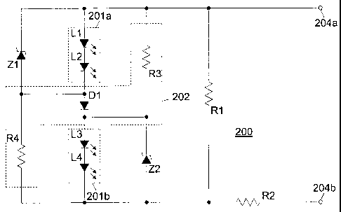
FIGURE 2 is a circuit diagram for a fault tolerant
voltage-controlled dimming light emitting diode driver
according to another embodiment of the present invention.
Circuit 200 includes four white light emitting diodes L1-L4
series-connected in pairs L1/L2 and L3/L4 within two LED
groups 201a and 201b. A switching circuit 202 is connected
between LED groups 201a and 201b to switch LED groups 201a and
201b from series-connection between input and output ports
204a and 204b to parallel-connection, or vice-versa, as the
voltage applied across input and output ports 204a-204b is
varied across a threshold or "kickover" value.
Switching circuit 202 includes a switching diode D1
connected in series between LED groups 201a and 201b, a first
resistor R3 connected in parallel with both LED group 201a and
switching diode D1, and a second resistor R4 connected in
parallel with both LED group 201b and switching diode D1.
The cathode of switching diode Di is connected to the
anode of the last light emitting diode L2 (in the direction of
the forward voltage drop across the LEDs) within LED group
201a and to one end of resistor R4; the anode of switching
diode D1 is connected to the cathode of the first light
emitting diode L3 with LED group 201b and to one end of
resistor R3. An opposite end of resistor R3 is connected to
the cathode of the first light emitting diode Li within LED
group 201a, and an opposite end of resistor R4 is connected to
the anode of the last light emitting diode L4 within LED group
201b.
LED groups 201a and 201b (comprising light emitting diode
pairs Ll/L2 and L3/L4) are connected by switching circuit 202
CA 02459970 2004-03-05
WO 03/024159 PCT/IB02/03585
either in series or in parallel between input and output ports
204a-204b, depending on the voltage applied across the input
and output ports 204a-204b. Switching circuit 202 provides
kickover from parallel-connection to series-connection, and
5 vice-versa, of LED groups 201a-201b. Switching diode D1 and
resistors R3 and R4 enable the switching mechanism.
In operation, circuit 200 operates in two modes: high
luminance mode above the kickover point, where the applied
input voltage across ports 204a-204b is greater than the
10 combined forward voltage drops (turn-on voltages) of light
emitting diodes L1-L4 and switching diode D1; and low
luminance mode below the kickover point, where the applied
input voltage across ports 204a-204b is less than the combined
forward voltage drops of light emitting diodes L1-L4 and
switching diode D1 (but greater than the combined forward
voltage drops of either of light emitting diode pairs ll/L2 or
L3/L4).
In high luminance mode, switching diode Dl conducts, and
most of the current between ports 204a-204b passes through the
series connected path of light emitting diode pair L1/L2,
switching diode D1, and light emitting diode L3/L4. The
primary current path for high luminance control is established
by the high luminance resistor R2.
In low luminance mode, switching diode D1 stops
conducting and the current passes through the two parallel
paths comprising: light emitting diode pair Ll/L2 and
resistor R4; and resistor R3 and light emitting diode pair
L3/L4. Low luminance mode therefore results when the applied
input voltage is insufficient to allow forward current to flow
through switching diode D1. The primary current path for low
CA 02459970 2004-03-05
WO 03/024159 PCT/IB02/03585
11
luminance control is established by low luminance resistors
R3-R4.
Resistor R1 provides a quiescent current path to prevent
false or unintentional illumination at low current levels,
which otherwise may produce detectable illumination at levels
of as low as a few microamperes (pA) . In addition to setting
the kickover point as a function of input voltage applied
across ports 204a-204b, resistor R2 serves to limit the
current of a transient or overvoltage event and also serves to
limit the operating current to safe levels in order to prevent
a catastrophic failure of the display circuitry.
Zener diodes Z1 and Z2, in conjunction with high
luminance resistor R2, provide circuit protection against
transients, conducted electromagnetic susceptibility, or an
electrostatic discharge event. Zener diodes Z1 and Z2 also
prevent failure of the entire set of light emitting diodes L1-
L4 should a single light emitting diode Ll-L4 fail in an
electrically open state, providing an alternate current path
to maintain circuit integrity with two light emitting diodes
still illuminating under such a catastrophic failure
condition.
Exemplary values for the relevant components depicted in
FIGURE 2 are: resistor R1 = 4.32 kiloohms (Ku); resistor R2 =
1.5 KS2; resistors R3 and R4 = 20 KQ; light emitting diodes Li-
14 each having forward voltage drops in the range 2.5-3.3 VDC;
and zener diodes Z1-Z2 are rated for about 6.6 VDC.
Within light emitting diode illumination sources, the
present invention obtains the power efficiency benefits of
series-connecting light emitting diodes while avoiding
complete failure of the illumination source should a single
light emitting diode fail in an electrically open state. By
CA 02459970 2004-03-05
WO 03/024159 PCT/IB02/03585
12
matching the threshold voltage of the zener diode to the
forward voltage drops of one or more series-connected light
emitting diodes connected in parallel with the zener diode,
current draw by the zener diode during normal operation is
kept to essentially zero while an alternate current path is
activated upon failure of a light emitting diode without
increasing the applied voltage.
Although the present invention has been described in
detail, those skilled in the art will understand that various
changes, substitutions, variations, enhancements, nuances,
gradations, lesser forms, alterations, revisions, improvements
and knock-offs of the invention disclosed herein may be made
without departing from the spirit and scope of the invention
it its broadest form.