Note: Descriptions are shown in the official language in which they were submitted.
CA 02460153 2006-06-05
1
DIRECTIONAL COUPLER
BACKGROUND OF THE INVENTION
The invention relates to a directional coupler.
A directional coupler has been disclosed, for example,
in DE 23 20 458 C2. This comprises an asymmetric
stripline and a coaxial line, and the stripline in this
directional coupler is coupled to the coaxial inner
conductor. The strip conductor is in this case fitted
in the coupling zone into an exposed cutout in the
outer conductor of the coaxial line, with the ground
conductor of the stripline at the same time forming the
shield (which is interrupted by the cutout) of the
coaxial line.
A directional coupler which is to this extent
comparable to this prior art has also been disclosed in
DE 199 28 943 Al. In order to provide inductive
coupling as well in a directional coupler such as this,
this prior publication proposes that the base plate be
in the form of a circular substrate wafer which is
seated in an appropriately cylindrical milled-out area.
The angle of the substrate wafer can thus be rotated
with the coupling piece.
The directional coupler can thus be tuned by rotating
the coupling line in the electromagnetic coaxial cable
field. However, the tuning is in this case restricted
just to the coupling loss. The achievement of a high
degree of directionality, as is of major importance in
practice, plays no role in this solution.
The directional coupling signal variables which are
tapped off in the cited prior art are supplied in a
known manner to an external evaluation device, to be
CA 02460153 2006-06-05
2
prEcise via coaxial cables. Since radio-frequency
signals are emitted, high-quality and costly coaxial
cables must therefore also be used, in the same way as
high-quality and costly coaxial plug connectors as
well, of course. The aim of this is to ensure that a
high-quality connection and thus good directionality
can also be achieved, with respect to the
characteristic impedance.
Equally, only comparatively poor directionality levels
can be achieved with the known directional couplers.
Against the background of the prior art in this field,
the object of the present invention is thus to provide
an improved directional coupler which allows better
signal values to be achieved with the design whose cost
is lower overall.
BRIEF SUMMARY OF THE INVENTION
In accordance with the object of the invention, there is provided a
directional
coupler having at least one coupling line piece which is coupled to a coaxial
inner conductor of coaxial line pieces and, for this purpose, the coupling
line
piece is provided on or adjacent to a coupler substrate which is arranged on a
resting or mounting section of an outer conductor of the coaxial line piece in
the
region of a cutout in the outer conductor, and the coupling line piece is in
this
way held in a space between the inner conductor and the outer conductor,
comprising:
- an attenuation circuit adjacent and connected to each of the two
coupling line ends on the coupler substrate, or an attenuation circuit
connected to one coupling line end with a terminating resistor being
connected to the other coupling line end on the coupler substrate,
CA 02460153 2009-01-12
2a
- an electrical level evaluation circuit device provided on the coupler
substrate, and
- an interface device for connection of unshielded cables provided on the
coupler substrate, or unshielded cables connected to the level evaluation
circuit device or connected downstream from the level evaluation circuit
device on the coupler substrate, via which the RF signals which are
obtained via the coupling line piece can be passed on in the form of analog
AF signals.
In contrast to the prior art in its entirety, the
invention now proposes that an attenuation circuit be
provided on the base plate of the directional coupler,
adjacent to each of the two ends of the coupling piece,
or that an attenuation circuit be provided at one end
of the coupling piece with a terminating resistor being
provided at the other end of the coupling piece. If a
terminating resistor is provided at one end of the
coupling piece, then this is a so-called single-armed
directional coupler, in which the second coupling arm
is terminated by the terminating resistor.
CA 02460153 2004-03-09
- 3 -
However, electronic level evaluation is provided, in
particular, on the directional coupler itself, that is
to say preferably on the base plate. An interface
device is also fitted, to which, however, only one
unshielded cable can then be connected - since the
radio-frequency signal processing takes place on the
directional coupler itself. Specifically, a flat ribbon
cable is preferably connected to this interface device
and, of course, this can be provided at a considerably
lower cost than high-quality coaxial cable connections.
Th-is configuration according to the invention not only
results in major cost advantages over conventional
solutions, but also results in considerably better
directionality values!
The advantages according to the invention are
particularly major when an attenuation circuit is
provided at each of the two ends of the coupling piece
on the base plate of the directional coupler. This is
because this makes it possible to use the signals in
both directions on the output line further, or to
process them further (double coupler) . If one side of
the output line is in contrast terminated by a
terminating resistance, then only one signal path can
be evaluated. This would mean that a separate coupler
would be required in each case for the forward path and
return path. If one directional coupler were in each
case used for each direction (that is to say one for
the forward path and one for the return path), the
directionality levels would have to be set separately
for each path, which would make two separate couplers
necessary (twice the adjustment complexity). In
consequence, integration on a common printed circuit
board would also be impossible, and the evaluation
electronics would have to be provided on a third
printed circuit board. This would then in turn
necessitate the connection between the coupler and the
third printed circuit board having to be implemented
CA 02460153 2004-03-09
- 4 -
using high-quality, and thus very expensive, radio-
frequency coaxial lines. This is avoided with the
solution according to the invention.
In one preferred embodiment of the invention, a II
circuit, which is known per se, or, for example, a T
circuit using appropriate resistors is used for the
attenuation elements. In particular, these circuit
arrangements can be fitted without any problems to the
base plate or to the directional coupler.
The forward path and return path on a printed circuit
board can be produced particularly easily by using a rI
attenuation element or by using a T attenuation
element, as a result of which the evaluation
electronics can be integrated on the printed circuit
board with a high level of integration. Since the
coupling piece is installed accurately, the directional
coupler is highly directional. If multilayer material
is used, the achievable directionality of the coupler
is improved even further. In addition, this also allows
the integration density to be increased further.
Furthermore, filter modules may also be accommodated on
the respective arm of the directional coupler.
It has also been found to be particularly advantageous
for a level detector to be accommodated on the
directional coupler, that is to say in particular on
the base plate.
Finally, one development of the invention proposes that
a nonvolatile EEPROM memory module also be located on
the directional coupler, and that this be used to store
the transfer function of at least one, and preferably
both coupling arms together with an electronic
evaluation. This now ensures a unique association
between the RF level value that is present and the
resultant detector voltage. All the component
CA 02460153 2006-06-05
tolerances for the directional coupler and the
evaluation electronics are thus combined and stored in
a common assembly. Furthermore, this also makes it
considerably easier to replace individual assemblies in
a unit. This is because, in the coupler systems which
have already been disclosed, it was in contrast
necessary either to carry out complex matching on the
overall unit after replacement of individual
components, or to use very high-quality, narrow-
tolerance individual components, whose interaction did
not require any matching.
BRIEF DESCRIPTION OF THE DRAWINGS
The invention will be explained in more detail in the
following text with reference to drawings in which, in
detail:
Figure 1: shows a schematic perspective [sic]
illustration of a coaxial conductor with
a connecting region for the directional
coupler;
Figure 2: shows a schematic vertical sectional
illustration through the base plate of
the directional coupler and of the
coaxial conductor;
Figure 3: shows a schematic plan view of the
illustration shown in Figure 2;
Figure 4: shows an enlarged detailed illustration
of the base plate, which comprises the
coupling piece as well as the electronic
assemblies and components, of the
directional coupler including an
extension section;
CA 02460153 2006-06-05
6
Figure 5: shows a schematic circuit diagram to
illustrate the electronics that are
located on the base plate; and
Figure 6: shows a circuit arrangement, modified
from that shown in Figure 5, for a
single-armed directional coupler, in
which one output of the directional
coupler is connected via a terminating
resistor, and an attenuation element in
the form of a T is provided instead of
an attenuation element in the form of a
II at the other output.
DESCRIPTION OF THE PREFERRED EMBODIMENTS
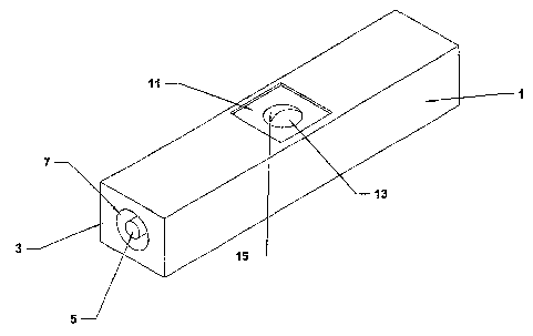
Figures 1 et seq. show a directional coupler which
comprises a continuous coaxial line piece 1 with an
outer conductor 3, which is illustrated in a
perspective [sic] view and has a relatively bulky form
in Figure 1, and with an inner conductor 5.
In the illustrated exemplary embodiment, the outer
conductor 3 has a square or rectangular external
diameter [sic]. The inner conductor 5, which is
cylindrical in the illustrated exemplary embodiment, is
provided such that it runs electrically isolated from
the outer conductor 3, forming a hollow-cylindrical
separation area 7 in the interior of the outer
conductor 3.
As can be seen in particular in Figure 1, a resting or
mounting section 11, preferably in the form of a
depression or a milled-out area, is provided on the
outer conductor 3. An exposed cutout 15, that is to say
a window 15, is provided in the wall of the outer
conductor 3 in a coupling zone 13 that is formed in
this way.
CA 02460153 2006-06-05
6a
The coupler 19 together with the coupler substrate 19'
is then firmly mounted on the outer conductor 3 in this
coupling zone 13, for example by means of two or more
screws 16 located in laterally offset positions with
respect to the exposed cutout 15, with a coupling line
CA 02460153 2004-03-09
- 7 -
piece 23 being provided on the lower face of the
coupler substrate 19'. In this case, the coupling line
preferably has a length of <k/4, in particular a
length of > X/16, and_especially around X/8. For this
purpose, appropriate threaded holes are incorporated in
the wall of the outer conductor 3 at the points at
which the screws 16 are located, and are aligned with
corresponding holes 18 in the coupler substrate 19' in
order to screw in the appropriate screws 16.
The coupling line piece 23 may be provided in a
predetermined alignment on the coupler substrate 19',
to be precise so as to achieve coupling loss levels
that are advantageous base on experience.
The coupling line piece 23 may, for example, be formed
from a stripline. However, a wire clip or a wired
component (resistor) may be used just as well.
The coupler substrate 19' is in the form of a
multilayer structure whose shielding surface offers
good shielding, thus resulting in a coupler which is
resistant to interference radiation overall. The
multilayer structure 19' thus once again completely
closes the shield for the coaxial line, which is
interrupted by the exposed cutout 15.
The signals which are tapped off on the coupling line
piece 23 in the relevant electromagnetic field are
passed via through-plated holes to the upper face of
the coupler, where the electronic components are
located which convert the emitted RF signals directly
to analog AF voltages for further processing.
For this purpose, attenuation elements or attenuation
circuits 27 of suitable size are provided immediately
adjacent to the coupling line ends 25, are used for
forced matching for the coupling line at both ends and
CA 02460153 2004-03-09
- $ -
thus fundamentally also govern the directionality of
the coupler.
In the exemplary embodiment illustrated in Figure 5,
the attenuation circuit 27 is in this case in the form
of a 11 circuit, in which a first resistor R1 is in each
case connected in the signal line 29, and two further
resistors R2 and R3, respectively, which are connected
to ground or to an opposing potential, are connected
upstream and downstream of the resistor R1.
As is also shown in Figure 6, an attenuation circuit in
the form of a T can be used instead of an attenuation
circuit 27 in the form of a II such as this, in which
two resistors R4 and R5 are connected in series in the
signal line 29, and a resistor R6 which is connected to
ground or to an opposing potential is connected between
them.
Alternatively, other attenuation circuits are in
principle feasible (for example fixed attenuation
elements).
As can be seen from the exemplary embodiment
illustrated in Figure 5, the electronic RF components
for the upper face of the coupling are chosen and
arranged so that they are identical and symmetrical for
both coupling arms. Since any disturbance influences
such as mismatches, component tolerances and
temperature drifts act equally on both coupling arms,
these influences cancel one another out.
The plan view in Figure 5 also shows that a filter 31
as well as a level detector 33, for example, and an
EEPROM 37 can also be accommodated in the two coupling
arms A, B downstream from the attenuation circuits 27,
with the transfer function of the two coupling arms
together with an electronic evaluation preferably being
stored in the EEPROM memory module.
CA 02460153 2004-03-09
- 9 -
The entire arrangement, including an interface device
35, can be accommodated on the coupling substrate 19'.
If the central section 19a of the coupling conductor
substrate 19' is not large enough for the electronic
components, then the coupler substrate 19' may also
have an extension section 19b, which projects further
at the sides, in addition to the central section 19a
which is located immediately above the free cutout 15
on the outer conductor 3 of the coaxial line piece 1
(Figure 4 ) .
A mating plug device or contact device 36 can now be
connected by means of an unshielded cable to said
interface device 35, in order to tap off the analog
signals, for example an unshielded ribbon cable 41,
which leads to an externally accommodated
microprocessor module 43.
In the illustrated exemplary embodiment, the coupler
substrate 19' is a multilayer substrate with four
layers, so that it is possible to produce a combination
of an RF directional coupler and electronic evaluation
on a single compact assembly. In this case, there are
two internal layers, with the lower internal layer
being used as a reference ground for the coupling line
piece. However, the layer structure of the coupler
substrate may also be configured differently, for
example with a different substrate thickness or number
of layers. The printed circuit board substrate may
change for each layer, and may thus also have different
quality levels and price classes.
Figure 6 will be used firstly to show that the
attenuation elements 27 may also be in the form of the
T circuit that has been mentioned. Furthermore,
Figure 6 illustrates a directional coupler which has
only one arm. In this case, the one coupling arm on the
CA 02460153 2004-03-09
- 10 -
coupler substrate 19' is terminated by a terminating
resistor 49.
In addition to the exemplary embodiments which have
been explained, it should be noted that both the length
and the width of the coupling line piece can be varied,
and it may also in this case be mounted in a different
relative position, that is to say in particular a
different rotation position with respect to the inner
conductor located underneath. In this case, the
coupling line piece need not be in the form of a
stripline. In fact, it may also be a wire clip, or may
be in the form of a wired component (resistor).
As has already been indicated, the position and the
configuration of the coupler substrate may be formed
differently to the position and configuration in the
illustrated exemplary embodiments. For example,
different substrate thicknesses or a coupler substrate
with a different position and a different number of
layers from those in the illustrated exemplary
embodiment can thus be used.
Finally, the printed circuit board substrate may also
be formed from different quality levels and price
classes.
As can be seen in particular by reference to Figures 4
and 5, the electrical and electronic components may be
fitted not only on the upper face of the coupler, that
is to say the upper face of the coupler substrate 191,
but also on the lower face. Finally, the assemblies
which have been described may also include elements for
temperature compensation which allow, for example,
software or hardware temperature compensation.
Furthermore, in addition to absolute level information,
the assembly on the coupler substrate may also supply
difference values for the level and phase between the
CA 02460153 2004-03-09
- 11 -
two coupling arms. These signals can also be evaluated
appropriately, and can be made available to a
downstream microprocessor via the flat ribbon cable.
Finally, the two coupling arms a and b can be evaluated
via separate or common electronic paths 29. Frequency-
governing elements such as bandpass filters 31 or
bandstop filters can be implemented in the evaluation
paths, *in order to suppress interference frequencies.
Finally, an additional circuit or a microprocessor may
also be provided on the assembly, to evaluate the
detector voltages obtained and, derived from them, to
produce variables such as the reflection factor, return
loss or standing wave ratio (VSWR). It may be necessary
for the coupler substrate to be larger or to have a
larger coupling attachment 19b.