Note: Descriptions are shown in the official language in which they were submitted.
CA 02460577 2004-03-10
MATERIAL SEPARATION TO FORM SEGMENTED PRODUCT
Technical Field
This invention relates to material handling and particularly to separation of
one material
from another wherein the separated material is segmented to subsequently mate
with another
component for a specific purpose. In one example, the separated segmented
material may form
an adhesive-type layer to bond various electronic components such as a heat
sink to a chip, an
electronic package stiffener to a circuitized substrate such as a printed
circuit board (PCB), etc.
Background of the Invention
Material separation of several different types of materials is, of course,
well known in the
art of materials handling. The same is true for separation of materials having
openings, slots, etc.
therein. One example that comes readily to mind is gasket material for such
products as
manufacturing equipment, automobiles, etc. As will be defined herein, the
present invention is
particularly directed (but not limited) to the separation of segmented
materials for eventual use in
electronic products such as electronic packages, several types of which are
known in the
electronic field. Examples are shown and described in the following U.S.
Patents:
5,106,451 - Kan et al
5,726,079 - Johnson
6,288,900 - Johnson et al
An electronic package sold by the assignee of this invention is of particular
interest. It is
sold under the name HyperBGA , the "BGA" standing for ball (e.g., solder) grid
array meaning
a pattern of solder balls are used to bond the package to a selected
underlying substrate, typically
a laminate PCB. (HyperBGA is a registered trademark of Endicott Interconnect
Technologies,
Inc., the assignee of the present invention.) This particular package also
utilizes a pattern of
solder balls to couple the package's chip to its own substrate body, thus
affording a more dense
package than wirebond or the like packages also on the market. Significantly,
the HyperBGA
package also preferably includes what is referred to as a "stiffener" to add
rigidity to the final
EI-2-03-003 1
CA 02460577 2004-03-10
structure by bonding the package's substrate (a laminate) to a heat sink
spacedly positioned
above the substrate for cooling of the chip during package operation. Further
description of this
particular electronic package will be provided hereinbelow.
Although the invention defined herein is not meant to be limited for use with
electronic
packages such as described above, it is particularly useful in such
applications, especially to
bond one or more elements of the aforementioned HyperBGA package to form the
rigidized
structure needed. The segmented material product separated in accordance with
the unique
teachings herein can be formed in a new and unique manner resulting in
significant cost savings
to the ultimate package consumer.
It is believed that a method for forming a segmented material offering the
advantageous
features taught herein, especially in the electronic packaging field, would
constitute a significant
advancement in the art.
Objects and Summary of the Invention
It is a primary object of the invention to enhance the materials handling art.
It is another object of the invention to provide an improved method of
separating a
particular layer of material from another so as to facilitate subsequent
utilization thereof with
other components, e.g., so as to effectively bond such components.
It is still another object of the invention to provide such a method which can
be
accomplished in a facile and less expensive manner than similar methods of
material separation
known in the materials handling art.
These and other objects are achieved according to one aspect of the invention
by the
provision of a method comprising the steps of providing a layer of base
material, positioning a
layer of first material and a layer of release material on the layer of base
material such that the
layer of release material is located substantially between the layer of base
material and the layer
EI-2-03-003 2
CA 02460577 2004-03-10
of first material, providing a plurality of first cuts substantially only with
the layer of first
material, providing a plurality of deeper second cuts substantially only
within the layer of release
material and the layer of first material, and separating the layer of the
first material from the
layer of base material so as to remove only selected portions of the first
material and leave other
portions of the first material on the layer of base material.
Brief Description of the Drawings
1
FIG. 1 is a side elevational view, in section, of a material which, when cut
as taught
herein, can be effectively separated from another material in accordance with
the teachings
herein;
FIG. 2 is a side elevational view, in section, showing the material of FIG. I
positioned
on a layer of base material, including a third material located therebetween;
FIG. 3 is a side elevational view, in section, illustrating representative
cuts of selected
parts of the materials illustrated therein;
FIG. 4 is a top, partial plan view of part of the structure of FIG. 3,
illustrating the various
portions thereof that can be individually separated in accordance with the
teachings herein;
FIG. 5 is a side, elevational view, in section (although the 3-layered
structure in FIG. 1 is
shown as a single layer), depicting the peel away removal of portions of the
layer of first material
in FIG. I and of the underlying interim (release) layer between it and the
underlying base layer
of material;
FIG. 6 illustrates a side view, in elevation, of an electronic package which
includes
elements that can be assembled using the separated material of FIG. 5; and
FIG. 7 illustrates an information handling system, e.g., a computer server,
which can
utilize one or more of the electronic packages formed using the separated
material formed in
accordance with the method taught herein.
EI-2-03-003 3
CA 02460577 2011-03-21
Best Mode for Carrying Out The Invention
For a better understanding of the present invention, together with other and
further
objects, advantages and capabilities thereof, reference is made to the
following disclosure and
appended claims in connection with the above-described drawings. It is
understood that like
numerals will be used to indicate like elements from FIG. 1 to FIG. 7
As stated above, the separated materials formed herein are useful in many
applications
but one in particular is in the field of electronic packaging. Examples of
such packages are
known in the electronic field and examples are provided above. Such packages,
typically
mounted on an electrically coupled to a circuitized substrate such as a PCB
are then usually
mounted within a larger electronic system such as a computer, mainframe,
server, etc. if utilized
in the information handling systems field. By the term "information handling
system" as used
herein shall mean any instrumentality or aggregate of instrumentalities
primarily designed to
compute, classify, process, transmit, receive, retrieve, originate, switch,
store, display, manifest,
measure, detect, record, reproduce, handle or utilize any form of information,
intelligence or data
for business, scientific, control or other purposes. Examples include the
aforementioned
personal computers and larger processors such as servers, mainframes, etc. It
must be
emphasized, however, that the materials formed in accordance with the
teachings herein are not
limited to such usages, and it is well within the powers of one of ordinary
skill in the art to
realize that the invention has many additional and distinctly different uses.
For ease of
description, however, definition of the invention will be with respect to its
eventual use within an
electronic package and further within an information handling system.
4
CA 02460577 2004-03-10
In FIG. 1 there is shown one example of a first material 10 which may be
formed in a
segmented manner having portions thereof selectively removed according to a
specific design,
according to one embodiment of the invention. It is understood that the
invention is not limited
to this material but can be readily used to provide substantially any similar
materials in which
selected openings, slots, grooves, etc. are desired in the final product. In
the embodiment of FIG.
1, first material 10 is shown as including a layer of dielectric, polymeric
material 11 having on
opposite sides thereof respective layers of adhesive 13 and 15 respectively.
In a preferred
embodiment of the invention, material 10 is a recognized flexible circuit
material constructed of
Kapton polyimide film (11), presently commercially available from E.I. duPont
de Nemours
under the product name Pyralux. (Pyralux is a registered trademark of duPont.)
In a preferred
example, the specific Pyralux is known as Pyralux HT, although other versions
of this known
product are possible. Pyralux HT is available in polyimide film thicknesses
from about 0.5 mil
to 5 mils and the corresponding adhesive thickness for each layer 13 and 15
within the range of
about 0.5 mil to about 3 mils. In its simplest form, Pyralux may be provided
with only one side
coated with the desired adhesive (a proprietary, flame-retardant, B-staged
acrylic epoxy). The
invention is not limited to this specific material, however, in that other
insulative-adhesive
material combinations are readily possible for the eventual use of this
product in the manner
taught herein.
As will be described hereinbelow, first material 10 may be used to bond a heat
sink to a
semiconductor chip in an electronic package or find other uses within this
environment, e.g., to
bond a stiffener or other component occasionally used in such packaging.
Further description
will be provided with the description of FIG. 6 below.
Typically, materials such as Pyralux when used in the environment defined
herein have
been relatively difficult to handle, including specifically when cutting and
otherwise forming the
openings and the external peripheral walls thereof, which, as understood, must
be precisely
defined if used in relatively small products such as micro-miniature and the
like electronic
packages. The present invention overcomes these problems while providing a
method which can
be accomplished in a relatively facile manner.
EI-2-03-003 5
CA 02460577 2004-03-10
In FIG. 2, the layer of first material 10 is shown as being positioned on the
layer of base
material 17 with an interim layer of release material 19 located therebetween.
This formation is
attained by a laminating material 19 to material 10 at a temperature of about
100 degrees
Celsius(C) and pressure of about 50 p.s.i. This is sufficient to bond the two
layers for the
purposes herein. First material 10 is not shown in cross-sectional
configuration for ease of
illustration. The preferred release material is also a polymer, Mylar, and
with a Pyralux material
having dimensions as mentioned above, preferably has a thickness of from about
one mil to
about three mils. Mylar is a known polyester film material available on the
market in various
sizes and thicknesses. The layer of base material 17 may, in some conditions,
be considered to
act as a stiffener or support structure to add rigidity to the final assembly
shown in FIG. 2 to
enhance the subsequent cutting operations defined below. Substantially any
support material of
dielectric material or the like may be utilized for base material 17, with a
preferred material also
being sold by duPont under the registered trademark Tyvek. Tyvek is a tough,
durable sheet
material made of high density polyethylene fibers which combines the best
properties of paper,
film and cloth. It is water-resistant, light weight, particulate free, opaque
and resistant to
chemicals, abrasions and aging. In one example, the Tyvek material possessed a
thickness
within the range of from about two mils to about ten mils.
As defined hereinbelow, the method of this invention results in the formation
of desired
cuts within the first material 10 such that this material can then be removed
from the base
material 17 and utilized as desired. As removed, the first material 10 will
include desired
openings (see FIG. 4) therein and possess a final external peripheral shape
desired for mating
with the corresponding structure to which it will bond.
In FIG. 3, a series of cutting operations are performed to provide the
aforementioned
segmented layer of base material. In FIG. 3, at least two different cuts are
provided within the
subassembly comprised of base material 17, release layer 19 and first material
10. These cuts are
provided by a laser, and specifically an ultraviolet (UV) laser. During these
cuts, material 17 is
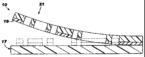
held in contact with material 19 using vacuum. Comparing FIGS. 3 and 4
(illustrating a plurality
of subassemblies of the type shown in FIG. 3 all integrally formed on a
singular, large sheet 21),
EI-2-03-003 6
CA 02460577 2011-03-21
a series of first cuts Cl are provided and a second series of deeper cuts C2
provided. These are
illustrated in phantom in FIG. 3 and also shown in the plan view, but on a
smaller scale, in FIG.
4. The first partial cuts Cl penetrate entirely through the Pyralux layer and
may partly penetrate
the underlying release layer. In comparison, the deeper, second cuts C2
entirely penetrate both
the Pyralux and the release layer 19 but not the support layer of Tyvek. It is
understood that
partial penetration of the Tyvek 10 can and may occur while still achieving
the desired results of
this invention. The first series of cuts Cl were preferably performed for each
of the sections 22
(FIG. 4) at a laser pulse energy of about 0.05 milli joules to 0.15 milli
joules, a pulse spacing of
about 5 micrometers to 15 micrometers, and from about 5 to about 10 passes to
achieve the
desired depth. In comparison, the corresponding series of deeper cuts C2 for
each section were
performed at a laser pulse energy of about 0.07 milli joules to 0.2 milli
joules, a pulse spacing of
about 2 micrometers to 10 micrometers, and from about 5 to about 10 passes to
achieve the
desired depth.
Laser cutting is known in the cutting art, with examples being shown and
described in the
following U.S. patent numbers:
5,138,131 Nishikawa et al
5,565,120 La Rocca
5,578,229 Barnekov et al
5,667,707 Klingel et at
5,688,418 Yoshiyasu et al
5,922,225 Blake
6,313,432B I Nagata et al
6,376,798B I Remue et al
6,476,348B I Grimes
Further description of this process, except to indicate various laser
processing parameters
usable for examples of the invention as noted herein, is not believed
necessary.
7
CA 02460577 2004-03-10
As understood from the illustration in FIG. 4, the full cuts through the
Pyralux and
release sheet illustrated by the designators C2 define a plurality of
rectangular openings within
each respective section 22 of the four sections (three only partially shown)
of layer 21 as shown.
In one embodiment of the invention, a total of 168 individual sections were
formed on one
singular large sheet 21, each section having a width dimension of about 40
millimeters (mm) and
length dimension of 40 mm. The overall sheet possessed length and width
dimensions of 520
mm and 635 mm, respectively. Each section, when removed, will represent a
segmented product
for future use as taught herein. The narrower depth cuts Cl shown in FIG. 4
define the
peripheral sides of these sections for those sides not already cut as defined
by the sheet's external
sidewalls.
In FIG. 5, there is shown the step of separation of part of the segmented
first material 10
and attached release layer 19 from the underlying, supporting base material
17. (In FIG. 5, the
Pyralux material is shown in cross-section as a singular layer of dielectric
for simplification
purposes but it is understood that this material preferably comprises the
dielectric and two
opposing adhesive layers as shown in FIG. 1. Significantly, by virtue of the
differential laser
cutting performed in the manner taught herein, only segmented portions of the
first material are
stripped away, leaving the entirely cut portions defined by cuts C2 still
attached to base material
17. These remaining segments are shown in phantom for ease of illustration.
However, the
removed material is shown in cross-section with these segments removed. The
preferred
separation technique is simply to peel away the two elements shown in FIG. 5
using known
mechanical separation means or even manual separation. Significantly, the
adhesive (e.g.,
Mylar) is of sufficient strength that it retains the respective Pyralux
material thereon on the base
material while allowing the remaining, substantially fully cut (C2s) to
extract the whole depth of
the Mylar and Pyralux. This adhesion is partly due to the fact that the full
cuts C2 which do not
penetrate the Tyvek and are provided at sufficient laser energy to
substantially fuse (melt) the
release layer of Mylar to the Tyvek at the cut locations.
EI-2-03-003 8
CA 02460577 2004-03-10
As thus seen in FIG. 5, the removed strip includes the desired openings (i.e.,
four small
rectangular openings and one large central rectangular opening per section)
therein. In an
alternative embodiment of the invention, it is possible to selectively remove
individual sections
22 from the larger sheet 21 by providing full depth cuts C2 instead of cuts Cl
at the defined
energy levels, pulse spacings and passes cited hereinabove. This in turn will
allow for individual
removal of each section 22 from the support layer 17 while still leaving the
desired segments
affixed thereto. These C2 cuts, which do not penetrate the underlying Tyvek
material, are
preferably provided at a lower pulse energy so as to avoid fusing the Mylar
and Tyvek, thus
expediting such individual removal. The invention is thus able to provide both
individual
segment (section) removal or complete removal of the segments en masse for
later separation.
In FIG. 6 there is seen an electronic package 30 which can utilize the
segmented product
produced by the present invention. In one example, one of the removed,
apertured sections 22
may be utilized as the adhesive component between the package's stiffener or
strengthening
member 31 to bond this member to the laminate substrate 33. If so used, this
section 22 would
be located under the stiffener and is thus also represented by the numeral 22
in FIG. 6. It is
understood that the proportions of the view in FIG. 4 do not necessarily match
those in FIG. 6
with respect to the selected section 22. Specifically, the internal
rectangular opening in one of
the sections in 22 is shown to be much larger in FIG. 6, the package's
semiconductor chip 35
being positioned within said opening. Although not specifically shown, the
section 22 can also
be used to bond the stiffener 31 to the package's heat sink 35 also positioned
thereon. Still
further, a smaller portion of removed material can be used to bond the chip to
the heat sink, in
which case it would be located in a position referenced by the numeral 22'.
The chip is shown as
being electrically coupled to the circuitized laminate substrate 33 by a
plurality of solder balls 37
which couple selected sites on the chip to corresponding pads on the
laminate's upper surface.
Internal conductive pads, including conductive vias and/or plated through
holes, and a plurality
of conductive planes (e.g., signal, ground or power) are also utilized in the
laminate and selected
ones thereof utilized to couple the chip to external conductors on the
laminate's undersurface
which in turn are coupled by a second plurality of solder balls 39 to pads
(not shown) on
underlying circuitized substrate 41, a preferred example being a conventional
printed circuit
EI-2-03-003 9
CA 02460577 2004-03-10
board. This completed assembly is then adapted for being positioned within an
information
handling system 51 as shown in FIG. 7 which, as stated above, may comprise a
computer, server,
mainframe or other information handling component known in the art, many of
which utilize
circuit boards and packages of the type shown above.
It is thus understood that a selected, segmented section 22 formed and removed
using the
unique teachings herein from a base support layer is then utilized to produce
an electronic
package for eventual use within an information handling system. The product as
produced
herein is thus attainable utilizing a new and unique bonding structure to
greatly facilitate
assembly of a larger subassembly (e.g., an electronic package) and an even
larger electronic
assembly such as an information handling system.
It is again understood, however, that the teachings of this invention are not
limited to
such electronic applications but may be utilized in many other embodiments in
which a
segmented piece of material is desired for mating with the corresponding
component or the like
to provide some needed function (e.g., bonding) for said component. It is thus
believed that the
present invention represents a significant advancement in the art, wherein
such bonding is
desired.
While there have been shown and described what are at present the preferred
embodiments of the invention, it will be obvious to those skilled in the art
that various changes
and modifications may be made therein without departing from the scope of the
invention as
defined by the appended claims.
EI-2-03-003 10